EC2205 Electronic Circuits-1 UNIT III FREQUENCY RESPONSE OF AMPLIFIERS
|
|
|
- Tracy Rice
- 6 years ago
- Views:
Transcription
1 EC2205 Electronic Circuits-1 UNIT III FREQUENCY RESPONSE OF AMPLIFIERS PART A (2 MARK QUESTIONS) 1. Two amplifiers having gain 20 db and 40 db are cascaded. Find the overall gain in db. (NOV/DEC 2009) The over all gain of the cascade amplifier = A1* A2 = 60 DB 2. Define Bandwidth(NOV/DEC 2009) Band Width = f 2 f 1, where f 2 and f 1 are upper and lower cut-off frequencies. 3. Give the expressions for gain bandwidth product. (APR/MAY 2010) It is a frequency at which the short circuit common Emitter current gain has a magnitude of unity.f T = h fe f β, where h fe low frequency current gain and f β - Cut-off frequency. 4. What do you mean by amplifier rise time? (APR/MAY 2010) It is time required for a wave form to change from 10% of its final value to 90% of its final value. 5. Why common base amplifier is preferred for high frequency signal when compared to common emitter amplifier? (NOV/DEC 2010) 6. Mention the effect of coupling capacitors on the bandwidth of the amplifier. (NOV/DEC 2011) In the mid frequency range, reactance of C C is negligible. The lower 3-dB frequency f l = 1/[2π(R s +R i )C C ], for good low frequency response C C should be large. 7. Draw the general shape of the Frequency response of amplifiers.
2 8. Draw the hybrid π equivalent circuit of BJTs. 9. Define base spreading resistance (rbb ). It is the internal resistance between the base terminal and virtual base terminal of the bipolar junction transistor. 10. Give the relationship between rise time and bandwidth. T r = 0.35/BW seconds T r rise time BW- Band width 11. What is the difference between single stage and multistage amplifiers? 1. The overall amplification is higher. 2. Less non-linear distortion 3. Frequency response is much better.
3 12. The midband gain of an amplifier is 100 and the lower cutoff frequency is 1khz. Find the gain of the amplifier at a frequency of 20 Hz. A V = -20 log 10 (20/10 3 ) 13. If rise time of BJT is 3.5 micro sec, find out its transition frequency. T r = 0.35/BW secs 3.5x 10-6 =.35/BW BW =.35/3.5x 10-6 HZ 14. Define Gain Bandwidth product. (NOV/DEC 12) F T = h fe f β, where h fe low frequency current gain and f β - Cut-off frequency. 15. Draw the high frequency equivalent circuit of FETs. (NOV/DEC 12) PART- B (16 MARK QUESTIONS) 1. Discuss the frequency response of multistage amplifiers. Calculate the overall upper and lower cutoff frequencies. (10) (NOV/DEC 2009) (NOV/DEC 12) (ii) Discuss the terms rise time and sag. (6) (NOV/DEC 2009) Multistage Amplifier: Characteristic Common Input impedance Low Medium Common Emitter High Common Collector
4 Output impedance High Very High o Phase Angle 0 o 180 Voltage Gain High Current Gain Medium Medium Low 0 o Low High Low Power Gain Low Very High Medium Common emitter amplifier is most popular BJT amplifier due to high power gain. Ideal amplifier should have high input impedance, low output impedance, high voltage and current gain. Single Stage amplifier is not able to provide enough gain, power and full- fill all the requirement of an ideal amplifier Multistage Amplifiers Practical amplifiers usually consist of a number of stages connected in cascade. The first (input) stage is usually required to provide a high input resistance a high common-mode rejection for a differential amplifier Middle stages are to provide majority of voltage gain conversion of the signal from differential mode to single-end mode shifting of the dc level of the signal. The last (output) stage is to provide a low output resistance in order to avoid loss of gain and provide the current required by the load (power amplifiers) Multistage Amplifier: Gain Calculation A vt = A v1 A v 2 A v 3 K A it = A i1 A i 2 A i 3 K Multistage Amplifiers: Frequency Response


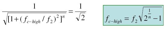
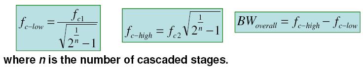
5 High cut off frequency Where n is the number of cascaded stage
6
7 2. Discuss the high frequency equivalent circuit of FET and hence derive gain bandwidth product for any one configuration. (NOV/DEC 2009). High frequency response of CS amplifier The JFET implementation of the common-source amplifier is given to the leftbelow, and the small signal circuit incorporating thehigh frequency FET model is given to the right below.as stated above, the external coupling and bypass capacitors arelarge enough that we can model them as short circuits for high frequencies.we may simplifythe small signal circuit by making the following approximations and observations:
8 ¾ rdsis usually larger than RD RL, so that the parallel combination is dominated by RD RLandrds may be neglected. If this is not the case, asingle equivalent resistance, rds RD RLmay be defined.¾ TheMillereffect transforms Cgdinto separate capacitances seen in the input and output circuits as The parallel capacitances in the input circuit, Cgsand CM1, may becombined to a single equivalent capacitance of value Similarly, the parallel capacitances in the output circuit, Cdsand CM2, may be combined to a single equivalent capacitance of value With theabove simplifications, the small signal circuit may be Cin:SettingCpitand CS equalto zero (open circuit),the equivalentresistanceseen by Cinis Cout:Letting the impedance of Cin be equalto infinity, the equivalent resistanceseen by Coutis
9 The highfrequency time constants for the CS amplifier are therefore defined the upper corner frequency is approximated by Highequency cutoff is given bygenerally, 3. Discuss the low frequency response and the high frequency response of an amplifier. (16) (APR/MAY 2010)
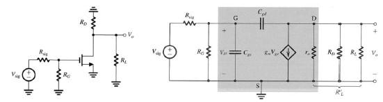
10 4. Explain the operation of high frequency common source FET amplifier with neat diagram. Derive the expression for (i) voltage gain (ii) input admittance (iii) input capacitance (iv) output admittance. (16) (APR/MAY 2010)
11
12 5. Draw the Hybrid π? equivalent circuit of a BJT. (4) (ii) Using hybrid? model, draw the high frequency equivalent circuit of CE amplifier and derive for higher cut-off frequencies. (12) (NOV/DEC 2010) Common Emitter Amplifier DC analysis: Recall that an emitter resistor is necessary to provide stability of the bias point. As such, the circuit conguration as is shown has as a poor bias. We need to include RE for good biasing (DC signals) and eliminate it for AC signals.the solution to include an emitter resistance and use a \bypass" capacitor to shortit out for AC signals as is shown. AC analysis: To start the analysis, we kill all DC sources, combine R1 and R2 into RB and replace the BJT with its small signal model. We see that emitter is now common between input and output AC signals (thus, common emitter amplifier. Analysis of this circuit is straightforward. Examination of the circuit shows that:
13
14
15 6. Explain in detail with neat diagram frequency response of BJT amplifier. Discuss the significance of cut off frequencies and Bandwidth of the amplifier. (16) (NOV/DEC 2011)
16 7. Derive the expression for frequency response of multistage amplifier. (10)(ii) discuss the significance of cut off frequencies and Gain bandwidth product of amplifier. (6) (NOV/DEC 2011) (NOV/DEC 12) The gain bandwidth product (designated as GBWP, GBW, GBP or GB) for an amplifier is the product of the amplifier'sbandwidth and the gain at which the bandwidth is measured.
17
18
19 8. Define fα,fβ and ft and state the relation between fβ and ft Alpha cutoff frequency, falpha is the frequency at which the α falls to of low frequency α,0 α=0.707α0. Alpha cutoff and beta cutoff are nearly equal: falpha ft Beta cutoff ft is the preferred figure of merit of high frequency performance. fmax is the highest frequency of oscillation possible under the most favorable conditions of bias and impedance matching. It is the frequency at which the power gain is unity. All of the output is fed back to the input to sustain oscillations. fmax is an upper limit for frequency of operation of a transistor as an active device. Though, a practical amplifier would not be usable at fmax. Beta cutoff frequency fβ is the frequency at which ω = ωβ i.e. the magnitude of the common-emitter current gain decreases by a factor of 2
20 Common emitter cutoff frequency fτ is the frequency at which the magnitude of the common emitter current gain equals unity, that is, βω = Define unity gain frequency. Obtain the necessary relation using transistor frequency response. It is a frequency at which the short circuit current gain f the CE amplifier is unity. The gain ratio for CE amplifier is A i = h fe / At f=f T A i = 1 (f T / f β ) 2 >>1 1= h fe/ (f T / f β ) (f T / f β )= h fe f T = h fe f β A(f) = 1 = gm/ 2πCcf Fu = gm/ 2πCc A i = - h fe / 1+j h fe (f/f T )
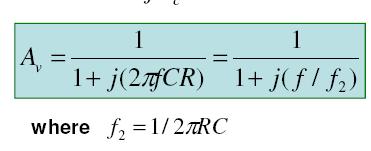
21 10. Discuss the frequency response characteristics of RC coupled amplifier. (NOV/DEC 12) frequency response curve of a RC coupled amplifier. The curve is usually plotted on a semilog graph paper with frequency range on logarithmic scale so that large frequency range can be accommodated. The gain is constant for a limited band of frequencies. This range is called mid-frequency band and gain is called mid band gain. A VM. On both sides of the mid frequency range, the gain decreases. For very low and very high frequencies the gain is almost zero. In mid band frequency range, the coupling capacitors and bypass capacitors are as good as short circuits. But when the frequency is low. These capacitors can no longer be replaced by the short circuit approximation. First consider coupling capacitor. The ac equivalent is shown in fig. 3, assuming capacitors are offering some impedance. In mid-frequency band, the capacitors are ac shorted so the input voltage appears directly across br' e but at low frequency the X C is significant and some voltage drops across X C. The input v in at the base decreases. Thus decreasing output voltage. The lower the frequency the more will be X C and lesser will be the output voltage.
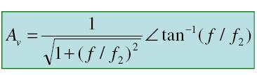
22 Fig. 3 Similarly at low frequency, output capacitor reactance also increases. The voltage across R L also reduces because some voltage drop takes place across X C. Thus output voltage reduces.the X C reactance not only reduces the gain but also change the phase between input and output. It would not be exactly 180 o but decided by the reactance. At zero frequency, the capacitors are open circuited therefore output voltage reduces to zero. The other component due to which gain decreases at low frequencies is the bypass capacitor. The function of this capacitor is to bypass ac and blocks Thus the effective voltage input is reduced. The output also reduces. The lower the frequency, the lesser will be the gain. This reduction in gain is due The capacitor C bc between the base and the collector connects the output with the input. Because of this, negative Bandwidth of an amplifier: The gain is constant over a frequency range. The frequencies at which the gain reduces to 70.7% of the maximum gain are known as cut off frequencies, upper cut off and lower cut off frequency. fig. shows these two frequencies. The difference of these two frequencies is called Band width (BW) of an amplifier. BW = f 2 f 1. Fig. 7
23 At f 1 and f 2, the voltage gain becomes Am(1 / Ö 2). The output voltage reduces to 1 / Ö 2 of maximum output voltage. Since the power is proportional to voltage square, the output power at these frequencies becomes half of maximum power. The gain on db scale is given by 20 log10(v2 / V1) = 10 log 10 (V2 / V1)2 = 3 db. 20 log10(v2 / V1) = 20 log10(0.707) =10 log10 (1 / Ö 2)2 = 10 log10(1 / 2) = -3 db. If the difference in gain is more than 3 db, then it can be detected by human. If it is less than 3 db it cannot be detected.
UNIT I BIASING OF DISCRETE BJT AND MOSFET PART A
 UNIT I BIASING OF DISCRETE BJT AND MOSFET PART A 1. Why do we choose Q point at the center of the load line? 2. Name the two techniques used in the stability of the q point.explain. 3. Give the expression
ESE319 Introduction to Microelectronics High Frequency BJT Model & Cascode BJT Amplifier
 High Frequency BJT Model & Cascode BJT Amplifier 1 Gain of 10 Amplifier Non-ideal Transistor C in R 1 V CC R 2 v s Gain starts dropping at > 1MHz. Why! Because of internal transistor capacitances that
Lecture #7 BJT and JFET Frequency Response
 November 2014 Integrated Technical Education Cluster At AlAmeeria J-601-1448 Electronic Principals Lecture #7 BJT and JFET Frequency Response Instructor: Dr. Ahmad El-Banna Agenda Introduction General
SIDDHARTH GROUP OF INSTITUTIONS :: PUTTUR (AUTONOMOUS) Siddharth Nagar, Narayanavanam Road QUESTION BANK
 Siddharth Nagar, Narayanavanam Road QUESTION BANK") SIDDHARTH GROUP OF INSTITUTIONS :: PUTTUR (AUTONOMOUS) Siddharth Nagar, Narayanavanam Road 517583 QUESTION BANK Subject with Code : Electronic Circuit Analysis (16EC407) Year & Sem: II-B.Tech & II-Sem
SIDDHARTH GROUP OF INSTITUTIONS :: PUTTUR (AUTONOMOUS) Siddharth Nagar, Narayanavanam Road 517583 QUESTION BANK Subject with Code : Electronic Circuit Analysis (16EC407) Year & Sem: II-B.Tech & II-Sem
BJT Circuits (MCQs of Moderate Complexity)
") BJT Circuits (MCQs of Moderate Complexity) 1. The current ib through base of a silicon npn transistor is 1+0.1 cos (1000πt) ma. At 300K, the rπ in the small signal model of the transistor is i b B C r
BJT Circuits (MCQs of Moderate Complexity) 1. The current ib through base of a silicon npn transistor is 1+0.1 cos (1000πt) ma. At 300K, the rπ in the small signal model of the transistor is i b B C r
ECE 255, Discrete-Circuit Amplifiers
 ECE 255, Discrete-Circuit Amplifiers 20 March 2018 In this lecture, we will continue with the study of transistor amplifiers with the presence of biasing circuits and coupling capacitors in place. We will
ESE 372 / Spring 2011 / Lecture 19 Common Base Biased by current source
 ESE 372 / Spring 2011 / Lecture 19 Common Base Biased by current source Output from Collector Start with bias DC analysis make sure BJT is in FA, then calculate small signal parameters for AC analysis.
 Pg: 1 VALLIAMMAI ENGINEERING COLLEGE SRM Nagar, Kattankulathur 603 203 Department of Electronics & Communication Engineering Regulation: 2013 Acadamic Year : 2015 2016 EC6304 Electronic Circuits I Question
Improving Amplifier Voltage Gain
 15.1 Multistage ac-coupled Amplifiers 1077 TABLE 15.3 Three-Stage Amplifier Summary HAND ANALYSIS SPICE RESULTS Voltage gain 998 1010 Input signal range 92.7 V Input resistance 1 M 1M Output resistance
G.PULLAIAH COLLEGE OF ENGINEERING & TECHNOLOGY II B.Tech II-SEM MID -I EXAM Branch: EEE Sub: Analog Electronic Circuits Date:
 G.PULLAIAH COLLEGE OF ENGINEERING & TECHNOLOGY II B.Tech II-SEM MID -I EXAM Branch: EEE Sub: Analog Electronic Circuits Date: 08-03-18 Time: 20 minutes Max.Marks:10 1. The amplifier that gives unity current
PartIIILectures. Multistage Amplifiers
 University of missan Electronic II, Second year 2015-2016 PartIIILectures Assistant Lecture: 1 Multistage and Compound Amplifiers Basic Definitions: 1- Gain of Multistage Amplifier: Fig.(1-1) A general
Electronics Prof. D. C. Dube Department of Physics Indian Institute of Technology, Delhi
 Electronics Prof. D. C. Dube Department of Physics Indian Institute of Technology, Delhi Module No # 05 FETS and MOSFETS Lecture No # 06 FET/MOSFET Amplifiers and their Analysis In the previous lecture
ELC224 Final Review (12/10/2009) Name:
 Name:") ELC224 Final Review (12/10/2009) Name: Select the correct answer to the problems 1 through 20. 1. A common-emitter amplifier that uses direct coupling is an example of a dc amplifier. 2. The frequency
ELC224 Final Review (12/10/2009) Name: Select the correct answer to the problems 1 through 20. 1. A common-emitter amplifier that uses direct coupling is an example of a dc amplifier. 2. The frequency
Last time: BJT CE and CB amplifiers biased by current source
 Last time: BJT CE and CB amplifiers biased by current source Assume FA regime, then VB VC V E I B I E, β 1 I Q C α I, V 0. 7V Calculate V CE and confirm it is > 0.2-0.3V, then BJT can be replaced with
UNIVERSITY PART-B ANSWERS UNIT-1
 UNERSTY PART-B ANSWERS UNT-. Discuss about the DC load line and Q point. (OR) What is D.C. load line, how will you select the operating point, explain it using common emitter amplifier characteristics
Unit- I- Biasing Of Discrete BJT and MOSFET
 Part- A QUESTIONS: Unit- I- Biasing Of Discrete BJT and MOSFET 1. Describe about BJT? BJT consists of 2 PN junctions. It has three terminals: emitter, base and collector. Transistor can be operated in
5.25Chapter V Problem Set
 5.25Chapter V Problem Set P5.1 Analyze the circuits in Fig. P5.1 and determine the base, collector, and emitter currents of the BJTs as well as the voltages at the base, collector, and emitter terminals.
Document Name: Electronic Circuits Lab. Facebook: Twitter:
 Document Name: Electronic Circuits Lab www.vidyathiplus.in Facebook: www.facebook.com/vidyarthiplus Twitter: www.twitter.com/vidyarthiplus Copyright 2011-2015 Vidyarthiplus.in (VP Group) Page 1 CIRCUIT
II/IV B. TECH. DEGREE EXAMINATIONS, NOVEMBER Second Semester EC/EE ELECTRONIC CIRCUIT ANALYSIS. Time : Three Hours Max.
 Total No. of Questions : 9] [Total No. of Pages : 02 B.Tech. II/ IV YEAR DEGREE EXAMINATION, APRIL/MAY - 2014 (Second Semester) EC/EE/EI Electronic Circuit Analysis Time : 03 Hours Maximum Marks : 70 Q1)
Basic electronics Prof. T.S. Natarajan Department of Physics Indian Institute of Technology, Madras Lecture- 17. Frequency Analysis
 Basic electronics Prof. T.S. Natarajan Department of Physics Indian Institute of Technology, Madras Lecture- 17 Frequency Analysis Hello everybody! In our series of lectures on basic electronics learning
INSTITUTE OF AERONAUTICAL ENGINEERING (AUTONOMUS) Dundigal, Hyderabad
 Dundigal, Hyderabad") INSTITUTE OF AERONAUTICAL ENGINEERING (AUTONOMUS) Dundigal, Hyderabad - 00 0 ELECTRONICS AND COMMUNICATION ENGINEERING ASSIGNMENT Name : ELECTRONIC CIRCUIT ANALYSIS Code : A0 Class : II - B. Tech nd semester
INSTITUTE OF AERONAUTICAL ENGINEERING (AUTONOMUS) Dundigal, Hyderabad - 00 0 ELECTRONICS AND COMMUNICATION ENGINEERING ASSIGNMENT Name : ELECTRONIC CIRCUIT ANALYSIS Code : A0 Class : II - B. Tech nd semester
EC1203: ELECTRONICS CIRCUITS-I UNIT-I TRANSISTOR BIASING PART-A
 SHRI ANGALAMMAN COLLEGE OF ENGG & TECH., TRICHY 621105 (Approved by AICTE, New Delhi and Affiliated to Anna University Chennai/Trichy) ( ISO 9001:2008 Certified Institution) DEPARTMENT OF ELECTRONICS &
EXPERIMENT 1: LOW AND HIGH FREQUENCY REGION ANALYSIS OF BJT AMPLIFIERS
 EXPERIMENT 1: LOW AND HIGH FREQUENCY REGION ANALYSIS OF BJT AMPLIFIERS Objective: In single layer common emitter amplifiers, observation of frequency dependence. Materials Transistor: 1x BC237 transistor
BJT & FET Frequency Response
 Chapter 4 BJT & FET Spring 2012 4 th Semester Mechatronics SZABIST, Karachi 2 Course Support humera.rafique@szabist.edu.pk Office: 100 Campus (404) Official: ZABdesk Subsidiary: https://sites.google.com/site/zabistmechatronics/home/spring-2012/ecd
Tutorial 2 BJTs, Transistor Bias Circuits, BJT Amplifiers FETs and FETs Amplifiers. Part 1: BJTs, Transistor Bias Circuits and BJT Amplifiers
 Tutorial 2 BJTs, Transistor Bias Circuits, BJT Amplifiers FETs and FETs Amplifiers Part 1: BJTs, Transistor Bias Circuits and BJT Amplifiers 1. Explain the purpose of a thin, lightly doped base region.
Midterm 2 Exam. Max: 90 Points
 Midterm 2 Exam Name: Max: 90 Points Question 1 Consider the circuit below. The duty cycle and frequency of the 555 astable is 55% and 5 khz respectively. (a) Determine a value for so that the average current
UNIT I PN JUNCTION DEVICES
 UNIT I PN JUNCTION DEVICES 1. Define Semiconductor. 2. Classify Semiconductors. 3. Define Hole Current. 4. Define Knee voltage of a Diode. 5. What is Peak Inverse Voltage? 6. Define Depletion Region in
 VALLIAMMAI ENGINEERING COLLEGE SRM NAGAR, KATTANKULATHUR- 603 203 DEPARTMENT OF ELECTRONICS AND COMMUNICATION ENGINEERING EC6202- ELECTRONIC DEVICES AND CIRCUITS UNIT I PN JUNCTION DEVICES 1. Define Semiconductor.
 UNIVERSITY PART-A ANSWERS Unit-1 1. What is an amplifier? An amplifier is a device which produces a large electrical output of similar characteristics to that of the input parameters. 2. What are transistors?
 Code No: Y0221/R07 Set No. 1 I B.Tech Supplementary Examinations, Apr/May 2013 BASIC ELECTRONIC DEVICES AND CIRCUITS (Electrical & Electronics Engineering) Time: 3 hours Max Marks: 80 Answer any FIVE Questions
Code: 9A Answer any FIVE questions All questions carry equal marks *****
 II B. Tech II Semester (R09) Regular & Supplementary Examinations, April/May 2012 ELECTRONIC CIRCUIT ANALYSIS (Common to EIE, E. Con. E & ECE) Time: 3 hours Max Marks: 70 Answer any FIVE questions All
Electronics Lab. (EE21338)
") Princess Sumaya University for Technology The King Abdullah II School for Engineering Electrical Engineering Department Electronics Lab. (EE21338) Prepared By: Eng. Eyad Al-Kouz October, 2012 Table of
Princess Sumaya University for Technology The King Abdullah II School for Engineering Electrical Engineering Department Electronics Lab. (EE21338) Prepared By: Eng. Eyad Al-Kouz October, 2012 Table of
FREQUENTLY ASKED QUESTIONS
 FREQUENTLY ASKED QUESTIONS UNIT-1 SUBJECT : ELECTRONIC DEVICES AND CIRCUITS SUBJECT CODE : EC6202 BRANCH: EEE PART -A 1. What is meant by diffusion current in a semi conductor? (APR/MAY 2010, 2011, NOV/DEC
EXPT NO: 1.A. COMMON EMITTER AMPLIFIER (Software) PRELAB:
 PRELAB:") EXPT NO: 1.A COMMON EMITTER AMPLIFIER (Software) PRELAB: 1. Study the operation and working principle of CE amplifier. 2. Identify all the formulae you will need in this Lab. 3. Study the procedure of
EXPT NO: 1.A COMMON EMITTER AMPLIFIER (Software) PRELAB: 1. Study the operation and working principle of CE amplifier. 2. Identify all the formulae you will need in this Lab. 3. Study the procedure of
Chapter.8: Oscillators
 Chapter.8: Oscillators Objectives: To understand The basic operation of an Oscillator the working of low frequency oscillators RC phase shift oscillator Wien bridge Oscillator the working of tuned oscillator
Skyup's Media ELECTRONIC CIRCUIT ANALYSIS
 ELECTRONIC CIRCUIT ANALYSIS MALLAREDDY COLLEGE OF ENGINEERING AND TECHNOLOGY DEPARTMENT OF ELECTROINICS AND COMMUNICATION ENGINEERING Answer all the following questions: PART A: B.TECH II YEAR II SEMESTER
Chapter 15 Goals. ac-coupled Amplifiers Example of a Three-Stage Amplifier
 Chapter 15 Goals ac-coupled multistage amplifiers including voltage gain, input and output resistances, and small-signal limitations. dc-coupled multistage amplifiers. Darlington configuration and cascode
BASIC ELECTRONICS PROF. T.S. NATARAJAN DEPT OF PHYSICS IIT MADRAS
 BASIC ELECTRONICS PROF. T.S. NATARAJAN DEPT OF PHYSICS IIT MADRAS LECTURE-13 Basic Characteristic of an Amplifier Simple Transistor Model, Common Emitter Amplifier Hello everybody! Today in our series
Lecture #3 ( 2 weeks) Transistors
 Transistors") Spring 2015 Benha University Faculty of Engineering at Shoubra ECE-291 Electronic Engineering Lecture #3 ( 2 weeks) Transistors Instructor: Dr. Ahmad El-Banna 1 Agenda BJT Structure Basic Operation Transistor
Spring 2015 Benha University Faculty of Engineering at Shoubra ECE-291 Electronic Engineering Lecture #3 ( 2 weeks) Transistors Instructor: Dr. Ahmad El-Banna 1 Agenda BJT Structure Basic Operation Transistor
Transistors and Applications
 Chapter 17 Transistors and Applications DC Operation of Bipolar Junction Transistors (BJTs) The bipolar junction transistor (BJT) is constructed with three doped semiconductor regions separated by two
Code No: R Set No. 1
 Code No: R059210404 Set No. 1 II B.Tech I Semester Supplimentary Examinations, February 2008 ELECTRONIC CIRCUIT ANALYSIS ( Common to Electronics & Communication Engineering and Electronics & Telematics)
(b) 25% (b) increases
 25% (b) increases") Homework Assignment 07 Question 1 (2 points each unless noted otherwise) 1. In the circuit 10 V, 10, and 5K. What current flows through? Answer: By op-amp action the voltage across is and the current through
Homework Assignment 07 Question 1 (2 points each unless noted otherwise) 1. In the circuit 10 V, 10, and 5K. What current flows through? Answer: By op-amp action the voltage across is and the current through
UNIT 1 MULTI STAGE AMPLIFIES
 UNIT 1 MULTI STAGE AMPLIFIES 1. a) Derive the equation for the overall voltage gain of a multistage amplifier in terms of the individual voltage gains. b) what are the multi-stage amplifiers? 2. Describe
EEE225: Analogue and Digital Electronics
 EEE225: Analogue and Digital Electronics Lecture II James E. Green Department of Electronic Engineering University of Sheffield j.e.green@sheffield.ac.uk This Lecture 1 One Transistor Circuits Continued...
Electronics Prof D. C. Dube Department of Physics Indian Institute of Technology, Delhi
 Electronics Prof D. C. Dube Department of Physics Indian Institute of Technology, Delhi Module No. # 04 Feedback in Amplifiers, Feedback Configurations and Multi Stage Amplifiers Lecture No. # 03 Input
Gechstudentszone.wordpress.com
 UNIT 4: Small Signal Analysis of Amplifiers 4.1 Basic FET Amplifiers In the last chapter, we described the operation of the FET, in particular the MOSFET, and analyzed and designed the dc response of circuits
Homework Assignment 12
 Homework Assignment 12 Question 1 Shown the is Bode plot of the magnitude of the gain transfer function of a constant GBP amplifier. By how much will the amplifier delay a sine wave with the following
MAHALAKSHMI ENGINEERING COLLEGE TIRUCHIRAPALLI UNIT III TUNED AMPLIFIERS PART A (2 Marks)
") MAHALAKSHMI ENGINEERING COLLEGE TIRUCHIRAPALLI-621213. UNIT III TUNED AMPLIFIERS PART A (2 Marks) 1. What is meant by tuned amplifiers? Tuned amplifiers are amplifiers that are designed to reject a certain
MAHALAKSHMI ENGINEERING COLLEGE TIRUCHIRAPALLI-621213. UNIT III TUNED AMPLIFIERS PART A (2 Marks) 1. What is meant by tuned amplifiers? Tuned amplifiers are amplifiers that are designed to reject a certain
Homework Assignment 11
 Homework Assignment 11 Question 1 (Short Takes) Two points each unless otherwise indicated. 1. What is the 3-dB bandwidth of the amplifier shown below if r π = 2.5K, r o = 100K, g m = 40 ms, and C L =
BJT. Bipolar Junction Transistor BJT BJT 11/6/2018. Dr. Satish Chandra, Assistant Professor, P P N College, Kanpur 1
 BJT Bipolar Junction Transistor Satish Chandra Assistant Professor Department of Physics P P N College, Kanpur www.satish0402.weebly.com The Bipolar Junction Transistor is a semiconductor device which
UNIVERSITY OF NORTH CAROLINA AT CHARLOTTE Department of Electrical and Computer Engineering
 UNIVERSITY OF NORTH CAROLINA AT CHARLOTTE Department of Electrical and Computer Engineering EXPERIMENT 7 BJT AMPLIFIER CONFIGURATIONS AND INPUT/OUTPUT IMPEDANCE OBJECTIVES The purpose of this experiment
The George Washington University School of Engineering and Applied Science Department of Electrical and Computer Engineering ECE 20 - LAB
 The George Washington University School of Engineering and Applied Science Department of Electrical and Computer Engineering ECE 20 - LAB Experiment # 6 (Part I) Bipolar Junction Transistors Common Emitter
SUMMER 13 EXAMINATION Subject Code: Model Answer Page No: / N
 Important Instructions to examiners: 1) The answers should be examined by key words and not as word-to-word as given in the model answer scheme. 2) The model answer and the answer written by candidate
Frequency Response of Common Emitter Amplifier
 Başkent University Department of Electrical and Electronics Engineering EEM 311 Electronics II Experiment 6 Frequency Response of Common Emitter Amplifier Aim: The aim of this experiment is to study the
Small signal ac equivalent circuit of BJT
 UNIT-2 Part A 1. What is an ac load line? [N/D 16] A dc load line gives the relationship between the q-point and the transistor characteristics. When capacitors are included in a CE transistor circuit,
In a cascade configuration, the overall voltage and current gains are given by:
 ECE 3274 Two-Stage Amplifier Project 1. Objective The objective of this lab is to design and build a direct coupled two-stage amplifier, including a common-source gain stage and a common-collector buffer
TUNED AMPLIFIERS 5.1 Introduction: Coil Losses:
 TUNED AMPLIFIERS 5.1 Introduction: To amplify the selective range of frequencies, the resistive load R C is replaced by a tuned circuit. The tuned circuit is capable of amplifying a signal over a narrow
Operational Amplifier BME 360 Lecture Notes Ying Sun
 Operational Amplifier BME 360 Lecture Notes Ying Sun Characteristics of Op-Amp An operational amplifier (op-amp) is an analog integrated circuit that consists of several stages of transistor amplification
ECE 3274 Common-Emitter Amplifier Project
 ECE 3274 Common-Emitter Amplifier Project 1. Objective The objective of this lab is to design and build the common-emitter amplifier with partial bypass of the emitter resistor to control the AC voltage
Amplifier Frequency Response, Feedback, Oscillations; Op-Amp Block Diagram and Gain-Bandwidth Product
 Amplifier Frequency Response, Feedback, Oscillations; Op-Amp Block Diagram and Gain-Bandwidth Product Physics116A,12/4/06 Draft Rev. 1, 12/12/06 D. Pellett 2 Negative Feedback and Voltage Amplifier AB
2. SINGLE STAGE BIPOLAR JUNCTION TRANSISTOR (BJT) AMPLIFIERS
 AMPLIFIERS") 2. SINGLE STAGE BIPOLAR JUNCTION TRANSISTOR (BJT) AMPLIFIERS I. Objectives and Contents The goal of this experiment is to become familiar with BJT as an amplifier and to evaluate the basic configurations
2. SINGLE STAGE BIPOLAR JUNCTION TRANSISTOR (BJT) AMPLIFIERS I. Objectives and Contents The goal of this experiment is to become familiar with BJT as an amplifier and to evaluate the basic configurations
SAMPLE FINAL EXAMINATION FALL TERM
 ENGINEERING SCIENCES 154 ELECTRONIC DEVICES AND CIRCUITS SAMPLE FINAL EXAMINATION FALL TERM 2001-2002 NAME Some Possible Solutions a. Please answer all of the questions in the spaces provided. If you need
ECE 3274 Common-Collector (Emitter-Follower) Amplifier Project
 Amplifier Project") ECE 3274 Common-Collector (Emitter-Follower) Amplifier Project 1. Objective This project will show the biasing, gain, frequency response, and impedance properties of a common collector amplifier. 2. Components
ECE 3274 Common-Collector (Emitter-Follower) Amplifier Project 1. Objective This project will show the biasing, gain, frequency response, and impedance properties of a common collector amplifier. 2. Components
Homework Assignment 06
 Homework Assignment 06 Question 1 (Short Takes) One point each unless otherwise indicated. 1. Consider the current mirror below, and neglect base currents. What is? Answer: 2. In the current mirrors below,
Vel Tech High Tech Dr.Ranagarajan Dr.Sakunthala Engineering College Department of ECE
 Course Code: EC8351 Course Name: ELECTRONIC CIRCUITS I L-3 : T-0 : P-0 : Credits - 3 COURSE OBJECTIVES: To understand the methods of biasing transistors To design and analyze single stage and multistage
(a) BJT-OPERATING MODES & CONFIGURATIONS
 BJT-OPERATING MODES & CONFIGURATIONS") (a) BJT-OPERATING MODES & CONFIGURATIONS 1. The leakage current I CBO flows in (a) The emitter, base and collector leads (b) The emitter and base leads. (c) The emitter and collector leads. (d) The base
(a) BJT-OPERATING MODES & CONFIGURATIONS 1. The leakage current I CBO flows in (a) The emitter, base and collector leads (b) The emitter and base leads. (c) The emitter and collector leads. (d) The base
By: Dr. Ahmed ElShafee
 Lecture (04) Transistor Bias Circuit 3 BJT Amplifiers 1 By: Dr. Ahmed ElShafee ١ Emitter Feedback Bias If an emitter resistor is added to the base bias circuit in Figure, the result is emitter feedback
GOVERNMENT OF KARNATAKA KARNATAKA STATE PRE-UNIVERSITY EDUCATION EXAMINATION BOARD II YEAR PUC EXAMINATION JULY-2012 SCHEME OF VALUATION
 GOVERNMENT OF KARNATAKA KARNATAKA STATE PRE-UNIVERSITY EDUCATION EXAMINATION BOARD II YEAR PUC EXAMINATION JULY-0 SCHEME OF VALUATION Subject Code: 40 Subject: PART - A 0. Which region of the transistor
Mini Project 3 Multi-Transistor Amplifiers. ELEC 301 University of British Columbia
 Mini Project 3 Multi-Transistor Amplifiers ELEC 30 University of British Columbia 4463854 November 0, 207 Contents 0 Introduction Part : Cascode Amplifier. A - DC Operating Point.......................................
Experiment No. 9 DESIGN AND CHARACTERISTICS OF COMMON BASE AND COMMON COLLECTOR AMPLIFIERS
 Experiment No. 9 DESIGN AND CHARACTERISTICS OF COMMON BASE AND COMMON COLLECTOR AMPLIFIERS 1. Objective: The objective of this experiment is to explore the basic applications of the bipolar junction transistor
ECE 255, MOSFET Amplifiers
 ECE 255, MOSFET Amplifiers 26 October 2017 In this lecture, the basic configurations of MOSFET amplifiers will be studied similar to that of BJT. Previously, it has been shown that with the transistor
ECE 3274 Common-Emitter Amplifier Project
 ECE 3274 Common-Emitter Amplifier Project 1. Objective The objective of this lab is to design and build three variations of the common- emitter amplifier. 2. Components Qty Device 1 2N2222 BJT Transistor
Electronic Troubleshooting. Chapter 5 Multistage Amplifiers
 Electronic Troubleshooting Chapter 5 Multistage Amplifiers Overview When more amplification is required than can be supplied by a single stage amp A second stage is added Or more stages are added Aspects
Transistor Biasing. DC Biasing of BJT. Transistor Biasing. Transistor Biasing 11/23/2018
 Transistor Biasing DC Biasing of BJT Satish Chandra Assistant Professor Department of Physics P P N College, Kanpur www.satish0402.weebly.com A transistors steady state of operation depends a great deal
Homework Assignment 05
 Homework Assignment 05 Question (2 points each unless otherwise indicated)(20 points). Estimate the parallel parasitic capacitance of a mh inductor with an SRF of 220 khz. Answer: (2π)(220 0 3 ) = ( 0
Code No: R Set No. 1
 Code No: R05010204 Set No. 1 I B.Tech Supplimentary Examinations, Aug/Sep 2007 ELECTRONIC DEVICES AND CIRCUITS ( Common to Electrical & Electronic Engineering, Electronics & Communication Engineering,
Chapter 6. BJT Amplifiers
 Basic Electronic Devices and Circuits EE 111 Electrical Engineering Majmaah University 2 nd Semester 1432/1433 H Chapter 6 BJT Amplifiers 1 Introduction The things you learned about biasing a transistor
Phy 335, Unit 4 Transistors and transistor circuits (part one)
") Mini-lecture topics (multiple lectures): Phy 335, Unit 4 Transistors and transistor circuits (part one) p-n junctions re-visited How does a bipolar transistor works; analogy with a valve Basic circuit
Mini-lecture topics (multiple lectures): Phy 335, Unit 4 Transistors and transistor circuits (part one) p-n junctions re-visited How does a bipolar transistor works; analogy with a valve Basic circuit
Page 1 of 7. Power_AmpFal17 11/7/ :14
 ECE 3274 Power Amplifier Project (Push Pull) Richard Cooper 1. Objective This project will introduce two common power amplifier topologies, and also illustrate the difference between a Class-B and a Class-AB
Page 1. Telecommunication Electronics ETLCE - A2 06/09/ DDC 1. Politecnico di Torino ICT School. Amplifiers
 Politecnico di Torino ICT School Amplifiers Telecommunication Electronics A2 Transistor amplifiers» Bias point and circuits,» Small signal models» Gain and bandwidth» Limits of linear analysis Op Amp amplifiers
Lab 4 : Transistor Oscillators
 Objective: Lab 4 : Transistor Oscillators In this lab, you will learn how to design and implement a colpitts oscillator. In part II you will implement a RC phase shift oscillator Hardware Required : Pre
Differential Amplifier Design
 Differential Amplifier Design Design with ideal current source bias. Differential and common mode gain results Add finite output resistance to current source. Replace ideal current source with current
UNIT I. Small Signal High Frequency Transistor Amplifier models
 UNIT I Small Signal High Frequency Transistor Amplifier models BJT: Transistor at high frequencies, Hybrid- π common emitter transistor model, Hybrid π conductances, Hybrid π capacitances, validity of
EE LINEAR INTEGRATED CIRCUITS & APPLICATIONS
 UNITII CHARACTERISTICS OF OPAMP 1. What is an opamp? List its functions. The opamp is a multi terminal device, which internally is quite complex. It is a direct coupled high gain amplifier consisting of
Lecture (06) BJT Amplifiers 3
 BJT Amplifiers 3") Lecture (06) BJT Amplifiers 3 By: Dr. Ahmed ElShafee 1 Current Gain 2 Power Gain The overall power gain is the product of the overall voltage gain (Av ) and the overall current gain (Ai). 3 THE COMMON
Lecture (06) BJT Amplifiers 3 By: Dr. Ahmed ElShafee 1 Current Gain 2 Power Gain The overall power gain is the product of the overall voltage gain (Av ) and the overall current gain (Ai). 3 THE COMMON
ECE 2201 PRELAB 6 BJT COMMON EMITTER (CE) AMPLIFIER
 AMPLIFIER") ECE 2201 PRELAB 6 BJT COMMON EMITTER (CE) AMPLIFIER Hand Analysis P1. Determine the DC bias for the BJT Common Emitter Amplifier circuit of Figure 61 (in this lab) including the voltages V B, V C and V
ECE 2201 PRELAB 6 BJT COMMON EMITTER (CE) AMPLIFIER Hand Analysis P1. Determine the DC bias for the BJT Common Emitter Amplifier circuit of Figure 61 (in this lab) including the voltages V B, V C and V
55:041 Electronic Circuits The University of Iowa Fall Exam 3. Question 1 Unless stated otherwise, each question below is 1 point.
 Exam 3 Name: Score /65 Question 1 Unless stated otherwise, each question below is 1 point. 1. An engineer designs a class-ab amplifier to deliver 2 W (sinusoidal) signal power to an resistive load. Ignoring
ET215 Devices I Unit 4A
 ITT Technical Institute ET215 Devices I Unit 4A Chapter 3, Section 3.1-3.2 This unit is divided into two parts; Unit 4A and Unit 4B Chapter 3 Section 3.1 Structure of Bipolar Junction Transistors The basic
ELECTRONIC CIRCUIT ANALYSIS LECTURE NOTES B.TECH (II YEAR II SEM) ( )
 ( )") ELECTRONIC CIRCUIT ANALYSIS LECTURE NOTES B.TECH (II YEAR II SEM) (2017-18) Prepared by: Mr. V. Shiva Rajkumar, Assistant Professor Mr. E. Mahendar Reddy, Assistant Professor Department of Electronics
ELECTRONIC CIRCUIT ANALYSIS LECTURE NOTES B.TECH (II YEAR II SEM) (2017-18) Prepared by: Mr. V. Shiva Rajkumar, Assistant Professor Mr. E. Mahendar Reddy, Assistant Professor Department of Electronics
Oscillators. An oscillator may be described as a source of alternating voltage. It is different than amplifier.
 Oscillators An oscillator may be described as a source of alternating voltage. It is different than amplifier. An amplifier delivers an output signal whose waveform corresponds to the input signal but
SKP Engineering College
 SKP Engineering College Tiruvannamalai 606611 A Course Material on Electronic Circuits I By M.Jerin Jose Assistant Professor Electronics and Communication Engineering Department Electronics and Communication
Electrical, Electronic and Digital Principles (EEDP) Lecture 5. CE Amplifier, Coupling, and Multistage Amplifiers باسم ممدوح الحلوانى
 Lecture 5. CE Amplifier, Coupling, and Multistage Amplifiers باسم ممدوح الحلوانى") Electrical, Electronic and Digital Principles (EEDP) Lecture 5 CE Amplifier, Coupling, and Multistage Amplifiers د. باسم ممدوح الحلوانى Total Output Resistance The output resistance of any system is defined
Electrical, Electronic and Digital Principles (EEDP) Lecture 5 CE Amplifier, Coupling, and Multistage Amplifiers د. باسم ممدوح الحلوانى Total Output Resistance The output resistance of any system is defined
Scheme Q.1 Attempt any SIX of following: 12-Total Marks a) Draw symbol NPN and PNP transistor. 2 M Ans: Symbol Of NPN and PNP BJT (1M each)
 Draw symbol NPN and PNP transistor. 2 M Ans: Symbol Of NPN and PNP BJT (1M each)") Q. No. WINTER 16 EXAMINATION (Subject Code: 17319) Model Answer Important Instructions to examiners: 1) The answers should be examined by key words and not as word-to-word as given in the model answer
Q. No. WINTER 16 EXAMINATION (Subject Code: 17319) Model Answer Important Instructions to examiners: 1) The answers should be examined by key words and not as word-to-word as given in the model answer
DHANALAKSHMI COLLEGE OF ENGINEERING DEPARTMENT OF ELECTRICAL AND ELECTRONICS ENGINEERING EC6202 ELECTRONIC DEVICES AND CIRCUITS
 DHANALAKSHMI COLLEGE OF ENGINEERING DEPARTMENT OF ELECTRICAL AND ELECTRONICS ENGINEERING EC6202 ELECTRONIC DEVICES AND CIRCUITS UNIT-I - PN DIODEAND ITSAPPLICATIONS 1. What is depletion region in PN junction?
Linear electronic. Lecture No. 1
 1 Lecture No. 1 2 3 4 5 Lecture No. 2 6 7 8 9 10 11 Lecture No. 3 12 13 14 Lecture No. 4 Example: find Frequency response analysis for the circuit shown in figure below. Where R S =4kR B1 =8kR B2 =4k R
UNIT 3: FIELD EFFECT TRANSISTORS
 FIELD EFFECT TRANSISTOR: UNIT 3: FIELD EFFECT TRANSISTORS The field effect transistor is a semiconductor device, which depends for its operation on the control of current by an electric field. There are
Chapter Two "Bipolar Transistor Circuits"
 Chapter Two "Bipolar Transistor Circuits" 1.TRANSISTOR CONSTRUCTION:- The transistor is a three-layer semiconductor device consisting of either two n- and one p-type layers of material or two p- and one
Paper-1 (Circuit Analysis) UNIT-I
 UNIT-I") Paper-1 (Circuit Analysis) UNIT-I AC Fundamentals & Kirchhoff s Current and Voltage Laws 1. Explain how a sinusoidal signal can be generated and give the significance of each term in the equation? 2. Define
Paper-1 (Circuit Analysis) UNIT-I AC Fundamentals & Kirchhoff s Current and Voltage Laws 1. Explain how a sinusoidal signal can be generated and give the significance of each term in the equation? 2. Define
Assist Lecturer: Marwa Maki. Active Filters
 Active Filters In past lecture we noticed that the main disadvantage of Passive Filters is that the amplitude of the output signals is less than that of the input signals, i.e., the gain is never greater
The Miller Approximation. CE Frequency Response. The exact analysis is worked out on pp of H&S.
 CE Frequency Response The exact analysis is worked out on pp. 639-64 of H&S. The Miller Approximation Therefore, we consider the effect of C µ on the input node only V ---------- out V s = r g π m ------------------