Improved Phase Noise Model. School of Electronics and Computer Science
|
|
|
- Theodora Harrington
- 5 years ago
- Views:
Transcription
1 Improved Phase Noise Model for Ultra Wideband VCO Li Ke Reuben Wilcock Peter Wilson School of Electronics and Computer Science University of Southampton, UK
2 Presentation outline Research motivation Improved phase noise model Simulation results Measurement results Conclusions 2
3 Research motivation Typical VCO design flow Topology and number of stages chosen from experience Starting point and simulation led improvement Topology selection Design specification Choose N stages Process parameters Im mprove Transistor sizing Simulation 3
4 Research motivation Voltage controlled oscillator design challenges Lack of detailed transistor sizing guidelines which relate high h level l specifications to W and Ls. Small signal model (Barkhausen Criteria) only holds valid for linear operation. Jitter/Phase noise performance is an important specification in VCO design. Phase noise and jitter simulations in leading simulators (e.g. SpectreRF) are extremely time consuming. Requirement for a phase noise targeted transistor sizing model. 4
5 Research motivation Previous work has considered a number of factors when modelling VCO phase noise Process parameters Power supply Topology Transistor dimensions Oscillation frequency However: No one has considered the effect of frequency tuning on phase noise. 5
6 Presentation outline Research motivation Improved phase noise model Simulation results Measurement results Conclusions 6
7 (WL)=nμ (())()Improved Phase Noise model The proposed model is based on the new dual inverter delay cell which has 10 octave tuning range.[1] Vp I 1 I 2 Mp2 Mp4 Vp Mp6 Vgp Mp1 Mp3 Mp5 V in + V out + I 3 V out - Mn1 Mn3 Mn5 Vgn Vn Mn2 Vn Mn4 Mn6 Vp Vn V in - Vgp Vgp Vgp Vgp V in + V out - V in + V out - V in + V out - V in + V out - V in - V out + V in - V out + V in - V out + V in - V out + Vgn Vgn Vgn Vgn V out - V out + Previous design guidelines for this cell simply ensure that I 1 + I 2 = I 3 pμ 2V D- V tp 2WW + VD LL- V tn 2 n[1] Li Ke, Reuben Wilcock, Peter Wilson Improved 6.7GHz CMOS VCO Delay Cell With Up To Seven Octave Tuning Range, Proceddings of IEEE ISCAS, May
8 ()Improved Phase Noise model For a phase noise orientated design approach, existing models can be expressed as[2] : 2 Takes account of: Lf1KKffnfp = 2NV2CWL+ WLefox 1n1np5p5 Oscillation frequency: f 0 Process parameter: K fn,k fp, C ox Transistor dimensions: W n1,l n1, W p5, L p5 Topology: N (Generally accepted that 1/f noise dominates the spectrum up to a few MHz) 0f 3[2] Sohrab Samadian, Michael M. Green, Phase Noise in Dual Inverter-Based CMOS Ring Oscillator, Proceddings of IEEE ISCAS, May
9 ()Improved Phase Noise model What happens when the tuning voltage changes? 2Lf1fnfp 0 = 2NV2CWL+ WL f 3efox 11np5p5 n KfKDecrease V n Increase V p Decrease in Frequency (f o ) Lower gate overdrive voltage (Veff) ) Phase Noise Phase Increase Noise or Decrease? 9
10 Improved Phase Noise model Post layout simulation results (SpectreRF-PSS-Pnoise) Example 1(W/L)um Example 2(W/L)um Mn1,Mn2 40/0.13 Mn1,Mn2 64/0.4 Mp5,Mp6 103/0.13 Mp5,Mp6 202/0.4 Mn3 Mn6 20/0.13 Mn3 Mn6 32/0.4 Mp1 Mp4 51.5/0.13 Mp1 Mp4 101/0.4 Voltage tuning mechanism does influence phase noise and needs to be included in the model. ~9dB Changes in tuning voltage do have an effect on phase noise The worst case occurs at half the tuning range. Above half tuning range, phase noise improves 10
11 Improved Phase Noise model Including the voltage tuning mechanism in the model: part 1 We introduce the terms instantaneous current I inst and maximum achievable current I max. I inst corresponds to the V ninst and I max correspond to V nmax which is the maximum achievable control node voltage (normally equal to V dd ). Use the I 3 as an example, from the simulation, the ratio of these two values can be expressed as: P I 3 max Vnmax (( Lmin + Ln1 ) / 2 Lmin ) V = = I V (( L + L ) / 2 L ) V 3inst ninst min n1 min tn tn L min is the minimum allowable transistor length defined by process 11
12 Improved Phase Noise model Including the voltage tuning mechanism in the model: part 3 Combine the two equations, and consider all the noise contributors. Valid when Mp2, Mp4, Mn2, Mn4, Mn6, Mp6 are working in the deep triode region. In practice I n1 and I 3max have the same amplitude because Mn1 and Mn2 have the same dimensions so this term cancels. V L + L f f min n1 nmax ( ) V tn L WL W L min 2 In 1 n1 n1 p5 p 5 f Lmin + Ln 1 I V 3max dd 2 f ninst ( ) tn 2 ( t ) ox 2Lmin 2 L( f ) = ( ) ( ) ( ) V V N V C K + K 12
13 Presentation outline Research motivation Improved phase noise model Simulation results Measurement results Conclusions 13
14 Simulation results The results show good comparison with simulation. Previous model only valid at highest frequency 14
15 Simulation results Further model validation Transistor lengths from 120nm to 500nm Phase noise simulations Error is less than 3dB over V tuning range Transistor Dimensions: Performance at Vn=1.2V Performance at Vn=0.6V Example Phase Noise at Phase Noise at Wp5/Lp5 Wn1/Ln1 Oscillation Oscillation number: 1KHz offset from 1KHz offset from (um) (um) frequency(mhz) frequency(mhz) f 0 (dbc/hz) f 0 (dbc/hz) 1 103/ / / / / / /0.3 50/ /0.4 64/ /0.5 80/
16 Simulation results Verification of model for single ended designs eox = 3.45e-11; % permittivity of the silicon oxide F/m tox = 2.462e-9; %gateoxide thickness m Cox = eox/tox; % gate oxide capacitance per unit areaf/m^2 Kfp = 1e-24; % Flcker noise coefficient Kfn = 1e-24; % Flcker noise coefficient Vt=0.25; % Threshold voltage for the process Vdd=1.2; % Vdd Veff= (Vdd/2-Vt) ; f= 1e3:1e3:1e6; % offset frequency with 1KHz step size Wp=202e-6; % PMOS width Wn=64e-6; % NMOS width L=400e-9; %Transistor length N=5; % number of delay stages p=( )/(2*130); % Coefficient Vninst=0.6:0.05:1.2; %Vn instant control voltage Vpinst=1.2:-0.05:0.6; %Vp instant control voltage f0=364e6:26.8e6:686e6; %oscillation frequency for j =1:length(f0) for i=1:length(f) Lf2(i) = ((Vdd-p*Vt)/(Vninst(j)-p*Vt))^2*(1/(1*N*Veff^2))*((Kfn/(Wn*L*Cox)))*(f0(j)^2/f(i)^3)+((Vpinst(13)- p*vt)/(vpinst(j)-p*vt))^2*(1/(1*n*veff^2))*((kfn/(wp*l*cox)))*(f0(j)^2/f(i)^3); t(j) *Vt))^2*(1/(1*N*V /(W *L*C )))*(f0(j)^2/f(i)^3) %phase noise calculation l logf2(i)=10*log10(lf2(i)); end logfcaltotal(j,:)=logf2; end load phasenoise_simulation %(Load the Simulation results from cadence spectrerf) logfsimulation=phasenoise phasenoise_simulation simulation'; error=abs(logfsimulation-logfcaltotal); % Calculate the abslute error between the Theory and simulation singled ended design 16
 Proposed Model Error analysis From the surface")

17 Simulation results Single ended results Simulation (SpectreRF) Proposed Model Error analysis From the surface plots, the maximum error is less than 3 db. The proposed phase noise model holds valid for single ended oscillators as well. 17
18 Presentation outline Research motivation o Improved phase noise model Simulation results Measurement results Conclusions 18


19 Measurement results Tuning summary One design example has been fabricated on a 120nm process pp y g Process model inaccuracies account for reduction in measured frequency. Specification: Design Example 1 Supply voltage 1.2V Process Frequency range (measurement) Size 120nm 197KHz-749MHz 249µm 57µm z) frequency(mhz Oscillation f 19


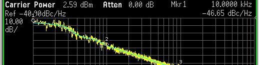


20 Measurement results Phase Noise measurements from 749MHz from 477MHz 20
21 Measurement results Tuning voltage effect on phase noise Results at 100KHz offset from carrier Measured results compare well with improved model Control Voltage Oscillation Theoretical Measurement Vninst(V) frequency Phase Noise Phase Noise f 0 (MHz) (dbc/hz) (dbc/hz)
22 Presentation outline Research motivation o Improved phase noise model Simulation results Measurement results Conclusions 22
23 Conclusions We have demonstrated that VCO tuning voltage does has an impact on phase noise performance. Existing phase noise models for differential delay cells have been extended to include this factor. The improved phase noise model has been shown to hold true over a large design space. Silicon prototype results indicate that the model can accurately predict the phase noise results. The proposed model has been built into a matlab model to reduce the design time of delay cell based VCOs. 23
24 Questions?

 749MHz 505MHz RMS 2.41ps 0.18% of period P-P 20.")

25 Measurement results Jitter summary Specification: Design Example 2 Supply voltage 1.2V Process 0.13µm(St120nm) Frequency range 197KHz-749MHz 749MHz Size 249µm 57µm Jitter (Measurement) 749MHz 505MHz RMS 2.41ps 0.18% of period P-P 20.49ps 1.5% of period RMS 1.95ps 0.099% 099% of period P-P 16.96ps 0.84% of period 48.1MHz RMS 8.75ps 0.042% of period P-P 84.26ps 0.4% of period 749MHz 24mW Power 505MHz 15.6mW 48.1MHz 2.98mW
AVoltage Controlled Oscillator (VCO) was designed and
 was designed and") 1 EECE 457 VCO Design Project Jason Khuu, Erik Wu Abstract This paper details the design and simulation of a Voltage Controlled Oscillator using a 0.13µm process. The final VCO design meets all specifications.
1 EECE 457 VCO Design Project Jason Khuu, Erik Wu Abstract This paper details the design and simulation of a Voltage Controlled Oscillator using a 0.13µm process. The final VCO design meets all specifications.
1P6M 0.18-µm Low Power CMOS Ring Oscillator for Radio Frequency Applications
 1P6M 0.18-µm Low Power CMOS Ring Oscillator for Radio Frequency Applications Ashish Raman and R. K. Sarin Abstract The monograph analysis a low power voltage controlled ring oscillator, implement using
A Low Phase Noise LC VCO for 6GHz
 A Low Phase Noise LC VCO for 6GHz Mostafa Yargholi 1, Abbas Nasri 2 Department of Electrical Engineering, University of Zanjan, Zanjan, Iran 1 yargholi@znu.ac.ir, 2 abbas.nasri@znu.ac.ir, Abstract: This
Design of VCOs in Global Foundries 28 nm HPP CMOS
 Design of VCOs in Global Foundries 28 nm HPP CMOS Evan Jorgensen 33 rd Annual Microelectronics Conference Rochester Institute of Technology Department of Electrical and Microelectronic Engineering May
A Low Noise, Voltage Control Ring Oscillator Based on Pass Transistor Delay Cell
 A Low Noise, Voltage Control Ring Oscillator Based on Pass Transistor Delay Cell Devi Singh Baghel 1, R.C. Gurjar 2 M.Tech Student, Department of Electronics and Instrumentation, Shri G.S. Institute of
ISSCC 2002 / SESSION 17 / ADVANCED RF TECHNIQUES / 17.2
 ISSCC 2002 / SESSION 17 / ADVANCED RF TECHNIQUES / 17.2 17.2 A CMOS Differential Noise-Shifting Colpitts VCO Roberto Aparicio, Ali Hajimiri California Institute of Technology, Pasadena, CA Demand for higher
Quadrature GPS Receiver Front-End in 0.13μm CMOS: The QLMV cell
 1 Quadrature GPS Receiver Front-End in 0.13μm CMOS: The QLMV cell Yee-Huan Ng, Po-Chia Lai, and Jia Ruan Abstract This paper presents a GPS receiver front end design that is based on the single-stage quadrature
A Multiobjective Optimization based Fast and Robust Design Methodology for Low Power and Low Phase Noise Current Starved VCO Gaurav Sharma 1
 IJSRD - International Journal for Scientific Research & Development Vol. 2, Issue 01, 2014 ISSN (online): 2321-0613 A Multiobjective Optimization based Fast and Robust Design Methodology for Low Power
HW#3 Solution. Dr. Parker. Spring 2014
 HW#3 olution r. Parker pring 2014 Assume for the problems below that V dd = 1.8 V, V tp0 is -.7 V. and V tn0 is.7 V. V tpbodyeffect is -.9 V. and V tnbodyeffect is.9 V. Assume ß n (k n )= 219.4 W/L µ A(microamps)/V
Analysis and Design of a Low phase noise, low power, Wideband CMOS Voltage Controlled Ring Oscillator in 90 nm process
 Analysis and Design of a Low phase noise, low power, Wideband CMOS Voltage Controlled Ring Oscillator in 90 nm process Sweta Padma Dash, Adyasha Rath, Geeta Pattnaik, Subhrajyoti Das, Anindita Dash Abstract
CMOS Current Starved Voltage Controlled Oscillator Circuit for a Fast Locking PLL
 IEEE INDICON 2015 1570186537 1 2 3 4 5 6 7 8 9 10 11 12 13 14 15 16 17 18 19 20 21 22 23 24 25 26 27 28 29 30 31 32 33 34 35 36 37 38 39 40 41 42 43 44 45 46 47 48 49 50 51 52 53 54 55 56 57 60 61 62 63
20 GHz Low Power QVCO and De-skew Techniques in 0.13µm Digital CMOS. Masum Hossain & Tony Chan Carusone University of Toronto
 20 GHz Low Power QVCO and De-skew Techniques in 0.13µm Digital CMOS Masum Hossain & Tony Chan Carusone University of Toronto masum@eecg.utoronto.ca Motivation Data Rx3 Rx2 D-FF D-FF Rx1 D-FF Clock Clock
ECE1352. Term Paper Low Voltage Phase-Locked Loop Design Technique
 ECE1352 Term Paper Low Voltage Phase-Locked Loop Design Technique Name: Eric Hu Student Number: 982123400 Date: Nov. 14, 2002 Table of Contents Abstract pg. 04 Chapter 1 Introduction.. pg. 04 Chapter 2
Chapter 5. Operational Amplifiers and Source Followers. 5.1 Operational Amplifier
 Chapter 5 Operational Amplifiers and Source Followers 5.1 Operational Amplifier In single ended operation the output is measured with respect to a fixed potential, usually ground, whereas in double-ended
Lecture 7: Components of Phase Locked Loop (PLL)
") Lecture 7: Components of Phase Locked Loop (PLL) CSCE 6933/5933 Instructor: Saraju P. Mohanty, Ph. D. NOTE: The figures, text etc included in slides are borrowed from various books, websites, authors pages,
Lecture 7: Components of Phase Locked Loop (PLL) CSCE 6933/5933 Instructor: Saraju P. Mohanty, Ph. D. NOTE: The figures, text etc included in slides are borrowed from various books, websites, authors pages,
Quiz2: Mixer and VCO Design
 Quiz2: Mixer and VCO Design Fei Sun and Hao Zhong 1 Question1 - Mixer Design 1.1 Design Criteria According to the specifications described in the problem, we can get the design criteria for mixer design:
Outline. Motivation. Design Challenges. Design of Mode-Switching VCO. Measurement Results. Conclusion 7/8/14
 Mazhareddin Taghivand, Kamal Aggarwal and Ada Poon Dept. of Electrical Engineering Stanford University Outline Motivation Design Challenges Design of Mode-Switching VCO Measurement Results Conclusion 2
ISSN:
 High Frequency Power Optimized Ring Voltage Controlled Oscillator for 65nm CMOS Technology NEHA K.MENDHE 1, M. N. THAKARE 2, G. D. KORDE 3 Department of EXTC, B.D.C.O.E, Sevagram, India, nehakmendhe02@gmail.com
A CMOS CURRENT CONTROLLED RING OSCILLATOR WITH WIDE AND LINEAR TUNING RANGE
 A CMOS CURRENT CONTROLLED RING OSCILLATOR WI WIDE AND LINEAR TUNING RANGE Abstract Ekachai Leelarasmee 1 1 Electrical Engineering Department, Chulalongkorn University, Bangkok 10330, Thailand Tel./Fax.
Integrated Circuit Amplifiers. Comparison of MOSFETs and BJTs
 Integrated Circuit Amplifiers Comparison of MOSFETs and BJTs 17 Typical CMOS Device Parameters 0.8 µm 0.25 µm 0.13 µm Parameter NMOS PMOS NMOS PMOS NMOS PMOS t ox (nm) 15 15 6 6 2.7 2.7 C ox (ff/µm 2 )
Analysis and Design of Low Power Ring Oscillators with Frequency ~ khz
 Analysis and Design of Low Power Ring Oscillators with Frequency ~10-100 khz PRESENTED BY: PIYUSH KESHRI 3 rd year Undergraduate Student Indian Institute Of Technology, Kanpur, India University Of Michigan
An Efficient Design of CMOS based Differential LC and VCO for ISM and WI-FI Band of Applications
 IJSTE - International Journal of Science Technology & Engineering Volume 2 Issue 10 April 2016 ISSN (online): 2349-784X An Efficient Design of CMOS based Differential LC and VCO for ISM and WI-FI Band
Designing and Simulation of Full Adder Cell using Self Reverse Biasing Technique
 Designing and Simulation of Full Adder Cell using Self Reverse Biasing Technique Chandni jain 1, Shipra mishra 2 1 M.tech. Embedded system & VLSI Design NITM,Gwalior M.P. India 474001 2 Asst Prof. EC Dept.,
A performance comparison of single ended and differential ring oscillator in 0.18 µm CMOS process
 A performance comparison of single ended and differential ring oscillator in 0.18 µm CMOS process Nadia Gargouri, Dalenda Ben Issa, Abdennaceur Kachouri & Mounir Samet Laboratory of Electronics and Technologies
Bootstrapped ring oscillator with feedforward inputs for ultra-low-voltage application
 This article has been accepted and published on J-STAGE in advance of copyediting. Content is final as presented. IEICE Electronics Express, Vol.* No.*,*-* Bootstrapped ring oscillator with feedforward
Design of Wide Tuning Range and Low Power Dissipation of VCRO in 50nm CMOS Technology
 Design of Wide Tuning Range and Low Power Dissipation of VCRO in 50nm CMOS Technology Gagandeep Singh 1, Mandeep Singh Angurana 2 PG Student, Dept. Of Microelectronics, BMS College of Engineering, Sri
Low Power, Wide Bandwidth Phase Locked Loop Design
 Low Power, Wide Bandwidth Phase Locked Loop Design Hariprasath Venkatram and Taehwan Oh Abstract A low power wide bandwidth phase locked loop is presented in the paper. The phase frequency detector, charge
NEW WIRELESS applications are emerging where
 IEEE JOURNAL OF SOLID-STATE CIRCUITS, VOL. 39, NO. 4, APRIL 2004 709 A Multiply-by-3 Coupled-Ring Oscillator for Low-Power Frequency Synthesis Shwetabh Verma, Member, IEEE, Junfeng Xu, and Thomas H. Lee,
Design of Low-Phase-Noise CMOS Ring Oscillators
 328 IEEE TRANSACTIONS ON CIRCUITS AND SYSTEMS II: ANALOG AND DIGITAL SIGNAL PROCESSING, VOL. 49, NO. 5, MAY 2002 Design of Low-Phase-Noise CMOS Ring Oscillators Liang Dai, Member, IEEE, and Ramesh Harjani,
Lecture 4. The CMOS Inverter. DC Transfer Curve: Load line. DC Operation: Voltage Transfer Characteristic. Noise in Digital Integrated Circuits
 Noise in Digital Integrated Circuits Lecture 4 The CMOS Inverter i(t) v(t) V DD Peter Cheung Department of Electrical & Electronic Engineering Imperial College London URL: www.ee.ic.ac.uk/pcheung/ E-mail:
Layout Design of LC VCO with Current Mirror Using 0.18 µm Technology
 Wireless Engineering and Technology, 2011, 2, 102106 doi:10.4236/wet.2011.22014 Published Online April 2011 (http://www.scirp.org/journal/wet) 99 Layout Design of LC VCO with Current Mirror Using 0.18
problem grade total
 Fall 2005 6.012 Microelectronic Devices and Circuits Prof. J. A. del Alamo Name: Recitation: November 16, 2005 Quiz #2 problem grade 1 2 3 4 total General guidelines (please read carefully before starting):
Design and Simulation of Low Voltage Operational Amplifier
 Design and Simulation of Low Voltage Operational Amplifier Zach Nelson Department of Electrical Engineering, University of Nevada, Las Vegas 4505 S Maryland Pkwy, Las Vegas, NV 89154 United States of America
A 45-nm SOI-CMOS Dual-PLL Processor Clock System for Multi-Protocol I/O
 A 45-nm SOI-CMOS Dual-PLL Processor Clock System for Multi-Protocol I/O Dennis Fischette, Alvin Loke, Michael Oshima, Bruce Doyle, Roland Bakalski*, Richard DeSantis, Anand Thiruvengadam, Charles Wang,
Design of Analog CMOS Integrated Circuits
 Design of Analog CMOS Integrated Circuits Behzad Razavi Professor of Electrical Engineering University of California, Los Angeles H Boston Burr Ridge, IL Dubuque, IA Madison, WI New York San Francisco
ISSN: International Journal of Engineering and Innovative Technology (IJEIT) Volume 1, Issue 2, February 2012
 Volume 1, Issue 2, February 2012") A Performance Comparison of Current Starved VCO and Source Coupled VCO for PLL in 0.18µm CMOS Process Rashmi K Patil, Vrushali G Nasre rashmikpatil@gmail.com, vrushnasre@gmail.com Abstract This paper describes
A Performance Comparison of Current Starved VCO and Source Coupled VCO for PLL in 0.18µm CMOS Process Rashmi K Patil, Vrushali G Nasre rashmikpatil@gmail.com, vrushnasre@gmail.com Abstract This paper describes
Introduction to VLSI ASIC Design and Technology
 Introduction to VLSI ASIC Design and Technology Paulo Moreira CERN - Geneva, Switzerland Paulo Moreira Introduction 1 Outline Introduction Is there a limit? Transistors CMOS building blocks Parasitics
Quadrature Generation Techniques in CMOS Relaxation Oscillators. S. Aniruddhan Indian Institute of Technology Madras Chennai, India
 Quadrature Generation Techniques in CMOS Relaxation Oscillators S. Aniruddhan Indian Institute of Technology Madras Chennai, India Outline Introduction & Motivation Quadrature Relaxation Oscillators (QRXO)
THE BASIC BUILDING BLOCKS OF 1.8 GHZ PLL
 THE BASIC BUILDING BLOCKS OF 1.8 GHZ PLL IN CMOS TECHNOLOGY L. Majer, M. Tomáška,V. Stopjaková, V. Nagy, and P. Malošek Department of Microelectronics, Slovak Technical University, Ilkovičova 3, Bratislava,
CHAPTER 3 CMOS LOW NOISE AMPLIFIERS
 46 CHAPTER 3 CMOS LOW NOISE AMPLIFIERS 3.1 INTRODUCTION The Low Noise Amplifier (LNA) plays an important role in the receiver design. LNA serves as the first block in the RF receiver. It is a critical
A Dual-Step-Mixing ILFD using a Direct Injection Technique for High- Order Division Ratios in 60GHz Applications
 A Dual-Step-Mixing ILFD using a Direct Injection Technique for High- Order Division Ratios in 60GHz Applications Teerachot Siriburanon, Wei Deng, Ahmed Musa, Kenichi Okada, and Akira Matsuzawa Tokyo Institute
Low Voltage CMOS VCOs
 Competence Center for Circuit Design Low Voltage CMOS VCOs Niklas Troedsson Niklas.Troedsson@es.lth.se Department of Electroscience Lund Institute of Technology Lund University Sweden Niklas Troedsson.
An Analog Phase-Locked Loop
 1 An Analog Phase-Locked Loop Greg Flewelling ABSTRACT This report discusses the design, simulation, and layout of an Analog Phase-Locked Loop (APLL). The circuit consists of five major parts: A differential
A 2.4 GHZ RECEIVER IN SILICON-ON-SAPPHIRE MICHAEL PETERS. B.S., Kansas State University, 2009 A REPORT
 A 2.4 GHZ RECEIVER IN SILICON-ON-SAPPHIRE by MICHAEL PETERS B.S., Kansas State University, 2009 A REPORT submitted in partial fulfillment of the requirements for the degree MASTER OF SCIENCE Department
HW#3 Solution. Dr. Parker. Fall 2015
 HW#3 Solution Dr. Parker Fall 2015 Assume for the problems below that V dd = 1.8 V, V tp0 is -.7 V. and V tn0 is.7 V. V tpbodyeffect is -.9 V. and V tnbodyeffect is.9 V. Assume ß n (k n )= 219.4 W/L µ
Hot Topics and Cool Ideas in Scaled CMOS Analog Design
 Engineering Insights 2006 Hot Topics and Cool Ideas in Scaled CMOS Analog Design C. Patrick Yue ECE, UCSB October 27, 2006 Slide 1 Our Research Focus High-speed analog and RF circuits Device modeling,
Low Power High Performance 10T Full Adder for Low Voltage CMOS Technology Using Dual Threshold Voltage
 Low Power High Performance 10T Full Adder for Low Voltage CMOS Technology Using Dual Threshold Voltage Surbhi Kushwah 1, Shipra Mishra 2 1 M.Tech. VLSI Design, NITM College Gwalior M.P. India 474001 2
Ping Gui, Member, IEEE, Peiqing Zhu, Wickham Chen, Student Member, IEEE, Dennis Wu, Sungyong Jung, Senior Member, IEEE
 > REPLACE THIS LINE WITH YOUR PAPER IDENTIFICATION NUMBER (DOUBLE-CLICK HERE TO EDIT) < 1 A TID Tolerant, Wide Band and Low Jitter Phase-Locked Loop in 0.25 m CMOS Silicon-on-Sapphire Technology Ping Gui,
DESIGN AND PERFORMANCE VERIFICATION OF CURRENT CONVEYOR BASED PIPELINE A/D CONVERTER USING 180 NM TECHNOLOGY
 DESIGN AND PERFORMANCE VERIFICATION OF CURRENT CONVEYOR BASED PIPELINE A/D CONVERTER USING 180 NM TECHNOLOGY Neha Bakawale Departmentof Electronics & Instrumentation Engineering, Shri G. S. Institute of
DESIGN OF LOW-VOLTAGE WIDE TUNING RANGE CMOS MULTIPASS VOLTAGE-CONTROLLED RING OSCILLATOR
 DESIGN OF LOW-VOLTAGE WIDE TUNING RANGE CMOS MULTIPASS VOLTAGE-CONTROLLED RING OSCILLATOR by Jie Ren Submitted in partial fulfilment of the requirements for the degree of Master of Applied Science at Dalhousie
A Low-Offset Latched Comparator Using Zero-Static Power Dynamic Offset Cancellation Technique
 1 A Low-Offset Latched Comparator Using Zero-Static Power Dynamic Offset Cancellation Technique Masaya Miyahara and Akira Matsuzawa Tokyo Institute of Technology, Japan 2 Outline Motivation Design Concept
Metal Oxide Semiconductor Field-Effect Transistors (MOSFETs)
") Metal Oxide Semiconductor Field-Effect Transistors (MOSFETs) Device Structure N-Channel MOSFET Providing electrons Pulling electrons (makes current flow) + + + Apply positive voltage to gate: Drives away
Metal Oxide Semiconductor Field-Effect Transistors (MOSFETs) Device Structure N-Channel MOSFET Providing electrons Pulling electrons (makes current flow) + + + Apply positive voltage to gate: Drives away
Low Power Realization of Subthreshold Digital Logic Circuits using Body Bias Technique
 Indian Journal of Science and Technology, Vol 9(5), DOI: 1017485/ijst/2016/v9i5/87178, Februaru 2016 ISSN (Print) : 0974-6846 ISSN (Online) : 0974-5645 Low Power Realization of Subthreshold Digital Logic
A 0.2-to-1.45GHz Subsampling Fractional-N All-Digital MDLL with Zero-Offset Aperture PD-Based Spur Cancellation and In-Situ Timing Mismatch Detection
 A 0.2-to-1.45GHz Subsampling Fractional-N All-Digital MDLL with Zero-Offset Aperture PD-Based Spur Cancellation and In-Situ Timing Mismatch Detection Somnath Kundu 1, Bongjin Kim 1,2, Chris H. Kim 1 1
A Low-Jitter Phase-Locked Loop Based on a Charge Pump Using a Current-Bypass Technique
 JOURNAL OF SEMICONDUCTOR TECHNOLOGY AND SCIENCE, VOL.14, NO.3, JUNE, 2014 http://dx.doi.org/10.5573/jsts.2014.14.3.331 A Low-Jitter Phase-Locked Loop Based on a Charge Pump Using a Current-Bypass Technique
Project #2 for Electronic Circuit II
 Project #2 for Electronic Circuit II Prof. Woo-Young Choi TA: Hyunkyu Kim, Minkyu Kim June 7, 2017 - Deadline : 6:00 pm on June 23, 2017. Penalties for late hand-in. - Team Students are expected to form
All Digital on Chip Process Sensor Using Ratioed Inverter Based Ring Oscillator
 All Digital on Chip Process Sensor Using Ratioed Inverter Based Ring Oscillator 1 G. Rajesh, 2 G. Guru Prakash, 3 M.Yachendra, 4 O.Venka babu, 5 Mr. G. Kiran Kumar 1,2,3,4 Final year, B. Tech, Department
A Low-Noise Self-Calibrating Dynamic Comparator for High-Speed ADCs
 1 A Low-Noise Self-Calibrating Dynamic Comparator for High-Speed ADCs Masaya Miyahara, Yusuke Asada, Daehwa Paik and Akira Matsuzawa Tokyo Institute of Technology, Japan Outline 2 Motivation The Calibration
DESIGNING A NEW RING OSCILLATOR FOR HIGH PERFORMANCE APPLICATIONS IN 65nm CMOS TECHNOLOGY
 DESIGNING A NEW RING OSCILLATOR FOR HIGH PERFORMANCE APPLICATIONS IN 65nm CMOS TECHNOLOGY *Yusuf Jameh Bozorg and Mohammad Jafar Taghizadeh Marvast Department of Electrical Engineering, Mehriz Branch,
A 2.6GHz/5.2GHz CMOS Voltage-Controlled Oscillator*
 WP 23.6 A 2.6GHz/5.2GHz CMOS Voltage-Controlled Oscillator* Christopher Lam, Behzad Razavi University of California, Los Angeles, CA New wireless local area network (WLAN) standards have recently emerged
A PSEUDO-CLASS-AB TELESCOPIC-CASCODE OPERATIONAL AMPLIFIER
 A PSEUDO-CLASS-AB TELESCOPIC-CASCODE OPERATIONAL AMPLIFIER M. Taherzadeh-Sani, R. Lotfi, and O. Shoaei ABSTRACT A novel class-ab architecture for single-stage operational amplifiers is presented. The structure
Design and power optimization of CMOS RF blocks operating in the moderate inversion region
 Design and power optimization of CMOS RF blocks operating in the moderate inversion region Leonardo Barboni, Rafaella Fiorelli, Fernando Silveira Instituto de Ingeniería Eléctrica Facultad de Ingeniería
Low Power Wide Frequency Range Current Starved CMOS VCO in 180nm, 130nm and 90nm CMOS Technology
 International Journal of Engineering Research and Development e-issn: 2278-067X, p-issn: 2278-800X, www.ijerd.com Volume 7, Issue 4 (May 2013), PP. 80-84 Low Power Wide Frequency Range Current Starved
Lecture 300 Low Voltage Op Amps (3/28/10) Page 300-1
 Page 300-1") Lecture 300 Low Voltage Op Amps (3/28/10) Page 300-1 LECTURE 300 LOW VOLTAGE OP AMPS LECTURE ORGANIZATION Outline Introduction Low voltage input stages Low voltage gain stages Low voltage bias circuits
Lecture 300 Low Voltage Op Amps (3/28/10) Page 300-1 LECTURE 300 LOW VOLTAGE OP AMPS LECTURE ORGANIZATION Outline Introduction Low voltage input stages Low voltage gain stages Low voltage bias circuits
A 2.4 GHz to 3.86 GHz digitally controlled oscillator with 18.5 khz frequency resolution using single PMOS varactor
 LETTER IEICE Electronics Express, Vol.9, No.24, 1842 1848 A 2.4 GHz to 3.86 GHz digitally controlled oscillator with 18.5 khz frequency resolution using single PMOS varactor Yangyang Niu, Wei Li a), Ning
Efficient VCO using FinFET
 Indian Journal of Science and Technology, Vol 8(S2), 262 270, January 2015 ISSN (Print) : 0974-6846 ISSN (Online) : 0974-5645 DOI:.10.17485/ijst/2015/v8iS2/67807 Efficient VCO using FinFET Siddharth Saxena
Lecture 160 Examples of CDR Circuits in CMOS (09/04/03) Page 160-1
 Page 160-1") Lecture 160 Examples of CDR Circuits in CMOS (09/04/03) Page 160-1 LECTURE 160 CDR EXAMPLES INTRODUCTION Objective The objective of this presentation is: 1.) Show two examples of clock and data recovery
Lecture 160 Examples of CDR Circuits in CMOS (09/04/03) Page 160-1 LECTURE 160 CDR EXAMPLES INTRODUCTION Objective The objective of this presentation is: 1.) Show two examples of clock and data recovery
Analysis of 1=f Noise in CMOS Preamplifier With CDS Circuit
 IEEE TRANSACTIONS ON NUCLEAR SCIENCE, VOL. 49, NO. 4, AUGUST 2002 1819 Analysis of 1=f Noise in CMOS Preamplifier With CDS Circuit Tae-Hoon Lee, Gyuseong Cho, Hee Joon Kim, Seung Wook Lee, Wanno Lee, and
/$ IEEE
 IEEE TRANSACTIONS ON CIRCUITS AND SYSTEMS II: EXPRESS BRIEFS, VOL. 53, NO. 11, NOVEMBER 2006 1205 A Low-Phase Noise, Anti-Harmonic Programmable DLL Frequency Multiplier With Period Error Compensation for
Design of a Low Noise Amplifier using 0.18µm CMOS technology
 The International Journal Of Engineering And Science (IJES) Volume 4 Issue 6 Pages PP.11-16 June - 2015 ISSN (e): 2319 1813 ISSN (p): 2319 1805 Design of a Low Noise Amplifier using 0.18µm CMOS technology
A 3 8 GHz Broadband Low Power Mixer
 PIERS ONLINE, VOL. 4, NO. 3, 8 361 A 3 8 GHz Broadband Low Power Mixer Chih-Hau Chen and Christina F. Jou Institute of Communication Engineering, National Chiao Tung University, Hsinchu, Taiwan Abstract
ECEN 474/704 Lab 6: Differential Pairs
 ECEN 474/704 Lab 6: Differential Pairs Objective Design, simulate and layout various differential pairs used in different types of differential amplifiers such as operational transconductance amplifiers
School of Electronics, Devi Ahilya University, Indore, Madhya Pradesh, India 3. Acropolis Technical Campus, Indore, Madhya Pradesh, India
 International Journal of Emerging Research in Management &Technology Research Article August 2017 Power Efficient Implementation of Low Noise CMOS LC VCO using 32nm Technology for RF Applications 1 Shitesh
SP 23.6: A 1.8GHz CMOS Voltage-Controlled Oscillator
 SP 23.6: A 1.8GHz CMOS Voltage-Controlled Oscillator Behzad Razavi University of California, Los Angeles, CA Formerly with Hewlett-Packard Laboratories, Palo Alto, CA This paper describes the factors that
SiNANO-NEREID Workshop:
 SiNANO-NEREID Workshop: Towards a new NanoElectronics Roadmap for Europe Leuven, September 11 th, 2017 WP3/Task 3.2 Connectivity RF and mmw Design Outline Connectivity, what connectivity? High data rates
Project #3 for Electronic Circuit II
 Project #3 for Electronic Circuit II Prof. Woo-Young Choi TA: Tongsung Kim, Minkyu Kim June 1, 2015 - Deadline : 6:00 pm on June 22, 2015. Penalties for late hand-in. - Team Students are expected to form
Conference Guide IEEE International Symposium on Circuits and Systems. Rio de Janeiro, May 15 18, 2011
 2011 IEEE International Symposium on Circuits and Systems Rio de Janeiro, May 15 18, 2011 Conference Guide The Institute of Electrical and Eletronics Engineers IEEE Circuits and System s Society Federal
DESIGN OF CMOS BASED FM MODULATOR USING 90NM TECHNOLOGY ON CADENCE VIRTUOSO TOOL
 DESIGN OF CMOS BASED FM MODULATOR USING 90NM TECHNOLOGY ON CADENCE VIRTUOSO TOOL 1 Parmjeet Singh, 2 Rekha Yadav, 1, 2 Electronics and Communication Engineering Department D.C.R.U.S.T. Murthal, 1, 2 Sonepat,
A NOVEL ARCHITECTURE FOR SUPPLY-REGULATED VOLTAGE-CONTROLLED OSCILLATORS
 A NOVEL ARCHITECTURE FOR SUPPLY-REGULATED VOLTAGE-CONTROLLED OSCILLATORS A Thesis Presented in Partial Fulfillment of the Requirements for the Degree Master of Science in the Graduate School of The Ohio
An Optimal Design of Ring Oscillator and Differential LC using 45 nm CMOS Technology
 IJIRST International Journal for Innovative Research in Science & Technology Volume 2 Issue 10 March 2016 ISSN (online): 2349-6010 An Optimal Design of Ring Oscillator and Differential LC using 45 nm CMOS
Lecture 16. Complementary metal oxide semiconductor (CMOS) CMOS 1-1
 CMOS 1-1") Lecture 16 Complementary metal oxide semiconductor (CMOS) CMOS 1-1 Outline Complementary metal oxide semiconductor (CMOS) Inverting circuit Properties Operating points Propagation delay Power dissipation
Lecture 16 Complementary metal oxide semiconductor (CMOS) CMOS 1-1 Outline Complementary metal oxide semiconductor (CMOS) Inverting circuit Properties Operating points Propagation delay Power dissipation
A RF Low Power 0.18-µm based CMOS Differential Ring Oscillator
 , July 4-6, 2012, London, U.K. A RF Low Power 0.18-µm based CMOS Differential Ring Oscillator Ashish Raman 1,Jaya Nidhi Vashishtha 1 and R K sarin 2 Abstract A voltage controlled ring oscillator is implemented
Michael S. McCorquodale, Ph.D. Founder and CTO, Mobius Microsystems, Inc.
 Self-Referenced, Trimmed and Compensated RF CMOS Harmonic Oscillators as Monolithic Frequency Generators Integrating Time Michael S. McCorquodale, Ph.D. Founder and CTO, Mobius Microsystems, Inc. 2008
A 484µm 2, 21GHz LC-VCO Beneath a Stacked-Spiral Inductor
 A 484µm, GHz LC-VCO Beneath a Stacked-Spiral Inductor Rui Murakami, Kenichi Okada, and Akira Tokyo Institute of Technology, Japan 00/09/8 Contents Background Downsizing of LC-VCO Circuit Stacking Beneath
Fin-Shaped Field Effect Transistor (FinFET) Min Ku Kim 03/07/2018
 Min Ku Kim 03/07/2018") Fin-Shaped Field Effect Transistor (FinFET) Min Ku Kim 03/07/2018 ECE 658 Sp 2018 Semiconductor Materials and Device Characterizations OUTLINE Background FinFET Future Roadmap Keeping up w/ Moore s Law
Fin-Shaped Field Effect Transistor (FinFET) Min Ku Kim 03/07/2018 ECE 658 Sp 2018 Semiconductor Materials and Device Characterizations OUTLINE Background FinFET Future Roadmap Keeping up w/ Moore s Law
High Performance Digital Fractional-N Frequency Synthesizers
 High Performance Digital Fractional-N Frequency Synthesizers Michael Perrott October 16, 2008 Copyright 2008 by Michael H. Perrott All rights reserved. Why Are Digital Phase-Locked Loops Interesting? PLLs
Low Flicker Noise Current-Folded Mixer
 Chapter 4 Low Flicker Noise Current-Folded Mixer The chapter presents a current-folded mixer achieving low 1/f noise for low power direct conversion receivers. Section 4.1 introduces the necessity of low
A fully synthesizable injection-locked PLL with feedback current output DAC in 28 nm FDSOI
 LETTER IEICE Electronics Express, Vol.1, No.15, 1 11 A fully synthesizable injection-locked PLL with feedback current output DAC in 8 nm FDSOI Dongsheng Yang a), Wei Deng, Aravind Tharayil Narayanan, Rui
DESIGN OF CMOS BASED FM QUADRATURE DEMODULATOR USING 45NM TECHNOLOGY
 DESIGN OF CMOS BASED FM QUADRATURE DEMODULATOR USING 45NM TECHNOLOGY 1 Pardeep Kumar, 2 Rekha Yadav, 1, 2 Electronics and Communication Engineering Department D.C.R.U.S.T. Murthal, 1, 2 Sonepat, 1, 2 Haryana,
Keywords Divide by-4, Direct injection, Injection locked frequency divider (ILFD), Low voltage, Locking range.
, Low voltage, Locking range.") Volume 6, Issue 4, April 2016 ISSN: 2277 128X International Journal of Advanced Research in Computer Science and Software Engineering Research Paper Available online at: www.ijarcsse.com Design of CMOS
Volume 6, Issue 4, April 2016 ISSN: 2277 128X International Journal of Advanced Research in Computer Science and Software Engineering Research Paper Available online at: www.ijarcsse.com Design of CMOS
A 2.4GHz Fully Integrated CMOS Power Amplifier Using Capacitive Cross-Coupling
 A 2.4GHz Fully Integrated CMOS Power Amplifier Using Capacitive Cross-Coupling JeeYoung Hong, Daisuke Imanishi, Kenichi Okada, and Akira Tokyo Institute of Technology, Japan Contents 1 Introduction PA
IJSRD - International Journal for Scientific Research & Development Vol. 4, Issue 02, 2016 ISSN (online):
:") IJSRD - International Journal for Scientific Research & Development Vol. 4, Issue 02, 2016 ISSN (online): 2321-0613 Design & Analysis of CMOS Telescopic Operational Transconductance Amplifier (OTA) with
IJSRD - International Journal for Scientific Research & Development Vol. 4, Issue 02, 2016 ISSN (online): 2321-0613 Design & Analysis of CMOS Telescopic Operational Transconductance Amplifier (OTA) with
ISSCC 2004 / SESSION 21/ 21.1
 ISSCC 2004 / SESSION 21/ 21.1 21.1 Circular-Geometry Oscillators R. Aparicio, A. Hajimiri California Institute of Technology, Pasadena, CA Demand for faster data rates in wireline and wireless markets
Design of a 3.3-V 1-GHz CMOS Phase Locked Loop with a Two-Stage Self-Feedback Ring Oscillator
 Journal of the Korean Physical Society, Vol. 37, No. 6, December 2000, pp. 803 807 Design of a 3.3-V 1-GHz CMOS Phase Locked Loop with a Two-Stage Self-Feedback Ring Oscillator Yeon Kug Moon Korea Advanced
A 10-GHz CMOS LC VCO with Wide Tuning Range Using Capacitive Degeneration
 JOURNAL OF SEMICONDUCTOR TECHNOLOGY AND SCIENCE, VOL.6, NO.4, DECEMBER, 2006 281 A 10-GHz CMOS LC VCO with Wide Tuning Range Using Capacitive Degeneration Tae-Geun Yu, Seong-Ik Cho, and Hang-Geun Jeong
ECE 442 Solid State Devices & Circuits. 15. Differential Amplifiers
 ECE 442 Solid State Devices & Circuits 15. Differential Amplifiers Jose E. Schutt-Aine Electrical & Computer Engineering University of Illinois jschutt@emlab.uiuc.edu ECE 442 Jose Schutt Aine 1 Background
Enhancement of VCO linearity and phase noise by implementing frequency locked loop
 Enhancement of VCO linearity and phase noise by implementing frequency locked loop Abstract This paper investigates the on-chip implementation of a frequency locked loop (FLL) over a VCO that decreases
REDUCING power consumption and enhancing energy
 548 IEEE TRANSACTIONS ON CIRCUITS AND SYSTEMS II: EXPRESS BRIEFS, VOL. 63, NO. 6, JUNE 2016 A Low-Voltage PLL With a Supply-Noise Compensated Feedforward Ring VCO Sung-Geun Kim, Jinsoo Rhim, Student Member,
Due to the absence of internal nodes, inverter-based Gm-C filters [1,2] allow achieving bandwidths beyond what is possible
![Due to the absence of internal nodes, inverter-based Gm-C filters [1,2] allow achieving bandwidths beyond what is possible](/thumbs/73/68507481.jpg "Due to the absence of internal nodes, inverter-based Gm-C filters [1,2] allow achieving bandwidths beyond what is possible") A Forward-Body-Bias Tuned 450MHz Gm-C 3 rd -Order Low-Pass Filter in 28nm UTBB FD-SOI with >1dBVp IIP3 over a 0.7-to-1V Supply Joeri Lechevallier 1,2, Remko Struiksma 1, Hani Sherry 2, Andreia Cathelin
A Forward-Body-Bias Tuned 450MHz Gm-C 3 rd -Order Low-Pass Filter in 28nm UTBB FD-SOI with >1dBVp IIP3 over a 0.7-to-1V Supply Joeri Lechevallier 1,2, Remko Struiksma 1, Hani Sherry 2, Andreia Cathelin
A LOW POWER, HIGH DYNAMIC RANGE, BROADBAND VARIABLE GAIN AMPLIFIER FOR AN ULTRA WIDEBAND RECEIVER. A Thesis LIN CHEN
 A LOW POWER, HIGH DYNAMIC RANGE, BROADBAND VARIABLE GAIN AMPLIFIER FOR AN ULTRA WIDEBAND RECEIVER A Thesis by LIN CHEN Submitted to the Office of Graduate Studies of Texas A&M University in partial fulfillment