Mask projection surface structuring
|
|
|
- Lenard Rose
- 5 years ago
- Views:
Transcription


1 Willkommen Welcome Bienvenue Mask projection surface structuring Patrik Hoffmann Advanced Materials Processing Empa Thun, Switzerland EPHJ - Geneva,
2 Outline Ablation process - limitations Excimer lasers Installation in Thun Examples
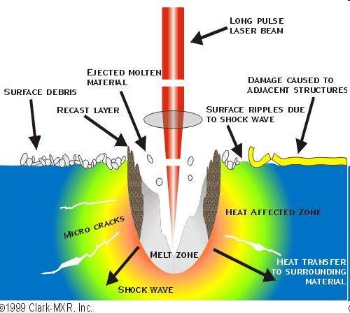
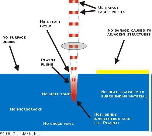
3 ns-machining vs. fs-machining ns fs

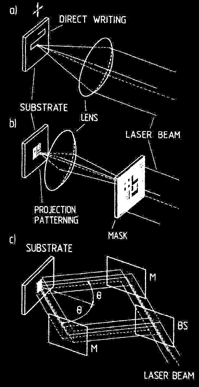
4 Different exposure of light
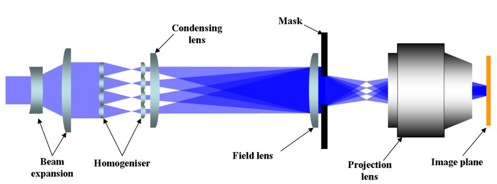
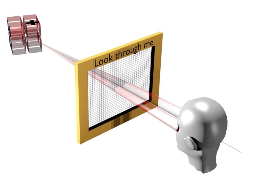
5 Mask projection system
6 Focus control - resolution and N.A. f# = u / d f/10 d ø sinø = NA u / d = 10 Diffraction Resolution Limit = k l NA k=0.8 NA=0.1 l=248 nm Res. limit = 2 µm k=0.6 NA=0.85 l=193 nm Res. limit = 136 nm u NA 1 / 2f# Depth of field D of F = l NA 2 NA=0.1 l=248 nm dof = 25 µm (±12 µm) NA=0.85 l=193 nm dof = 270 nm (±135 nm)
7 What happens at Empa Thun?

8 Full process


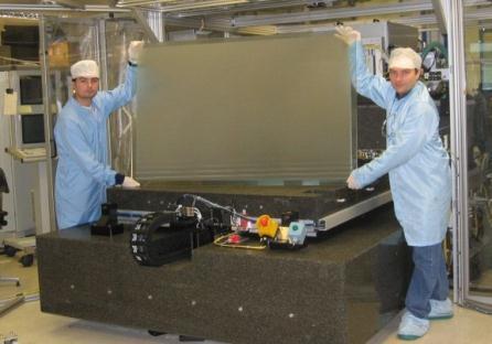
9 XL Micromachining System Travel 400 mm Accuracy ±0.50 µm Repeatability ±0.20 µm Straightness Flatness ±0.40µm ±0.40µm


10 XXL microprocessing machine Some highlights 3 m 2 exposure area Ultra high precision: x/y axis < 40 nm resolution (laser interferometer based encoders) Repeatability 3 um over full travel (+/- 1.5 ppm)
11 Advanced mask imaging Projection ablation options for complex surface shapes Variable aperture mask Scanned mask &/or workpiece Gray scale mask
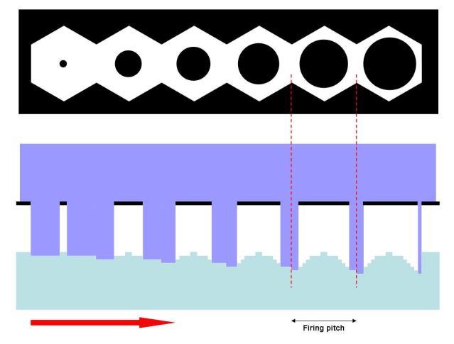

12 Synchronized Image Scanning (SIS)


13 Intensity modulation of the imaged pattern 1mm 1µm holes Depth information incorporated in half-tone mask Transmission varied by changing hole size or density 8-level Diffractive Optical Element Material: Polycarbonate; Laser: KrF excimer 248nm; Optics: x5, 0.13NA;
14 What can be & has been done with our systems?

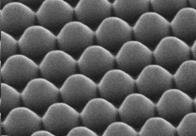
15 Wide range of materials can be ablated Polymers Metals Glasses Silicon Optical materials Composites Ceramics Thin films Courtesy of LML UK

 Time-of-flight mass")
 Micro tip Material sample")
16 Laser machining of ceramics Schematic of one part of Scanning Atom Probe Instrument (SAP) Time-of-flight mass spectrometer Electrode (Al 2 O 3 ) Micro tip Material sample 248nm (KrF) 10J/cm2


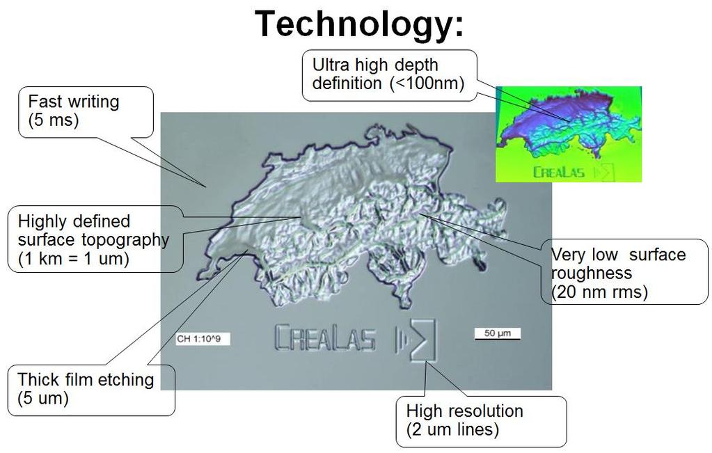
17 Microstructures in green ceramics 1/50 of energy density needed to machine Potential for highly efficient micro structuring of ceramics Green zirconia powder pressed and laser ablated after sintering Courtesy of EPFL


18 Laser machining of polymers Low ablation threshold (< 100 mj/cm 2 ) Low surface roughness High edge definition ~ 1 um resolution


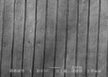
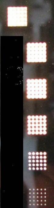
19 Mask imaging from submicron to millimetre feature 1 µm 10 µm 100 µm 1000 µm


20 Feature quality: fit of target shape The average deviation from the best fit ROC is 147 nm with a ROC of 59.2 μm while the target is 60 μm.

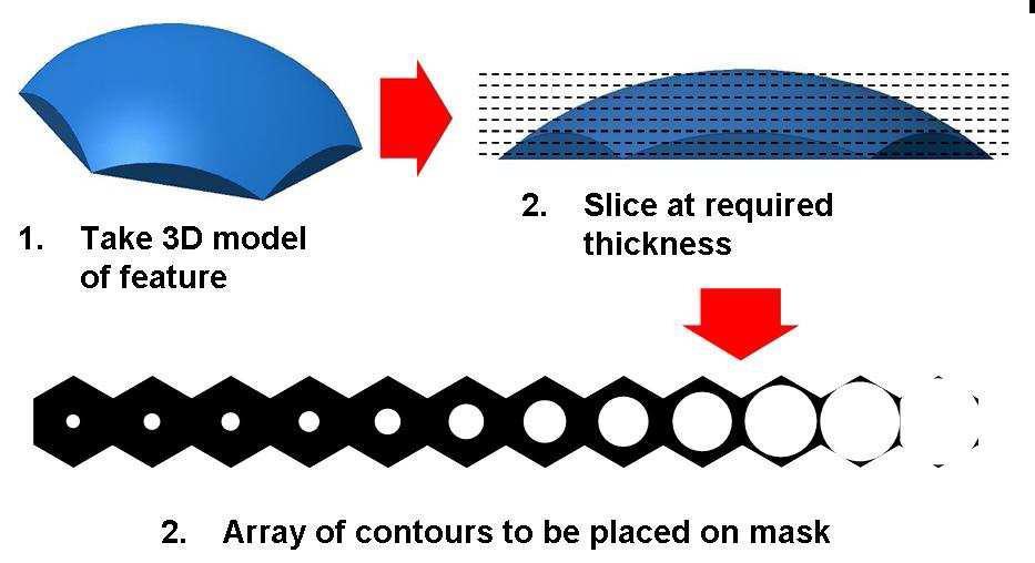
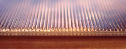
21 Examples Individual feature size x/y: 2 µm 1000 µm Feature height or depth z: µm Wall angles and slopes α: 0 85


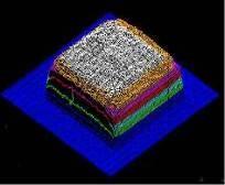
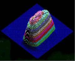
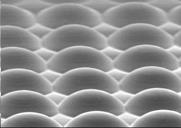
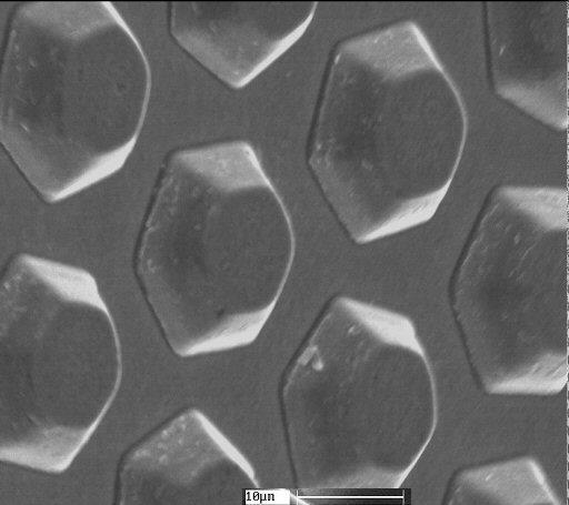
22 Large surface replication Laser cut Microlens array DHM measured ᴓ = 70 µm, h = 25 µm LAMP - Team: Dr Karl Böhlen, Mr Erdem Siringil, Dr Kilian Wasmer


23 Gradients of structures Bio-platform of advanced micro-topographical surface Existing Structures taken from Materiomics => 2.5D, principleinvestigators/jandeboer/res earch Laser Center Thun Exitech PPM601E capability of micro-structuring very large areas up to 1900 x 1450mm 2. Full 3D-structure with grandient The colour indicates the circles diameter. The pitch increases with the angle. The scales unity is [μm] Or R = f r R = f r g θ LAMP - Team: Dr Karl Böhlen, Mr Erdem Siringil, Dr Valentina Dinca, Dr Kilian Wasmer

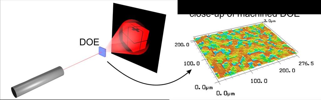


24 DOE Diffractive Optical Elements Optical function Computed DOE Iterative algorithm Left eye -2 Right eye +2


25 Characterization of phase elements Diffractive optical element (DOE) mm mm Phase maps mm DHM of 8-levels DOE : unit element 5x5mm 2 20x 50x
26


27 Applications 3 D TV: Large area precision masters


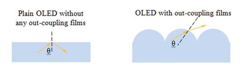
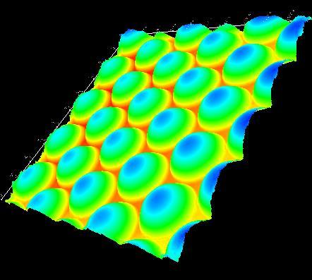
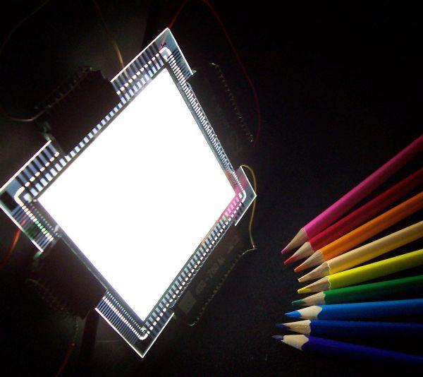
28 Applications Keyboard illumination: OLED out-coupling:


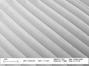
29 Applications Advanced surfaces Biomimic surfaces (Lotus, Gecko, etc) Friction and drag reduced surfaces Selectively activated (e.g. hydrophilic & hydrophobic) 2 um
 Friction and drag reduced surfaces Selectively activated")

30 Applications Advanced surfaces Biomimic surfaces (Lotus, Gecko, etc) Friction and drag reduced surfaces Selectively activated (hydrophilic & hydrophobic) James F. Schumacher et. al, Langmuir 2008, 24, Kenneth K. Chung et. al, Biointerphases, 2007, 2, 89-94

31 Conclusions Large surface laser processing possible Master pieces - replication
SNAPP Swiss National Applicaton Laboratory for Photonic tools and Photonic manufacturing
 SNAPP Swiss National Applicaton Laboratory for Photonic tools and Photonic manufacturing Details of SNAPP Look into the laboratories of the partner Swiss National Photonics Labs SNAPP Swiss National Applicaton
Excimer laser projector for microelectronics applications
 Excimer laser projector for microelectronics applications P T Rumsby and M C Gower Exitech Ltd Hanborough Park, Long Hanborough, Oxford OX8 8LH, England ABSTRACT Fully integrated excimer laser mask macro
Pulsed Laser Ablation of Polymers for Display Applications
 Pulsed Laser Ablation of Polymers for Display Applications James E.A Pedder 1, Andrew S. Holmes 2, Heather J. Booth 1 1 Oerlikon Optics UK Ltd, Oxford Industrial Estate, Yarnton, Oxford, OX5 1QU, UK 2
New techniques for laser micromachining MEMS devices
 New techniques for laser micromachining MEMS devices Charles Abbott, Ric Allott, Bob Bann, Karl Boehlen, Malcolm Gower, Phil Rumsby, Ines Stassen- Boehlen and Neil Sykes Exitech Ltd, Oxford Industrial
Lithography. 3 rd. lecture: introduction. Prof. Yosi Shacham-Diamand. Fall 2004
 Lithography 3 rd lecture: introduction Prof. Yosi Shacham-Diamand Fall 2004 1 List of content Fundamental principles Characteristics parameters Exposure systems 2 Fundamental principles Aerial Image Exposure
Advances in Laser Micro-machining for Wafer Probing and Trimming
 Advances in Laser Micro-machining for Wafer Probing and Trimming M.R.H. Knowles, A.I.Bell, G. Rutterford & A. Webb Oxford Lasers June 10, 2002 Oxford Lasers June 2002 1 Introduction to Laser Micro-machining
MICRO-ENGINEERING APPLICATIONS OF PULSED LASERS
 MICRO-ENGINEERING APPLICATIONS OF PULSED LASERS Nadeem Rizvi Exitech Limited Hanborough Park, Long Hanborough, Oxford OX8 8LH, United Kingdom. INTRODUCTION Lasers are currently being used world-wide in
Laser micro-machining of high density optical structures on large substrates
 Laser micro-machining of high density optical structures on large substrates Karl L. Boehlen*, Ines B. Stassen Boehlen Exitech Ltd, Oxford Industrial Park, Yarnton, Oxford, OX5 1QU, United Kingdom ABSTRACT
UV EXCIMER LASER BEAM HOMOGENIZATION FOR MICROMACHINING APPLICATIONS
 Optics and Photonics Letters Vol. 4, No. 2 (2011) 75 81 c World Scientific Publishing Company DOI: 10.1142/S1793528811000226 UV EXCIMER LASER BEAM HOMOGENIZATION FOR MICROMACHINING APPLICATIONS ANDREW
Laser Processing for the Fabrication of MEMS Devices
 Laser Processing for the Fabrication of MEMS Devices Andrew S. Holmes Optical & Semiconductor Devices Group Department of Electrical & Electronic Engineering Imperial College, London SW7 2AZ, UK a.holmes@imperial.ac.uk
Figure 7 Dynamic range expansion of Shack- Hartmann sensor using a spatial-light modulator
 Figure 4 Advantage of having smaller focal spot on CCD with super-fine pixels: Larger focal point compromises the sensitivity, spatial resolution, and accuracy. Figure 1 Typical microlens array for Shack-Hartmann
The Laser Processing of Diamond and Sapphire
 The Laser Processing of Diamond and Sapphire Neil Sykes Micronanics Limited neil@micronanics.com Diamond Diamond has the highest hardness and thermal conductivity of any bulk material 10/10 on the Mohs
A BASIC EXPERIMENTAL STUDY OF CAST FILM EXTRUSION PROCESS FOR FABRICATION OF PLASTIC MICROLENS ARRAY DEVICE
 A BASIC EXPERIMENTAL STUDY OF CAST FILM EXTRUSION PROCESS FOR FABRICATION OF PLASTIC MICROLENS ARRAY DEVICE Chih-Yuan Chang and Yi-Min Hsieh and Xuan-Hao Hsu Department of Mold and Die Engineering, National
Multi-aperture camera module with 720presolution
 Multi-aperture camera module with 720presolution using microoptics A. Brückner, A. Oberdörster, J. Dunkel, A. Reimann, F. Wippermann, A. Bräuer Fraunhofer Institute for Applied Optics and Precision Engineering
Optical Lithography. Keeho Kim Nano Team / R&D DongbuAnam Semi
 Optical Lithography Keeho Kim Nano Team / R&D DongbuAnam Semi Contents Lithography = Photolithography = Optical Lithography CD : Critical Dimension Resist Pattern after Development Exposure Contents Optical
ICMIEE Generation of Various Micropattern Using Microlens Projection Photolithography
 International Conference on Mechanical, Industrial and Energy Engineering 2014 26-27 December, 2014, Khulna, BANGLADESH Generation of Various Micropattern Using Microlens Projection Photolithography Md.
Femtosecond laser microfabrication in. Prof. Dr. Cleber R. Mendonca
 Femtosecond laser microfabrication in polymers Prof. Dr. Cleber R. Mendonca laser microfabrication focus laser beam on material s surface laser microfabrication laser microfabrication laser microfabrication
Micro- and Nano-Technology... for Optics
 Micro- and Nano-Technology...... for Optics 3.2 Lithography U.D. Zeitner Fraunhofer Institut für Angewandte Optik und Feinmechanik Jena Printing on Stones Map of Munich Stone Print Contact Printing light
Manufacturing Metrology Team
 The Team has a range of state-of-the-art equipment for the measurement of surface texture and form. We are happy to discuss potential measurement issues and collaborative research Manufacturing Metrology
MICROMACHINED INTERFEROMETER FOR MEMS METROLOGY
 MICROMACHINED INTERFEROMETER FOR MEMS METROLOGY Byungki Kim, H. Ali Razavi, F. Levent Degertekin, Thomas R. Kurfess G.W. Woodruff School of Mechanical Engineering, Georgia Institute of Technology, Atlanta,
Beam deflection technologies for ultra short pulse lasers June 5th, 2018
 Beam deflection technologies for ultra short pulse lasers June 5th, 2018 Agenda SCANLAB GmbH XL Scan excellishift precsys 2 SCANLAB at a Glance Worldwide leading OEM manufacturer of scan solutions for
Section 2: Lithography. Jaeger Chapter 2 Litho Reader. The lithographic process
 Section 2: Lithography Jaeger Chapter 2 Litho Reader The lithographic process Photolithographic Process (a) (b) (c) (d) (e) (f) (g) Substrate covered with silicon dioxide barrier layer Positive photoresist
Section 2: Lithography. Jaeger Chapter 2. EE143 Ali Javey Slide 5-1
 Section 2: Lithography Jaeger Chapter 2 EE143 Ali Javey Slide 5-1 The lithographic process EE143 Ali Javey Slide 5-2 Photolithographic Process (a) (b) (c) (d) (e) (f) (g) Substrate covered with silicon
Polissage et texturation de surface par fusion laser
 Polissage et texturation de surface par fusion laser Christophe ARNAUD, Anthony ALMIRALL, Charly LOUMENA et Rainer KLING C. Arnaud et al., Journal of Laser Applications, Vol. 29, 022501 (2017) Poste laser
Section 2: Lithography. Jaeger Chapter 2 Litho Reader. EE143 Ali Javey Slide 5-1
 Section 2: Lithography Jaeger Chapter 2 Litho Reader EE143 Ali Javey Slide 5-1 The lithographic process EE143 Ali Javey Slide 5-2 Photolithographic Process (a) (b) (c) (d) (e) (f) (g) Substrate covered
Sintec Optronics Pte Ltd Blk 134 Jurong East St 13 #04-309D Singapore Tel: (65) Fax:
 Fax:") Sintec Optronics Pte Ltd Blk 134 Jurong East St 13 #04-309D Singapore 600134 Tel: (65) 6862-7224 Fax: 6793-8060 E-mail: htinfo@singnet.com.sg Excimer laser drilling of polymers Y. H. Chen a, H. Y. Zheng
Sintec Optronics Pte Ltd Blk 134 Jurong East St 13 #04-309D Singapore 600134 Tel: (65) 6862-7224 Fax: 6793-8060 E-mail: htinfo@singnet.com.sg Excimer laser drilling of polymers Y. H. Chen a, H. Y. Zheng
High-speed Fabrication of Micro-channels using Line-based Laser Induced Plasma Micromachining (L-LIPMM)
") Proceedings of the 8th International Conference on MicroManufacturing University of Victoria, Victoria, BC, Canada, March 25-28, 2013 High-speed Fabrication of Micro-channels using Line-based Laser Induced
Proceedings of the 8th International Conference on MicroManufacturing University of Victoria, Victoria, BC, Canada, March 25-28, 2013 High-speed Fabrication of Micro-channels using Line-based Laser Induced
Optical Bus for Intra and Inter-chip Optical Interconnects
 Optical Bus for Intra and Inter-chip Optical Interconnects Xiaolong Wang Omega Optics Inc., Austin, TX Ray T. Chen University of Texas at Austin, Austin, TX Outline Perspective of Optical Backplane Bus
Laser Speckle Reducer LSR-3000 Series
 Datasheet: LSR-3000 Series Update: 06.08.2012 Copyright 2012 Optotune Laser Speckle Reducer LSR-3000 Series Speckle noise from a laser-based system is reduced by dynamically diffusing the laser beam. A
Advanced 3D Optical Profiler using Grasshopper3 USB3 Vision camera
 Advanced 3D Optical Profiler using Grasshopper3 USB3 Vision camera Figure 1. The Zeta-20 uses the Grasshopper3 and produces true color 3D optical images with multi mode optics technology 3D optical profiling
Fabrication of plastic microlens array using gas-assisted micro-hot-embossing with a silicon mold
 Infrared Physics & Technology 48 (2006) 163 173 www.elsevier.com/locate/infrared Fabrication of plastic microlens array using gas-assisted micro-hot-embossing with a silicon mold C.-Y. Chang a, S.-Y. Yang
Photolithography II ( Part 2 )
") 1 Photolithography II ( Part 2 ) Chapter 14 : Semiconductor Manufacturing Technology by M. Quirk & J. Serda Saroj Kumar Patra, Department of Electronics and Telecommunication, Norwegian University of Science
1 Photolithography II ( Part 2 ) Chapter 14 : Semiconductor Manufacturing Technology by M. Quirk & J. Serda Saroj Kumar Patra, Department of Electronics and Telecommunication, Norwegian University of Science
Diffractive Axicon application note
 Diffractive Axicon application note. Introduction 2. General definition 3. General specifications of Diffractive Axicons 4. Typical applications 5. Advantages of the Diffractive Axicon 6. Principle of
Optical Components for Laser Applications. Günter Toesko - Laserseminar BLZ im Dezember
 Günter Toesko - Laserseminar BLZ im Dezember 2009 1 Aberrations An optical aberration is a distortion in the image formed by an optical system compared to the original. It can arise for a number of reasons
Titelfoto. Advanced Laser Beam Shaping - for Optimized Process Results and Quality Inspection in the PV Production - Maja Thies.
 2010 LIMO Lissotschenko Mikrooptik GmbH www.limo.de Titelfoto Advanced Laser Beam Shaping - for Optimized Process Results and Quality Inspection in the PV Production - Maja Thies Photonics Key Technology
Practical Applications of Laser Technology for Semiconductor Electronics
 Practical Applications of Laser Technology for Semiconductor Electronics MOPA Single Pass Nanosecond Laser Applications for Semiconductor / Solar / MEMS & General Manufacturing Mark Brodsky US Application
Outline: Introduction: What is SPM, history STM AFM Image treatment Advanced SPM techniques Applications in semiconductor research and industry
 1 Outline: Introduction: What is SPM, history STM AFM Image treatment Advanced SPM techniques Applications in semiconductor research and industry 2 Back to our solutions: The main problem: How to get nm
MICRO AND NANOPROCESSING TECHNOLOGIES
 MICRO AND NANOPROCESSING TECHNOLOGIES LECTURE 4 Optical lithography Concepts and processes Lithography systems Fundamental limitations and other issues Photoresists Photolithography process Process parameter
Precision machining and measurement of micro aspheric molds
 Precision machining and measurement of micro aspheric molds H. Suzuki 1,3, T. Moriwaki 2,. amagata 3, and T. Higuchi 4 1 Chubu University, Kasugai, Aichi, Japan 2 Setsunan University, Neyagawa, Osaka,
Modular multifunction micro-machining platform for European SMEs
 Modular multifunction micro-machining platform for European SMEs Microsystem technology and micro-machining are innovative key technologies of the presence and future. However, for small and medium enterprises
Roughness Pad - Measurements Report
 Roughness Pad - Measurements Report 17/05/2016 General 1. The following report describes the results obtained in measuring a roughness pad (AKA polishing pad) sample. 2. The objective was to measure the
Amphibian XIS: An Immersion Lithography Microstepper Platform
 Amphibian XIS: An Immersion Lithography Microstepper Platform Bruce W. Smith, Anatoly Bourov, Yongfa Fan, Frank Cropanese, Peter Hammond Rochester Institute of Technology, Microelectronic Engineering Department,
Bringing Answers to the Surface
 3D Bringing Answers to the Surface 1 Expanding the Boundaries of Laser Microscopy Measurements and images you can count on. Every time. LEXT OLS4100 Widely used in quality control, research, and development
Fabrication of suspended micro-structures using diffsuser lithography on negative photoresist
 Journal of Mechanical Science and Technology 22 (2008) 1765~1771 Journal of Mechanical Science and Technology www.springerlink.com/content/1738-494x DOI 10.1007/s12206-008-0601-8 Fabrication of suspended
Part 5-1: Lithography
 Part 5-1: Lithography Yao-Joe Yang 1 Pattern Transfer (Patterning) Types of lithography systems: Optical X-ray electron beam writer (non-traditional, no masks) Two-dimensional pattern transfer: limited
New generation of ultrasound transducers manufactured by epoxy gel-casting
 New generation of ultrasound transducers manufactured by epoxy gel-casting Daniel Sanmartin, Carl Meggs and Tim Button Applied Functional Materials Ltd. Technologies for high precission microreplication
Figure for the aim4np Report
 Figure for the aim4np Report This file contains the figures to which reference is made in the text submitted to SESAM. There is one page per figure. At the beginning of the document, there is the front-page
EE-527: MicroFabrication
 EE-57: MicroFabrication Exposure and Imaging Photons white light Hg arc lamp filtered Hg arc lamp excimer laser x-rays from synchrotron Electrons Ions Exposure Sources focused electron beam direct write
Point Autofocus Probe Surface Texture Measuring Instrument. PF-60 technical report
 Point Autofocus Probe Surface Texture Measuring Instrument PF-60 technical report ISO approved Mitaka measuring method for areal surface texture (ISO 25178-605) Document No, Title Published ISO 25178-6
Micron and sub-micron gratings on glass by UV laser ablation
 Available online at www.sciencedirect.com Physics Procedia 41 (2013 ) 708 712 Lasers in Manufacturing Conference 2013 Micron and sub-micron gratings on glass by UV laser ablation Abstract J. Meinertz,
Characterization of Silicon-based Ultrasonic Nozzles
 Tamkang Journal of Science and Engineering, Vol. 7, No. 2, pp. 123 127 (24) 123 Characterization of licon-based Ultrasonic Nozzles Y. L. Song 1,2 *, S. C. Tsai 1,3, Y. F. Chou 4, W. J. Chen 1, T. K. Tseng
Standard Operating Procedure of Atomic Force Microscope (Anasys afm+)
") Standard Operating Procedure of Atomic Force Microscope (Anasys afm+) The Anasys Instruments afm+ system incorporates an Atomic Force Microscope which can scan the sample in the contact mode and generate
Standard Operating Procedure of Atomic Force Microscope (Anasys afm+) The Anasys Instruments afm+ system incorporates an Atomic Force Microscope which can scan the sample in the contact mode and generate
Drilling of Glass by Excimer Laser Mask Projection Technique Abstract Introduction Experimental details
 Drilling of Glass by Excimer Laser Mask Projection Technique Bernd Keiper, Horst Exner, Udo Löschner, Thomas Kuntze Laserinstitut Mittelsachsen e.v., Hochschule Mittweida, University of Applied Sciences
Digital multimirror devices for precision laser micromachining
 Digital multimirror devices for precision laser micromachining Rob Eason, Ben Mills, Matthias Feinäugle, Dan Heath, Collin Sones, James Grant-Jacob, Ioannis Katis, Collin Sones. Optoelectronics Research
Akiyama-Probe (A-Probe) guide
 guide") Akiyama-Probe (A-Probe) guide This guide presents: what is Akiyama-Probe, how it works, and what you can do Dynamic mode AFM Version: 2.0 Introduction NANOSENSORS Akiyama-Probe (A-Probe) is a self-sensing
Akiyama-Probe (A-Probe) guide This guide presents: what is Akiyama-Probe, how it works, and what you can do Dynamic mode AFM Version: 2.0 Introduction NANOSENSORS Akiyama-Probe (A-Probe) is a self-sensing
Process Optimization
 Process Optimization Process Flow for non-critical layer optimization START Find the swing curve for the desired resist thickness. Determine the resist thickness (spin speed) from the swing curve and find
Measurement of Microscopic Three-dimensional Profiles with High Accuracy and Simple Operation
 238 Hitachi Review Vol. 65 (2016), No. 7 Featured Articles Measurement of Microscopic Three-dimensional Profiles with High Accuracy and Simple Operation AFM5500M Scanning Probe Microscope Satoshi Hasumura
Optics Manufacturing
 Optics Manufacturing SCHNEIDER product families Ophthalmics Ultra-precision optics Precision optics The Modulo system First integrated production system Basics of Cup Wheel Grinding for Spherical Lenses
Laser patterning and projection lithography
 Introduction to Nanofabrication Techniques: Laser patterning and projection lithography Benjamin Johnston Macquarie University David O Connor Bandwidth Foundry - USYD The OptoFab node of ANFF Broad ranging
Laser Profiling of 3-D Microturbine Blades
 Laser Profiling of 3-D Microturbine Blades Andrew S. HOLMES *, Mark E. HEATON *, Guodong HONG *, Keith R. Pullen ** and Phil T. Rumsby *** * Optical & Semiconductor Devices Group, Department of Electrical
Will contain image distance after raytrace Will contain image height after raytrace
 Name: LASR 51 Final Exam May 29, 2002 Answer all questions. Module numbers are for guidance, some material is from class handouts. Exam ends at 8:20 pm. Ynu Raytracing The first questions refer to the
Rapid fabrication of ultraviolet-cured polymer microlens arrays by soft roller stamping process
 Microelectronic Engineering 84 (2007) 355 361 www.elsevier.com/locate/mee Rapid fabrication of ultraviolet-cured polymer microlens arrays by soft roller stamping process Chih-Yuan Chang, Sen-Yeu Yang *,
Testing Aspheric Lenses: New Approaches
 Nasrin Ghanbari OPTI 521 - Synopsis of a published Paper November 5, 2012 Testing Aspheric Lenses: New Approaches by W. Osten, B. D orband, E. Garbusi, Ch. Pruss, and L. Seifert Published in 2010 Introduction
Development of a new multi-wavelength confocal surface profilometer for in-situ automatic optical inspection (AOI)
") Development of a new multi-wavelength confocal surface profilometer for in-situ automatic optical inspection (AOI) Liang-Chia Chen 1#, Chao-Nan Chen 1 and Yi-Wei Chang 1 1. Institute of Automation Technology,
Development of a new multi-wavelength confocal surface profilometer for in-situ automatic optical inspection (AOI) Liang-Chia Chen 1#, Chao-Nan Chen 1 and Yi-Wei Chang 1 1. Institute of Automation Technology,
Innovative Mask Aligner Lithography for MEMS and Packaging
 Innovative Mask Aligner Lithography for MEMS and Packaging Dr. Reinhard Voelkel CEO SUSS MicroOptics SA September 9 th, 2010 1 SUSS Micro-Optics SUSS MicroOptics is a leading supplier for high-quality
Supplementary Information
 Supplementary Information For Nearly Lattice Matched All Wurtzite CdSe/ZnTe Type II Core-Shell Nanowires with Epitaxial Interfaces for Photovoltaics Kai Wang, Satish C. Rai,Jason Marmon, Jiajun Chen, Kun
Introduction of New Products
 Field Emission Electron Microscope JEM-3100F For evaluation of materials in the fields of nanoscience and nanomaterials science, TEM is required to provide resolution and analytical capabilities that can
MEASUREMENT APPLICATION GUIDE OUTER/INNER
 MEASUREMENT APPLICATION GUIDE OUTER/INNER DIAMETER Measurement I N D E X y Selection Guide P.2 y Measurement Principle P.3 y P.4 y X and Y Axes Synchronous Outer Diameter Measurement P.5 y of a Large Diameter
Lecture 5. Optical Lithography
 Lecture 5 Optical Lithography Intro For most of microfabrication purposes the process (e.g. additive, subtractive or implantation) has to be applied selectively to particular areas of the wafer: patterning
NanoFocus Inc. Next Generation Scanning Probe Technology. Tel : Fax:
 NanoFocus Inc. Next Generation Scanning Probe Technology www.nanofocus.kr Tel : 82-2-864-3955 Fax: 82-2-864-3956 Albatross SPM is Multi functional research grade system Flexure scanner and closed-loop
The spectral colours of nanometers
 Reprint from the journal Mikroproduktion 3/2005 Berthold Michelt and Jochen Schulze The spectral colours of nanometers Precitec Optronik GmbH Raiffeisenstraße 5 D-63110 Rodgau Phone: +49 (0) 6106 8290-14
Akiyama-Probe (A-Probe) guide
 guide") Akiyama-Probe (A-Probe) guide This guide presents: what is Akiyama-Probe, how it works, and its performance. Akiyama-Probe is a patented technology. Version: 2009-03-23 Introduction NANOSENSORS Akiyama-Probe
Akiyama-Probe (A-Probe) guide This guide presents: what is Akiyama-Probe, how it works, and its performance. Akiyama-Probe is a patented technology. Version: 2009-03-23 Introduction NANOSENSORS Akiyama-Probe
Near-field optical photomask repair with a femtosecond laser
 Journal of Microscopy, Vol. 194, Pt 2/3, May/June 1999, pp. 537 541. Received 6 December 1998; accepted 9 February 1999 Near-field optical photomask repair with a femtosecond laser K. LIEBERMAN, Y. SHANI,
NEW LASER ULTRASONIC INTERFEROMETER FOR INDUSTRIAL APPLICATIONS B.Pouet and S.Breugnot Bossa Nova Technologies; Venice, CA, USA
 NEW LASER ULTRASONIC INTERFEROMETER FOR INDUSTRIAL APPLICATIONS B.Pouet and S.Breugnot Bossa Nova Technologies; Venice, CA, USA Abstract: A novel interferometric scheme for detection of ultrasound is presented.
attosnom I: Topography and Force Images NANOSCOPY APPLICATION NOTE M06 RELATED PRODUCTS G
 APPLICATION NOTE M06 attosnom I: Topography and Force Images Scanning near-field optical microscopy is the outstanding technique to simultaneously measure the topography and the optical contrast of a sample.
Chapter 3 Fabrication
 Chapter 3 Fabrication The total structure of MO pick-up contains four parts: 1. A sub-micro aperture underneath the SIL The sub-micro aperture is used to limit the final spot size from 300nm to 600nm for
Nanofabrication technologies: high-throughput for tomorrow s metadevices
 Nanofabrication technologies: high-throughput for tomorrow s metadevices Rob Eason Ben Mills, Matthias Feinaugle, Dan Heath, David Banks, Collin Sones, James Grant-Jacob, Ioannis Katis. Fabrication fundamentals
PICO MASTER 200. UV direct laser writer for maskless lithography
 PICO MASTER 200 UV direct laser writer for maskless lithography 4PICO B.V. Jan Tinbergenstraat 4b 5491 DC Sint-Oedenrode The Netherlands Tel: +31 413 490708 WWW.4PICO.NL 1. Introduction The PicoMaster
Swiss Photonics Workshop on SLM
 Swiss Photonics Workshop on SLM Grating Light Valve Technology & Applications Ecole Polytechnique Fédérale de Lausanne October 2017 Outline GLV Technology Direct Write Applications Emerging Applications
EE143 Fall 2016 Microfabrication Technologies. Lecture 3: Lithography Reading: Jaeger, Chap. 2
 EE143 Fall 2016 Microfabrication Technologies Lecture 3: Lithography Reading: Jaeger, Chap. 2 Prof. Ming C. Wu wu@eecs.berkeley.edu 511 Sutardja Dai Hall (SDH) 1-1 The lithographic process 1-2 1 Photolithographic
- Optics Design - Lens - Mirror - Window - Filter - Prism
 - Optics Design - Lens - Mirror - Window - Filter - Prism Optics Design Camera lens Design Laser Line Beam Design Lithography lens Design F-theta lens Design Beam Expender Design Zoom Lens Design, etc.
MICROCHIP MANUFACTURING by S. Wolf
 MICROCHIP MANUFACTURING by S. Wolf Chapter 19 LITHOGRAPHY II: IMAGE-FORMATION and OPTICAL HARDWARE 2004 by LATTICE PRESS CHAPTER 19 - CONTENTS Preliminaries: Wave- Motion & The Behavior of Light Resolution
450mm and Moore s Law Advanced Packaging Challenges and the Impact of 3D
 450mm and Moore s Law Advanced Packaging Challenges and the Impact of 3D Doug Anberg VP, Technical Marketing Ultratech SOKUDO Lithography Breakfast Forum July 10, 2013 Agenda Next Generation Technology
Results of Proof-of-Concept 50keV electron multi-beam Mask Exposure Tool (emet POC)
") Results of Proof-of-Concept 50keV electron multi-beam Mask Exposure Tool (emet POC) Elmar Platzgummer *, Christof Klein, and Hans Loeschner IMS Nanofabrication AG Schreygasse 3, A-1020 Vienna, Austria
Results of Proof-of-Concept 50keV electron multi-beam Mask Exposure Tool (emet POC) Elmar Platzgummer *, Christof Klein, and Hans Loeschner IMS Nanofabrication AG Schreygasse 3, A-1020 Vienna, Austria
INTERNATIONAL ELECTRONIC CONFERENCE ON SENSORS AND APPLICATIONS
 INTERNATIONAL ELECTRONIC CONFERENCE ON SENSORS AND APPLICATIONS 01 16 JUNE 2014 AUTHORS / RESEARCHERS A.F.M. Anuar, Y. Wahab, H. Fazmir, M. Najmi, S. Johari, M. Mazalan, N.I.M. Nor, M.K. Md Arshad Advanced
EXPRIMENT 3 COUPLING FIBERS TO SEMICONDUCTOR SOURCES
 EXPRIMENT 3 COUPLING FIBERS TO SEMICONDUCTOR SOURCES OBJECTIVES In this lab, firstly you will learn to couple semiconductor sources, i.e., lightemitting diodes (LED's), to optical fibers. The coupling
Optical Monitoring System Enables Greater Accuracy in Thin-Film Coatings. Line Scan Cameras What Do They Do?
 November 2017 Optical Monitoring System Enables Greater Accuracy in Thin-Film Coatings Line Scan Cameras What Do They Do? Improved Surface Characterization with AFM Imaging Supplement to Tech Briefs CONTENTS
Ablation of microstructures applying diffractive elements and UV femtosecond laser pulses
 Appl Phys A (2010) 101: 225 229 DOI 10.1007/s00339-010-5824-8 Ablation of microstructures applying diffractive elements and UV femtosecond laser pulses J.J.J. Kaakkunen J. Bekesi J. Ihlemann P. Simon Received:
ASM Webinar Digital Microscopy for Materials Science
 Digital Microscopy Defined The term Digital Microscopy applies to any optical platform that integrates a digital camera and software to acquire images; macroscopes, stereomicroscopes, compound microscopes
Adaptive optics for laser-based manufacturing processes
 Adaptive optics for laser-based manufacturing processes Rainer Beck 1, Jon Parry 1, Rhys Carrington 1,William MacPherson 1, Andrew Waddie 1, Derryck Reid 1, Nick Weston 2, Jon Shephard 1, Duncan Hand 1
Since
 Since 1999 www.kortherm.co.kr Advanced Laserr Technology at KORTherm Science S Since founded in 1999 we put our endeavor into building a specialized business, focusing on the application of lasers and
- Near Field Scanning Optical Microscopy - Electrostatic Force Microscopy - Magnetic Force Microscopy
 - Near Field Scanning Optical Microscopy - Electrostatic Force Microscopy - Magnetic Force Microscopy Yongho Seo Near-field Photonics Group Leader Wonho Jhe Director School of Physics and Center for Near-field
Lesson 2 Diffractometers
 Lesson 2 Diffractometers Nicola Döbelin RMS Foundation, Bettlach, Switzerland January 14 16, 2015, Bern, Switzerland Repetition: Generation of X-rays / Diffraction SEM: BSE detector, BSED / SAED detector
Improved Radiometry for LED Arrays
 RadTech Europe 2017 Prague, Czech Republic Oct. 18, 2017 Improved Radiometry for LED Arrays Dr. Robin E. Wright 3M Corporate Research Process Laboratory, retired 3M 2017 All Rights Reserved. 1 Personal
Properties of Structured Light
 Properties of Structured Light Gaussian Beams Structured light sources using lasers as the illumination source are governed by theories of Gaussian beams. Unlike incoherent sources, coherent laser sources
Supporting Information 1. Experimental
 Supporting Information 1. Experimental The position markers were fabricated by electron-beam lithography. To improve the nanoparticle distribution when depositing aqueous Ag nanoparticles onto the window,
Fujitsu s Experience with Bead Probe and Evaluation by a Flying Probe Tester
 Fujitsu s Experience with Bead Probe and Evaluation by a Flying Probe Tester September 16, 2008 The 2nd Annual Bead Probe User Group Meeting 2008 Shuichi Kameyama, Kazuhisa Tsunoi Fujitsu Limited 1. Fujitsu
Lecture 22 Optical MEMS (4)
") EEL6935 Advanced MEMS (Spring 2005) Instructor: Dr. Huikai Xie Lecture 22 Optical MEMS (4) Agenda: Refractive Optical Elements Microlenses GRIN Lenses Microprisms Reference: S. Sinzinger and J. Jahns,
EEL6935 Advanced MEMS (Spring 2005) Instructor: Dr. Huikai Xie Lecture 22 Optical MEMS (4) Agenda: Refractive Optical Elements Microlenses GRIN Lenses Microprisms Reference: S. Sinzinger and J. Jahns,
immersion optics Immersion Lithography with ASML HydroLith TWINSCAN System Modifications for Immersion Lithography by Bob Streefkerk
 immersion optics Immersion Lithography with ASML HydroLith by Bob Streefkerk For more than 25 years, many in the semiconductor industry have predicted the end of optical lithography. Recent developments,
A process for, and optical performance of, a low cost Wire Grid Polarizer
 1.0 Introduction A process for, and optical performance of, a low cost Wire Grid Polarizer M.P.C.Watts, M. Little, E. Egan, A. Hochbaum, Chad Jones, S. Stephansen Agoura Technology Low angle shadowed deposition