Multi-aperture camera module with 720presolution
|
|
|
- Lionel Hodge
- 5 years ago
- Views:
Transcription

1 Multi-aperture camera module with 720presolution using microoptics A. Brückner, A. Oberdörster, J. Dunkel, A. Reimann, F. Wippermann, A. Bräuer Fraunhofer Institute for Applied Optics and Precision Engineering IOF, Jena, Germany
2 Agenda Motivation Features of electronic cluster eyes Novel microlens technology Prototyping results Summary


3 Motivation Applications of miniaturized imaging systems information tech. life science consumer electronics automotive requirements: small z-height low mass low cost medical imaging sensor systems machine vision security ~2 billion devices shipped in 2013* *Yole (2013) 3


![9µm [1] ) compact devices, slim package low](/docs-images/85/92729629/images/4-3.jpg "cost sufficient image quality reduction of")
 N p")
![: number of photons d: pixel size [1] R.](/docs-images/85/92729629/images/4-5.jpg "Fontaine, International Image Sensor Workshop")

4 Motivation Scaling limits of state-of-the-art imaging systems digital imaging + advances in decrease sensor & pixel size semiconductor manufacturing (currently 0.9µm [1] ) compact devices, slim package low cost sufficient image quality reduction of signal-to-noise ratio min. pixel size 1.3µm (SNR=32, indoor daytime, 30 fps [2] ) N p : number of photons d: pixel size [1] R. Fontaine, International Image Sensor Workshop (IISW), image source: March 2011 [2] M. Schöberl et. al. J. Electron. Imaging, 21 (2),

. [2] A. Brückner et. al., Proc.")
5 Motivation Scaling limits of state-of-the-art imaging systems reduction of pixel size + constant f-number loss of resolution image point ~ sum of Gaussian moments [1] : diffraction aberrations f-number: minimum pixel size according to optical resolution limit no way to further shrink size of camera module [1] A. Lohmann, Appl. Opt. 28, (1989). [2] A. Brückner et. al., Proc. SPIE 8616, pp ,


6 Motivation Natural & artificial imaging principles state-of-the-art cameras miniaturization limited (noise, diffraction, technology) K K further miniaturization 6
7 Agenda Motivation Features of electronic cluster eyes Novel microlens technology Prototyping results Summary
 [1] A. Brückner et.al., Opt. Express 18 (24), 24379-24394 (2010).")
8 Features of electronic cluster eyes (ecley) array of miniature cameras each transmits partial image of a different part of FOV image processing to reconstruct final image from image segments electronic image stitching 50% optics z-height easier fabrication & assembly (wafer-level optics tech.) [1] A. Brückner et.al., Opt. Express 18 (24), (2010). granted patents many others pending: 2009: US , JP , KR : US , US Schematic working principle [1] FOV : Field of view 8


 depth")

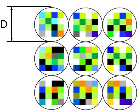
9 Features of electronic cluster eyes (ecley) Demonstrator ecley VGA d = 10 mm d = 25 mm Size comparison: VGA webcam lens vs. ecley VGA demonstrator d = 50 mm d = 250 mm focusing = correction for parallax software focusing / refocusing measured depth map multiaperture parallax -> disparity Object distance: 4m, 70 diagonal FOV DoF : Depth of field (proportional to depth of focus) 1.4mm optics z-height large DoF (4mm - ) depth imaging A. Oberdörster et. al., "Digital focusing and re-focusing with thin multi-aperture cameras", in Proc. SPIE 8299, p (2012). 9


10 Novel microlens technology opt. design recent prototypes were based on reflow of photo resist limited fill-factor, f/# and resolution standard micro lens array chirped array of ellipsoidal lenses enhance resolution need more degrees of freedom increase optical fill-factor new microlens technology: freeform microlens segment array 10

11 Novel microlens technology mastering Ultra precision diamond machining + Step&Repeat imprinting milling & planing generation of masters for single microlens arrays Step&Repeat process generation of array-masters for many MLAs on common substrate 11


. F.")
12 Novel microlens technology Fabrication process chain Data compilation & transfer Single master Imprint tool Array master Optics modul surface description alignment marks yard structures UP-machining Aluminium / NiP UV transparent polymer / epoxybased Step & Repeat multiple imprint replication Mask Aligner replication & stacking Charakterisierung tactile und interferometrical characterization pre-compensation J. Dunkel, et. al.,proc. SPIE 8763, p (2013). F. Wippermann, et. al., 18th Microoptics Conference (MOC 13), (2013). 12
![Formabweichung [nm] (rms) Fraunhofer IOF Novel microlens technology Step & Repeat replication process measured master properties surface roughness ~ 8nm (RMS) 100 90 80 70 60 50 40 30 20 10 0 8](/docs-images/85/92729629/images/13-3.jpg "master wafer with refractive freeform lenslet arrays 001-002-MS-005_chan00 001-002-MS-005_chan01 001-002-MS-005_chan02 001-002-MS-005_chan03 001-002-MS-005_chan04 001-002-MS-005_chan10")
13 Formabweichung [nm] (rms) Fraunhofer IOF Novel microlens technology Step & Repeat replication process measured master properties surface roughness ~ 8nm (RMS) master wafer with refractive freeform lenslet arrays MS-005_chan MS-005_chan MS-005_chan MS-005_chan MS-005_chan MS-005_chan MS-005_chan MS-005_chan MS-005_chan MS-005_chan MS-005_chan MS-005_chan MS-005_chan MS-005_chan MS-005_chan MS-005_chan MS-005_chan MS-005_chan MS-005_chan MS-005_chan MS-005_chan MS-005_chan MS-005_chan MS-005_chan MS-005_chan MS-005_chan MS-005_chan MS-005_chan MS-005_chan MS-005_chan MS-005_chan MS-005_chan MS-005_chan MS-005_chan MS-005_chan MS-005_chan MS-005_chan MS-005_chan MS-005_chan73 av. shape deviation ~ 52nm (RMS) MS-005_chan74 J. Dunkel, et. al.,proc. SPIE 8763, p (2013). F. Wippermann, et. al., 18th Microoptics Conference (MOC 13), (2013). 13

. F. Wippermann, et. al.")
14 Novel microlens technology Step & Repeat replication process 8 master wafer with refractive freeform lenslet arrays double-sided replicated multi-aperture objective J. Dunkel, et. al.,proc. SPIE 8763, p (2013). F. Wippermann, et. al., 18th Microoptics Conference (MOC 13), (2013). 14


15 Prototyping results Demonstrator ecley 720p customized image sensor* multi-aperture lens module camera module layout camera assembly 1.9mm optics z-height * developed by partner Fraunhofer IIS, Erlangen, fabricated by TowerJazz 15

16 Prototyping results Demonstrator ecley 720p on-axis MTF measurement preliminary camera demonstrator cutoff frequency: 300 cycles/mm Parameter diag. FOV Fno. image res. in pixels Value x 768 TTL no. of cells no. of pixels per cell FOV per cell pixel pitch sensor die size 1.9mm 15 x 9 96 x µm 6.4mm x 4.15mm fill fact or* 31% A. Brückner, et. al., "Ultra-thin wafer-level camera with 720p resolution using microoptics," Proc. SPIE 9193, (2014). 16
17 Prototyping results Characterization through focus MTF measurement scanning 100µm defocus with 5µm steps > 30% over 40µm defocus off-axis MTF measurement intermediate field at 18 AOI MTF is in good agreement with simulation AOI : Angle of incidence 17
18 Prototyping results Image reconstruction Real time image reconstruction: Image acquisition (raw data) Flat-Field Correction Distortion correction Raw image (channel-wise) Pixel redistribution (Braiding pattern & parallax correction) braiding coded into optical module by design algorithms of low complexity frame rate: 30 fps possible in mobile devices Reconstructed image A. Oberdörster, et. al., "Interactive alignment and image reconstruction for waferlevel multi-aperture camera systems," Proc. SPIE 9217, (2014). 18

19 Prototyping results Image reconstruction Raw image Reconstructed image ongoing work: optimization of image reconstruction (correction of sensor pixel characteristics) small batch series applying precompensation integration with lens housing A. Oberdörster, et. al., "Interactive alignment and image reconstruction for waferlevel multi-aperture camera systems," Proc. SPIE 9217, (2014). 19
20 Agenda Motivation Features of electronic cluster eyes Novel microlens technology Prototyping results Summary


21 Summary multi-aperture enables new freedom for miniaturized imaging systems design by fusion of micro-optics micro-electronics image processing extreme miniaturization segmentation of field-of-view reduction of costs parallelized fabrication and partly assembly on wafer level unique features for slimmer consumer products 21


22 Thank you. The presented work has been funded by: in a project of the Fraunhofer Future Foundation
Lecture Notes 10 Image Sensor Optics. Imaging optics. Pixel optics. Microlens
 Lecture Notes 10 Image Sensor Optics Imaging optics Space-invariant model Space-varying model Pixel optics Transmission Vignetting Microlens EE 392B: Image Sensor Optics 10-1 Image Sensor Optics Microlens
Compact camera module testing equipment with a conversion lens
 Compact camera module testing equipment with a conversion lens Jui-Wen Pan* 1 Institute of Photonic Systems, National Chiao Tung University, Tainan City 71150, Taiwan 2 Biomedical Electronics Translational
Using molded chalcogenide glass technology to reduce cost in a compact wide-angle thermal imaging lens
 Using molded chalcogenide glass technology to reduce cost in a compact wide-angle thermal imaging lens George Curatu a, Brent Binkley a, David Tinch a, and Costin Curatu b a LightPath Technologies, 2603
Simple telecentric submillimeter lens with near-diffraction-limited performance across an 80 degree field of view
 8752 Vol. 55, No. 31 / November 1 2016 / Applied Optics Research Article Simple telecentric submillimeter lens with near-diffraction-limited performance across an 80 degree field of view MOHSEN REZAEI,
UV EXCIMER LASER BEAM HOMOGENIZATION FOR MICROMACHINING APPLICATIONS
 Optics and Photonics Letters Vol. 4, No. 2 (2011) 75 81 c World Scientific Publishing Company DOI: 10.1142/S1793528811000226 UV EXCIMER LASER BEAM HOMOGENIZATION FOR MICROMACHINING APPLICATIONS ANDREW
PROCEEDINGS OF SPIE. Measurement of low-order aberrations with an autostigmatic microscope
 PROCEEDINGS OF SPIE SPIEDigitalLibrary.org/conference-proceedings-of-spie Measurement of low-order aberrations with an autostigmatic microscope William P. Kuhn Measurement of low-order aberrations with
Digital Photographic Imaging Using MOEMS
 Digital Photographic Imaging Using MOEMS Vasileios T. Nasis a, R. Andrew Hicks b and Timothy P. Kurzweg a a Department of Electrical and Computer Engineering, Drexel University, Philadelphia, USA b Department
The Challenge. SPOT Vegetation. miniaturization. Proba Vegetation. Technology assessment:
 The Challenge Spot-5 lifetime expires in 2012. The next French satellite, Pleiades, is solely dedicated to HiRes. The Belgian Federal Science Policy Office (BELSPO) declared their interest to develop an
Optics Manufacturing
 Optics Manufacturing SCHNEIDER product families Ophthalmics Ultra-precision optics Precision optics The Modulo system First integrated production system Basics of Cup Wheel Grinding for Spherical Lenses
Next generation IR imaging component requirements
 Next generation IR imaging component requirements Dr Andy Wood VP Technology Optical Systems November 2017 0 2013 Excelitas Technologies E N G A G E. E N A B L E. E X C E L. 0 Some background Optical design
Imaging with microlenslet arrays
 Imaging with microlenslet arrays Vesselin Shaoulov, Ricardo Martins, and Jannick Rolland CREOL / School of Optics University of Central Florida Orlando, Florida 32816 Email: vesko@odalab.ucf.edu 1. ABSTRACT
Hexagonal Liquid Crystal Micro-Lens Array with Fast-Response Time for Enhancing Depth of Light Field Microscopy
 Hexagonal Liquid Crystal Micro-Lens Array with Fast-Response Time for Enhancing Depth of Light Field Microscopy Chih-Kai Deng 1, Hsiu-An Lin 1, Po-Yuan Hsieh 2, Yi-Pai Huang 2, Cheng-Huang Kuo 1 1 2 Institute
Photolithography II ( Part 2 )
") 1 Photolithography II ( Part 2 ) Chapter 14 : Semiconductor Manufacturing Technology by M. Quirk & J. Serda Saroj Kumar Patra, Department of Electronics and Telecommunication, Norwegian University of Science
1 Photolithography II ( Part 2 ) Chapter 14 : Semiconductor Manufacturing Technology by M. Quirk & J. Serda Saroj Kumar Patra, Department of Electronics and Telecommunication, Norwegian University of Science
Compact Dual Field-of-View Telescope for Small Satellite Payloads. Jim Peterson Trent Newswander
 Compact Dual Field-of-View Telescope for Small Satellite Payloads Jim Peterson Trent Newswander Introduction & Overview Small satellite payloads with multiple FOVs commonly sought Wide FOV to search or
Figure 7 Dynamic range expansion of Shack- Hartmann sensor using a spatial-light modulator
 Figure 4 Advantage of having smaller focal spot on CCD with super-fine pixels: Larger focal point compromises the sensitivity, spatial resolution, and accuracy. Figure 1 Typical microlens array for Shack-Hartmann
Miniaturization trends in medical imaging enabled by full wafer level integration if micro camera modules
 Miniaturization trends in medical imaging enabled by full wafer level integration if micro camera modules About AWAIBA o Excellence in Custom design & Standard Sensor components for Medical imaging and
WaveMaster IOL. Fast and Accurate Intraocular Lens Tester
 WaveMaster IOL Fast and Accurate Intraocular Lens Tester INTRAOCULAR LENS TESTER WaveMaster IOL Fast and accurate intraocular lens tester WaveMaster IOL is an instrument providing real time analysis of
Innovative Mask Aligner Lithography for MEMS and Packaging
 Innovative Mask Aligner Lithography for MEMS and Packaging Dr. Reinhard Voelkel CEO SUSS MicroOptics SA September 9 th, 2010 1 SUSS Micro-Optics SUSS MicroOptics is a leading supplier for high-quality
WaveMaster IOL. Fast and accurate intraocular lens tester
 WaveMaster IOL Fast and accurate intraocular lens tester INTRAOCULAR LENS TESTER WaveMaster IOL Fast and accurate intraocular lens tester WaveMaster IOL is a new instrument providing real time analysis
Use of Computer Generated Holograms for Testing Aspheric Optics
 Use of Computer Generated Holograms for Testing Aspheric Optics James H. Burge and James C. Wyant Optical Sciences Center, University of Arizona, Tucson, AZ 85721 http://www.optics.arizona.edu/jcwyant,
Integrated Multi-Aperture Imaging
 Integrated Multi-Aperture Imaging Keith Fife, Abbas El Gamal, Philip Wong Department of Electrical Engineering, Stanford University, Stanford, CA 94305 1 Camera History 2 Camera History Despite progress,
Parallel Mode Confocal System for Wafer Bump Inspection
 Parallel Mode Confocal System for Wafer Bump Inspection ECEN5616 Class Project 1 Gao Wenliang wen-liang_gao@agilent.com 1. Introduction In this paper, A parallel-mode High-speed Line-scanning confocal
Wavefront sensing by an aperiodic diffractive microlens array
 Wavefront sensing by an aperiodic diffractive microlens array Lars Seifert a, Thomas Ruppel, Tobias Haist, and Wolfgang Osten a Institut für Technische Optik, Universität Stuttgart, Pfaffenwaldring 9,
Hochperformante Inline-3D-Messung
 Hochperformante Inline-3D-Messung mittels Lichtfeld Dipl.-Ing. Dorothea Heiss Deputy Head of Business Unit High Performance Image Processing Digital Safety & Security Department AIT Austrian Institute
Synopsis of paper. Optomechanical design of multiscale gigapixel digital camera. Hui S. Son, Adam Johnson, et val.
 Synopsis of paper --Xuan Wang Paper title: Author: Optomechanical design of multiscale gigapixel digital camera Hui S. Son, Adam Johnson, et val. 1. Introduction In traditional single aperture imaging
Development of a new multi-wavelength confocal surface profilometer for in-situ automatic optical inspection (AOI)
") Development of a new multi-wavelength confocal surface profilometer for in-situ automatic optical inspection (AOI) Liang-Chia Chen 1#, Chao-Nan Chen 1 and Yi-Wei Chang 1 1. Institute of Automation Technology,
Development of a new multi-wavelength confocal surface profilometer for in-situ automatic optical inspection (AOI) Liang-Chia Chen 1#, Chao-Nan Chen 1 and Yi-Wei Chang 1 1. Institute of Automation Technology,
Potential benefits of freeform optics for the ELT instruments. J. Kosmalski
 Potential benefits of freeform optics for the ELT instruments J. Kosmalski Freeform Days, 12-13 th October 2017 Summary Introduction to E-ELT intruments Freeform design for MAORY LGS Free form design for
TECHSPEC COMPACT FIXED FOCAL LENGTH LENS
 Designed for use in machine vision applications, our TECHSPEC Compact Fixed Focal Length Lenses are ideal for use in factory automation, inspection or qualification. These machine vision lenses have been
Copyright 2005 Society of Photo Instrumentation Engineers.
 Copyright 2005 Society of Photo Instrumentation Engineers. This paper was published in SPIE Proceedings, Volume 5874 and is made available as an electronic reprint with permission of SPIE. One print or
Improving techniques for Shack-Hartmann wavefront sensing: dynamic-range and frame rate
 Improving techniques for Shack-Hartmann wavefront sensing: dynamic-range and frame rate Takao Endo, Yoshichika Miwa, Jiro Suzuki and Toshiyuki Ando Information Technology R&D Center, Mitsubishi Electric
Compact Dual Field-of-View Telescope for Small Satellite Payloads
 Compact Dual Field-of-View Telescope for Small Satellite Payloads James C. Peterson Space Dynamics Laboratory 1695 North Research Park Way, North Logan, UT 84341; 435-797-4624 Jim.Peterson@sdl.usu.edu
CODE V Introductory Tutorial
 CODE V Introductory Tutorial Cheng-Fang Ho Lab.of RF-MW Photonics, Department of Physics, National Cheng-Kung University, Tainan, Taiwan 1-1 Tutorial Outline Introduction to CODE V Optical Design Process
Micro- and Nano-Technology... for Optics
 Micro- and Nano-Technology...... for Optics 3.2 Lithography U.D. Zeitner Fraunhofer Institut für Angewandte Optik und Feinmechanik Jena Printing on Stones Map of Munich Stone Print Contact Printing light
Difrotec Product & Services. Ultra high accuracy interferometry & custom optical solutions
 Difrotec Product & Services Ultra high accuracy interferometry & custom optical solutions Content 1. Overview 2. Interferometer D7 3. Benefits 4. Measurements 5. Specifications 6. Applications 7. Cases
Microlens array-based exit pupil expander for full color display applications
 Proc. SPIE, Vol. 5456, in Photon Management, Strasbourg, France, April 2004 Microlens array-based exit pupil expander for full color display applications Hakan Urey a, Karlton D. Powell b a Optical Microsystems
Vision Research at. Validation of a Novel Hartmann-Moiré Wavefront Sensor with Large Dynamic Range. Wavefront Science Congress, Feb.
 Wavefront Science Congress, Feb. 2008 Validation of a Novel Hartmann-Moiré Wavefront Sensor with Large Dynamic Range Xin Wei 1, Tony Van Heugten 2, Nikole L. Himebaugh 1, Pete S. Kollbaum 1, Mei Zhang
Developments, Applications and Challenges for the Industrial Implementation of Nanoimprint Lithography
 Developments, Applications and Challenges for the Industrial Implementation of Nanoimprint Lithography Martin Eibelhuber, Business Development Manager m.eibelhuber@evgroup.com Outline Introduction Imprint
Fabrication Methodology of microlenses for stereoscopic imagers using standard CMOS process. R. P. Rocha, J. P. Carmo, and J. H.
 Fabrication Methodology of microlenses for stereoscopic imagers using standard CMOS process R. P. Rocha, J. P. Carmo, and J. H. Correia Department of Industrial Electronics, University of Minho, Campus
IMAGE SENSOR SOLUTIONS. KAC-96-1/5" Lens Kit. KODAK KAC-96-1/5" Lens Kit. for use with the KODAK CMOS Image Sensors. November 2004 Revision 2
 KODAK for use with the KODAK CMOS Image Sensors November 2004 Revision 2 1.1 Introduction Choosing the right lens is a critical aspect of designing an imaging system. Typically the trade off between image
LIQUID CRYSTAL LENSES FOR CORRECTION OF P ~S~YOP
 LIQUID CRYSTAL LENSES FOR CORRECTION OF P ~S~YOP GUOQIANG LI and N. PEYGHAMBARIAN College of Optical Sciences, University of Arizona, Tucson, A2 85721, USA Email: gli@ootics.arizt~ii~.e~i~ Correction of
Lithography. 3 rd. lecture: introduction. Prof. Yosi Shacham-Diamand. Fall 2004
 Lithography 3 rd lecture: introduction Prof. Yosi Shacham-Diamand Fall 2004 1 List of content Fundamental principles Characteristics parameters Exposure systems 2 Fundamental principles Aerial Image Exposure
EE-527: MicroFabrication
 EE-57: MicroFabrication Exposure and Imaging Photons white light Hg arc lamp filtered Hg arc lamp excimer laser x-rays from synchrotron Electrons Ions Exposure Sources focused electron beam direct write
Ron Liu OPTI521-Introductory Optomechanical Engineering December 7, 2009
 Synopsis of METHOD AND APPARATUS FOR IMPROVING VISION AND THE RESOLUTION OF RETINAL IMAGES by David R. Williams and Junzhong Liang from the US Patent Number: 5,777,719 issued in July 7, 1998 Ron Liu OPTI521-Introductory
Design and optimization of microlens array based high resolution beam steering system
 Design and optimization of microlens array based high resolution beam steering system Ata Akatay and Hakan Urey Department of Electrical Engineering, Koc University, Sariyer, Istanbul 34450, Turkey hurey@ku.edu.tr
Mask projection surface structuring
 Willkommen Welcome Bienvenue Mask projection surface structuring Patrik Hoffmann Advanced Materials Processing Empa Thun, Switzerland EPHJ - Geneva, 18.6.2014 Outline Ablation process - limitations Excimer
Lecture 22 Optical MEMS (4)
") EEL6935 Advanced MEMS (Spring 2005) Instructor: Dr. Huikai Xie Lecture 22 Optical MEMS (4) Agenda: Refractive Optical Elements Microlenses GRIN Lenses Microprisms Reference: S. Sinzinger and J. Jahns,
EEL6935 Advanced MEMS (Spring 2005) Instructor: Dr. Huikai Xie Lecture 22 Optical MEMS (4) Agenda: Refractive Optical Elements Microlenses GRIN Lenses Microprisms Reference: S. Sinzinger and J. Jahns,
DETERMINING CALIBRATION PARAMETERS FOR A HARTMANN- SHACK WAVEFRONT SENSOR
 DETERMINING CALIBRATION PARAMETERS FOR A HARTMANN- SHACK WAVEFRONT SENSOR Felipe Tayer Amaral¹, Luciana P. Salles 2 and Davies William de Lima Monteiro 3,2 Graduate Program in Electrical Engineering -
PolarCam and Advanced Applications
 PolarCam and Advanced Applications Workshop Series 2013 Outline Polarimetry Background Stokes vector Types of Polarimeters Micro-polarizer Camera Data Processing Application Examples Passive Illumination
Building a Real Camera
 Building a Real Camera Home-made pinhole camera Slide by A. Efros http://www.debevec.org/pinhole/ Shrinking the aperture Why not make the aperture as small as possible? Less light gets through Diffraction
12.4 Alignment and Manufacturing Tolerances for Segmented Telescopes
 330 Chapter 12 12.4 Alignment and Manufacturing Tolerances for Segmented Telescopes Similar to the JWST, the next-generation large-aperture space telescope for optical and UV astronomy has a segmented
Compact ellipsometer employing a static polarimeter module with arrayed polarizer and wave-plate elements
 Compact ellipsometer employing a static polarimeter module with arrayed polarizer and wave-plate elements Takashi Sato, 1 Takeshi Araki, 1 Yoshihiro Sasaki, 2 Toshihide Tsuru, 3 Toshiyasu Tadokoro, 1 and
Standards for microlenses and microlens arrays
 Digital Futures 2008 Institute of Physics, London 28 October 2008 Standards for microlenses and microlens arrays Richard Stevens Quality of Life Division, National Physical Laboratory, Teddington, TW11
Pulsed Laser Ablation of Polymers for Display Applications
 Pulsed Laser Ablation of Polymers for Display Applications James E.A Pedder 1, Andrew S. Holmes 2, Heather J. Booth 1 1 Oerlikon Optics UK Ltd, Oxford Industrial Estate, Yarnton, Oxford, OX5 1QU, UK 2
Applying of refractive beam shapers of circular symmetry to generate non-circular shapes of homogenized laser beams
 - 1 - Applying of refractive beam shapers of circular symmetry to generate non-circular shapes of homogenized laser beams Alexander Laskin a, Vadim Laskin b a MolTech GmbH, Rudower Chaussee 29-31, 12489
PicoMaster 100. Unprecedented finesse in creating 3D micro structures. UV direct laser writer for maskless lithography
 UV direct laser writer for maskless lithography Unprecedented finesse in creating 3D micro structures Highest resolution in the market utilizing a 405 nm diode laser Structures as small as 300 nm 375 nm
Lecture 18: Light field cameras. (plenoptic cameras) Visual Computing Systems CMU , Fall 2013
 Visual Computing Systems CMU , Fall 2013") Lecture 18: Light field cameras (plenoptic cameras) Visual Computing Systems Continuing theme: computational photography Cameras capture light, then extensive processing produces the desired image Today:
Lecture 18: Light field cameras (plenoptic cameras) Visual Computing Systems Continuing theme: computational photography Cameras capture light, then extensive processing produces the desired image Today:
CXCI. Optical design of a compact telescope for the next generation Earth Observation system CXCI. Vincent COSTES. Octobre 2012
 CXCI Optical design of a compact telescope for the next generation Earth Observation system Vincent COSTES Octobre 2012 CXCI CXCI SUMMARY INTRODUCTION CXCI TECHNOLOGICAL PROGRAM COMPACTNESS REQUIREMENT
PROJECT. DOCUMENT IDENTIFICATION D2.2 - Report on low cost filter deposition process DISSEMINATION STATUS PUBLIC DUE DATE 30/09/2011 ISSUE 2 PAGES 16
 GRANT AGREEMENT NO. ACRONYM TITLE CALL FUNDING SCHEME 248898 PROJECT 2WIDE_SENSE WIDE spectral band & WIDE dynamics multifunctional imaging SENSor ENABLING SAFER CAR TRANSPORTATION FP7-ICT-2009.6.1 STREP
Beam deflection technologies for ultra short pulse lasers June 5th, 2018
 Beam deflection technologies for ultra short pulse lasers June 5th, 2018 Agenda SCANLAB GmbH XL Scan excellishift precsys 2 SCANLAB at a Glance Worldwide leading OEM manufacturer of scan solutions for
MICROMACHINED INTERFEROMETER FOR MEMS METROLOGY
 MICROMACHINED INTERFEROMETER FOR MEMS METROLOGY Byungki Kim, H. Ali Razavi, F. Levent Degertekin, Thomas R. Kurfess G.W. Woodruff School of Mechanical Engineering, Georgia Institute of Technology, Atlanta,
The manuscript is clearly written and the results are well presented. The results appear to be valid and the methodology is appropriate.
 Reviewers' comments: Reviewer #1 (Remarks to the Author): The manuscript titled An optical metasurface planar camera by Arbabi et al, details theoretical and experimental investigations into the development
Adaptive Optics for LIGO
 Adaptive Optics for LIGO Justin Mansell Ginzton Laboratory LIGO-G990022-39-M Motivation Wavefront Sensor Outline Characterization Enhancements Modeling Projections Adaptive Optics Results Effects of Thermal
To Do. Advanced Computer Graphics. Outline. Computational Imaging. How do we see the world? Pinhole camera
 Advanced Computer Graphics CSE 163 [Spring 2017], Lecture 14 Ravi Ramamoorthi http://www.cs.ucsd.edu/~ravir To Do Assignment 2 due May 19 Any last minute issues or questions? Next two lectures: Imaging,
BMC s heritage deformable mirror technology that uses hysteresis free electrostatic
 Optical Modulator Technical Whitepaper MEMS Optical Modulator Technology Overview The BMC MEMS Optical Modulator, shown in Figure 1, was designed for use in free space optical communication systems. The
Conformal optical system design with a single fixed conic corrector
 Conformal optical system design with a single fixed conic corrector Song Da-Lin( ), Chang Jun( ), Wang Qing-Feng( ), He Wu-Bin( ), and Cao Jiao( ) School of Optoelectronics, Beijing Institute of Technology,
Testing Aspheric Lenses: New Approaches
 Nasrin Ghanbari OPTI 521 - Synopsis of a published Paper November 5, 2012 Testing Aspheric Lenses: New Approaches by W. Osten, B. D orband, E. Garbusi, Ch. Pruss, and L. Seifert Published in 2010 Introduction
Variable microinspection system. system125
 Variable microinspection system system125 Variable micro-inspection system Characteristics Large fields, high NA The variable microinspection system mag.x system125 stands out from conventional LD inspection
Refractive index homogeneity TWE effect on large aperture optical systems
 Refractive index homogeneity TWE effect on large aperture optical systems M. Stout*, B. Neff II-VI Optical Systems 36570 Briggs Road., Murrieta, CA 92563 ABSTRACT Sapphire windows are routinely being used
e2v Launches New Onyx 1.3M for Premium Performance in Low Light Conditions
 e2v Launches New Onyx 1.3M for Premium Performance in Low Light Conditions e2v s Onyx family of image sensors is designed for the most demanding outdoor camera and industrial machine vision applications,
Wavelength Stabilization of HPDL Array Fast-Axis Collimation Optic with integrated VHG
 Wavelength Stabilization of HPDL Array Fast-Axis Collimation Optic with integrated VHG C. Schnitzler a, S. Hambuecker a, O. Ruebenach a, V. Sinhoff a, G. Steckman b, L. West b, C. Wessling c, D. Hoffmann
Radial Coupling Method for Orthogonal Concentration within Planar Micro-Optic Solar Collectors
 Radial Coupling Method for Orthogonal Concentration within Planar Micro-Optic Solar Collectors Jason H. Karp, Eric J. Tremblay and Joseph E. Ford Photonics Systems Integration Lab University of California
Low speckle laser illuminated projection system with a vibrating diffractive beam shaper
 Low speckle laser illuminated projection system with a vibrating diffractive beam shaper Po-Hung Yao, Chieh-Hui Chen, and Cheng-Huan Chen* Department of Power Mechanical Engineering, National TsingHua
Three-dimensional quantitative phase measurement by Commonpath Digital Holographic Microscopy
 Available online at www.sciencedirect.com Physics Procedia 19 (2011) 291 295 International Conference on Optics in Precision Engineering and Nanotechnology Three-dimensional quantitative phase measurement
Multiple-Field Approach for Aberration Correction in Miniature Imaging Systems Based on Wafer-Level Production
 Multiple-Field Approach for Aberration Correction in Miniature Imaging Systems Based on Wafer-Level Production Eric Logean a, Toralf Scharf a, Nicolas Bongard a, Hans Peter Herzig a, Markus Rossi b a Optics
DIMENSIONAL MEASUREMENT OF MICRO LENS ARRAY WITH 3D PROFILOMETRY
 DIMENSIONAL MEASUREMENT OF MICRO LENS ARRAY WITH 3D PROFILOMETRY Prepared by Benjamin Mell 6 Morgan, Ste156, Irvine CA 92618 P: 949.461.9292 F: 949.461.9232 nanovea.com Today's standard for tomorrow's
7x P/N C1601. General Description
 METRICZOOM SWIR 7x METRIC ZOOM-SWIR ZOOM 7x P/N C1601 C General Description This family of high resolution METRIC ZOOM SWIR lenses image from 0.9 to 2.3 µm making them especially well-suited well for surveillance,
EUVL Activities in China. Xiangzhao Wang Shanghai Inst. Of Opt. and Fine Mech. Of CAS. (SIOM) Shanghai, China.
 Shanghai, China.") EUVL Activities in China Xiangzhao Wang Shanghai Inst. Of Opt. and Fine Mech. Of CAS. (SIOM) Shanghai, China. wxz26267@siom.ac.cn Projection Optics Imaging System Surface Testing Optical Machining ML Coating
EUVL Activities in China Xiangzhao Wang Shanghai Inst. Of Opt. and Fine Mech. Of CAS. (SIOM) Shanghai, China. wxz26267@siom.ac.cn Projection Optics Imaging System Surface Testing Optical Machining ML Coating
Camera Calibration Certificate No: DMC II
 Calibration DMC II 230 027 Camera Calibration Certificate No: DMC II 230 027 For Peregrine Aerial Surveys, Inc. 103-20200 56 th Ave Langley, BC V3A 8S1 Canada Calib_DMCII230-027.docx Document Version 3.0
Integrated Focusing Photoresist Microlenses on AlGaAs Top-Emitting VCSELs
 Integrated Focusing Photoresist Microlenses on AlGaAs Top-Emitting VCSELs Andrea Kroner We present 85 nm wavelength top-emitting vertical-cavity surface-emitting lasers (VCSELs) with integrated photoresist
Factors Affecting Pixel Scaling Limits for cellphone imaging systems
 Factors Affecting Pixel Scaling Limits for cellphone imaging systems October 28, 2010 Richard Crisp rcrisp@narrowbandimaging.com Agenda Pixel Scaling Limits Optical Considerations Image Sensor Considerations
Strategies for low cost imprint molds
 Strategies for low cost imprint molds M.P.C. Watts, Impattern Solutions, 9404 Bell Mountain Drive Austin TX 78730 www.impattern.com ABSTRACT The Cost of ownership (COO) due to the mold can be minimized
Novel Hemispheric Image Formation: Concepts & Applications
 Novel Hemispheric Image Formation: Concepts & Applications Simon Thibault, Pierre Konen, Patrice Roulet, and Mathieu Villegas ImmerVision 2020 University St., Montreal, Canada H3A 2A5 ABSTRACT Panoramic
Feature-level Compensation & Control
 Feature-level Compensation & Control 2 Sensors and Control Nathan Cheung, Kameshwar Poolla, Costas Spanos Workshop 11/19/2003 3 Metrology, Control, and Integration Nathan Cheung, UCB SOI Wafers Multi wavelength
(12) Patent Application Publication (10) Pub. No.: US 2007/ A1
 Patent Application Publication (10) Pub. No.: US 2007/ A1") (19) United States (12) Patent Application Publication (10) Pub. No.: US 2007/0132875 A1 Lee et al. US 20070132875A1 (43) Pub. Date: Jun. 14, 2007 (54) (75) (73) (21) (22) (30) OPTICAL LENS SYSTEM OF MOBILE
(19) United States (12) Patent Application Publication (10) Pub. No.: US 2007/0132875 A1 Lee et al. US 20070132875A1 (43) Pub. Date: Jun. 14, 2007 (54) (75) (73) (21) (22) (30) OPTICAL LENS SYSTEM OF MOBILE
Study of self-interference incoherent digital holography for the application of retinal imaging
 Study of self-interference incoherent digital holography for the application of retinal imaging Jisoo Hong and Myung K. Kim Department of Physics, University of South Florida, Tampa, FL, US 33620 ABSTRACT
Proposed Adaptive Optics system for Vainu Bappu Telescope
 Proposed Adaptive Optics system for Vainu Bappu Telescope Essential requirements of an adaptive optics system Adaptive Optics is a real time wave front error measurement and correction system The essential
LENSES. INEL 6088 Computer Vision
 LENSES INEL 6088 Computer Vision Digital camera A digital camera replaces film with a sensor array Each cell in the array is a Charge Coupled Device light-sensitive diode that converts photons to electrons
Optical Characterization and Defect Inspection for 3D Stacked IC Technology
 Minapad 2014, May 21 22th, Grenoble; France Optical Characterization and Defect Inspection for 3D Stacked IC Technology J.Ph.Piel, G.Fresquet, S.Perrot, Y.Randle, D.Lebellego, S.Petitgrand, G.Ribette FOGALE
doi: /
 doi: 10.1117/12.872287 Coarse Integral Volumetric Imaging with Flat Screen and Wide Viewing Angle Shimpei Sawada* and Hideki Kakeya University of Tsukuba 1-1-1 Tennoudai, Tsukuba 305-8573, JAPAN ABSTRACT
MICRO AND NANOPROCESSING TECHNOLOGIES
 MICRO AND NANOPROCESSING TECHNOLOGIES LECTURE 4 Optical lithography Concepts and processes Lithography systems Fundamental limitations and other issues Photoresists Photolithography process Process parameter
How to Choose a Machine Vision Camera for Your Application.
 Vision Systems Design Webinar 9 September 2015 How to Choose a Machine Vision Camera for Your Application. Andrew Bodkin Bodkin Design & Engineering, LLC Newton, MA 02464 617-795-1968 wab@bodkindesign.com
Aberrations and adaptive optics for biomedical microscopes
 Aberrations and adaptive optics for biomedical microscopes Martin Booth Department of Engineering Science And Centre for Neural Circuits and Behaviour University of Oxford Outline Rays, wave fronts and
Building a Real Camera. Slides Credit: Svetlana Lazebnik
 Building a Real Camera Slides Credit: Svetlana Lazebnik Home-made pinhole camera Slide by A. Efros http://www.debevec.org/pinhole/ Shrinking the aperture Why not make the aperture as small as possible?
Carl Zeiss SMT. ACTOP 2008: Presentation Carl Zeiss Laser Optics. H. Thiess. LO-GOO Oct. 9, 2008
 Carl Zeiss SMT ACTOP 2008: Presentation Carl Zeiss Laser Optics H. Thiess LO-GOO Oct. 9, 2008 for public use Seite 1 Outline! Zeiss has decades of experience as optics manufacturer. Dedication to mirror
Optical and mechanical parameters. 100 mm N. of elements 20.5 mm Dimensions 11.7 degrees Weight F/N = 4 (fixed) N.A.
 N.A.") OB SWIR 100 LENS OB-SWIR100/4 P/N C0416 General Description This family of high resolution SWIR lenses image from 0.9 2.3 µmm making them especially well-suited for PCB inspection, special laser applications,
OB SWIR 100 LENS OB-SWIR100/4 P/N C0416 General Description This family of high resolution SWIR lenses image from 0.9 2.3 µmm making them especially well-suited for PCB inspection, special laser applications,
Spatially Resolved Backscatter Ceilometer
 Spatially Resolved Backscatter Ceilometer Design Team Hiba Fareed, Nicholas Paradiso, Evan Perillo, Michael Tahan Design Advisor Prof. Gregory Kowalski Sponsor, Spectral Sciences Inc. Steve Richstmeier,
Diffraction, Fourier Optics and Imaging
 1 Diffraction, Fourier Optics and Imaging 1.1 INTRODUCTION When wave fields pass through obstacles, their behavior cannot be simply described in terms of rays. For example, when a plane wave passes through
Half-tone proximity lithography
 Half-tone proximity lithography Torsten Harzendorf* a, Lorenz Stuerzebecher a, Uwe Vogler b, Uwe D. Zeitner a, Reinhard Voelkel b a Fraunhofer Institut für Angewandte Optik und Feinmechanik IOF, Albert
German Photonics Industry - Products & Innovations SPIE Photonics West Exhibition, 5-7 February 2013
 Laser Technology, Research and Development Contact person for the media Steffen Böhme Tapering of different optical components with CO 2-laser Laser based tapering overcomes typical limitations of conventional
Tech Paper. Anti-Sparkle Film Distinctness of Image Characterization
 Tech Paper Anti-Sparkle Film Distinctness of Image Characterization Anti-Sparkle Film Distinctness of Image Characterization Brian Hayden, Paul Weindorf Visteon Corporation, Michigan, USA Abstract: The