Akiyama-Probe (A-Probe) guide
|
|
|
- Bonnie Carpenter
- 5 years ago
- Views:
Transcription
1 Akiyama-Probe (A-Probe) guide This guide presents: what is Akiyama-Probe, how it works, and its performance. Akiyama-Probe is a patented technology. Version:

2 Introduction NANOSENSORS Akiyama-Probe (A-Probe) is a novel self-sensing and self-actuating (-exciting) probe based on a quartz tuning fork combined with a micromachined cantilever for dynamic mode AFM. The great advantage of this novel probe is that one can benefit from both the tuning fork's extremely stable oscillation and the silicon cantilever's reasonable spring constant with one probe. Akiyama-Probe is equipped with a high-end sharp silicon tip and has an excellent imaging capability on various samples with different properties, which is as high as a conventional optical lever system. Akiyama-Probe requires neither optical detection, nor external shaker. Akiyama-Probe occupies only a small space above the sample. These features make it very attractive for creating new generation SPM instruments.


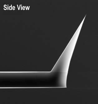
 AdvancedTEC -like tip radius <15 nm, tip height 28 µm 5 N/m (Si")
3 Akiyama-Probe specifications ~ 3 mm w l The cantilever is electrically connected to one of the electrodes of the TF. Specifications (typical values) Cantilever Tip Force constant Resonance frequency Ceramic plate length: 310 µm, thickness: 3.7 µm, width: 30 µm each material: n + silicon ( Ohm cm) AdvancedTEC -like tip radius <15 nm, tip height 28 µm 5 N/m (Si cantilever) ~ 50 khz approximately 6.5 mm x 5.1 mm x 0.4 mm All values are subject to change without notice.

4 Working principle (1) In-plane movement transformed Out-of-plane motion (tip vibration) In operation, the electrical driving signal is directly applied to the electrodes of the tuning fork (TF) to excite it at its lowest resonance. In this mode, the ends of the two prongs are moving in-plane and have opposite phases, meaning that they approach and withdraw from each other. The vibration amplitude is typically in the order of tens of nm. This motion applies a small vibration at the glued ends of the cantilever, which always contains a component in z-direction (i.e., the axis of the tip) due to the twisting motion of the prongs (i.e., the cantilever disturbs a symmetry of the TF). The cantilever amplifies the vibration according to its mechanical property and a large out-ofplane motion of the tip is obtained.
5 Working principle (2) The TF is used as an oscillatory force sensor similarly to a quartz microbalance. Its frequency and amplitude are influenced by those of the tip motion. Consequently, the tip-sample interaction can be electrically detected with the TF. The recommended operation mode for Akiyama-Probe is dynamic mode with the frequency modulation (FM) detection, where the TF is self-excited (oscillating) at its first resonance frequency. During sample imaging, the resonance frequency is tracked by a phase locked loop (PLL) and kept at a set value by adjusting the tip-sample distance with a feedback loop. Selfoscillation f 0 f 1 TF influence Dynamic mode AFM The amplitude modulation (AM) detection (fixed driving frequency) is also feasible, if one would accept a slower scan speed and compromise on spatial resolution. Akiyama-Probe is designed for operation in ambient conditions. It may work in other conditions, like vacuum, UHV, or low temperatures, etc.
6 Working principle (3) k2 c2 Resonance of TF before cantilever was glued khz 1st resonance 2nd resonance m2 F k1 m1 c1 Optical detection of tip vibration Electrical signal from TF Main peak Frequency Sub peak Akiyama-Probe is a system with two coupled resonators that are moderately matched in terms of resonance frequency. The left figure illustrates a simplified model of Akiyama- Probe, where the cantilever corresponds to Resonator 1 (m1, k1, c1) and the TF to Resonator 2 (m2, k2, c2). F is the driving force created by the piezoelectric effect of the TF. Like with other similar systems, one obtains two typical resonances: in-phase (1st) and antiphase (2nd) peaks. By sweeping the driving frequency, the two large vibration peaks can be observed at the tip by optical means. In the electrical signal from the TF, one observes a large peak at the 1st resonance and a small, or almost none, peak at the 2nd resonance. The large peak at the 1st resonance is the operation frequency of Akiyama-Probe.

7 Approach curve Tip in contact, but TF is still oscillating Resonance Frequency Δf B Periodic contact A Tip oscillating in free space The figure shows a typical approach curve of Akiyama- Probe. The dashed line A indicates the critical point where the tip starts periodic contact on the sample surface. Beyond this point, the resonance frequency increases almost linearly as the tip is moved closer to the sample surface in the periodic contact region. Oscillation amplitude of the tip decreases linearly and the center of the vibration is shifted in this region (i.e., illustration at the bottom of the figure). Tip oscillation (optical observation) ΔZ The end of the periodic contact region is indicated by the dashed line B. Beyond this point, the probe works in a quasi contact mode, i.e., the tip remains in contact with the surface during the full oscillation cycle, whereas the cantilever is still vibrated by the TF. The maximum frequency shift obtained in the periodic contact region (denoted as Δf) is a specific and constant value for each probe. The distance ΔZ is about a half of the peak-to-peak amplitude of the tip oscillation in free space.


8 Approach curves One of the important features of Akiyama-Probe is that the maximum frequency shift Δf does not depend on the tip vibration amplitude. The figure shows three approach curves with different amplitude settings. It demonstrates Δf a = Δf b = Δf c. Δf a 1040 nm The sensitivity defined as the maximum frequency shift divided by the amount of tip displacement in the periodic contact region differs for each setting of the tip vibration amplitude. The sensitivity is increased as the tip vibration amplitude is decreased. Δf b 560 nm The range of Δf is approximately 30 Hz ~ 400 Hz. This is not guaranteed and subject to change without notice. Δf varies depending on temperature and humidity. Δf c 240 nm 80 nm/div

9 Long range approach curve Tip in contact, but TF is still oscillating Periodic contact Tip oscillating in free space Frequency shift Δf 13.3 µm Z position The figure shows a long range approach curve. The resonance frequency of the TF decreases gradually in the region of the quasi static mode. This region lies over a couple of tens µm in z-direction. Although Akiyama-Probe operated in this mode could be used for e.g. measuring displacement, the tip is strongly pushed onto the sample surface and, hence, operation in this mode is not recommended for AFM imaging.
10 Applications AFM imaging (topography, roughness) Measurement inside of channel Displacement measurement Light Combination with SEM/ optical microscope Multi-probe AFM imaging of light sensitive samples
 Carbon")
 Samples")


11 AFM images with Akiyama-Probe IC chip (40 µm x 40 µm) Carbon nanotube (5 µm x 5 µm) PS/PMMA film (5 µm x 5 µm) Samples from Nanosurf AG. Akiyama-Probe vs. Optical lever Akiyama-Probe µm Std. 40 N/m Si lever Tapping mode on Veeco Nanoscope III, with Nanosurf easypll, by IMT Univ. of Neuchâtel Switzerland µm

12 Akiyama-Probe in SEM EMPA Switzerland Dr. Vinzenz Friedli, Focused electron- and ion-beam induced processes : in situ monitoring, analysis and modeling, disseration EPFL, no 4036 (2008).


13 AFM images Carbon nanotube Staphylococcus aureus bacteria Atomic steps on PbSnSe etch pits Topographic images taken under ambient conditions in intermittent contact mode using Akiyama-Probe with Nanosurf Nanite A100 A-Probe AFM


14 AFM image Plasmid-DNA (2,686 bp) Scan Size : 1x1 µm Topographic images taken under ambient conditions in intermittent contact mode using Akiyama-Probe with : SXM Standard (Research Institute of Biomolecule Metrology Co., Ltd., Japan)
15 THANK YOU FOR YOUR INTEREST


16 NANOSENSORS NANOSENSORS Rue Jaquet Droz 1 Case Postale 216 CH-2002 Neuchâtel Switzerland phone: fax: info@nanosensors.com NANOSENSORS is a trademark of NanoWorld AG - Copyright by NanoWorld AG
Akiyama-Probe (A-Probe) guide
 guide") Akiyama-Probe (A-Probe) guide This guide presents: what is Akiyama-Probe, how it works, and what you can do Dynamic mode AFM Version: 2.0 Introduction NANOSENSORS Akiyama-Probe (A-Probe) is a self-sensing
Akiyama-Probe (A-Probe) guide This guide presents: what is Akiyama-Probe, how it works, and what you can do Dynamic mode AFM Version: 2.0 Introduction NANOSENSORS Akiyama-Probe (A-Probe) is a self-sensing
Akiyama-Probe (A-Probe) technical guide This technical guide presents: how to make a proper setup for operation of Akiyama-Probe.
 technical guide This technical guide presents: how to make a proper setup for operation of Akiyama-Probe.") Akiyama-Probe (A-Probe) technical guide This technical guide presents: how to make a proper setup for operation of Akiyama-Probe. Version: 2.0 Introduction To benefit from the advantages of Akiyama-Probe,
Akiyama-Probe (A-Probe) technical guide This technical guide presents: how to make a proper setup for operation of Akiyama-Probe. Version: 2.0 Introduction To benefit from the advantages of Akiyama-Probe,
Akiyama-Probe (A-Probe) simple DIY controller This technical guide presents: simple and low-budget DIY controller
 simple DIY controller This technical guide presents: simple and low-budget DIY controller") Akiyama-Probe (A-Probe) simple DIY controller This technical guide presents: simple and low-budget DIY controller Version: 2.0 Introduction NANOSENSORS has developed a simple and low-budget controller
Akiyama-Probe (A-Probe) simple DIY controller This technical guide presents: simple and low-budget DIY controller Version: 2.0 Introduction NANOSENSORS has developed a simple and low-budget controller
easypll UHV Preamplifier Reference Manual
 easypll UHV Preamplifier Reference Manual 1 Table of Contents easypll UHV-Pre-Amplifier for Tuning Fork 2 Theory... 2 Wiring of the pre-amplifier... 4 Technical specifications... 5 Version 1.1 BT 00536
- Near Field Scanning Optical Microscopy - Electrostatic Force Microscopy - Magnetic Force Microscopy
 - Near Field Scanning Optical Microscopy - Electrostatic Force Microscopy - Magnetic Force Microscopy Yongho Seo Near-field Photonics Group Leader Wonho Jhe Director School of Physics and Center for Near-field
Nanosurf Nanite. Automated AFM for Industry & Research.
 Nanosurf Nanite Automated AFM for Industry & Research www.nanosurf.com Multiple Measurements Automated Got work? Nanosurf has the solution! The Swiss-based innovator and manufacturer of the most compact
Advanced Nanoscale Metrology with AFM
 Advanced Nanoscale Metrology with AFM Sang-il Park Corp. SPM: the Key to the Nano World Initiated by the invention of STM in 1982. By G. Binnig, H. Rohrer, Ch. Gerber at IBM Zürich. Expanded by the invention
Outline: Introduction: What is SPM, history STM AFM Image treatment Advanced SPM techniques Applications in semiconductor research and industry
 1 Outline: Introduction: What is SPM, history STM AFM Image treatment Advanced SPM techniques Applications in semiconductor research and industry 2 Back to our solutions: The main problem: How to get nm
Basic methods in imaging of micro and nano structures with atomic force microscopy (AFM)
") Basic methods in imaging of micro and nano P2538000 AFM Theory The basic principle of AFM is very simple. The AFM detects the force interaction between a sample and a very tiny tip (
Basic methods in imaging of micro and nano P2538000 AFM Theory The basic principle of AFM is very simple. The AFM detects the force interaction between a sample and a very tiny tip (
Keysight Technologies Using Non-Contact AFM to Image Liquid Topographies. Application Note
 Keysight Technologies Using Non-Contact AFM to Image Liquid Topographies Application Note Introduction High resolution images of patterned liquid surfaces have been acquired without inducing either capillary
Electric polarization properties of single bacteria measured with electrostatic force microscopy
 Electric polarization properties of single bacteria measured with electrostatic force microscopy Theoretical and practical studies of Dielectric constant of single bacteria and smaller elements Daniel
attosnom I: Topography and Force Images NANOSCOPY APPLICATION NOTE M06 RELATED PRODUCTS G
 APPLICATION NOTE M06 attosnom I: Topography and Force Images Scanning near-field optical microscopy is the outstanding technique to simultaneously measure the topography and the optical contrast of a sample.
AFM of High-Profile Surfaces
 AFM of High-Profile Surfaces Fig. 1. AFM topograpgy image of black Si made using SCD probe tip. Scan size 4. Profile height is more than 8. See details and other application examples below. High Aspect
Measurement of Microscopic Three-dimensional Profiles with High Accuracy and Simple Operation
 238 Hitachi Review Vol. 65 (2016), No. 7 Featured Articles Measurement of Microscopic Three-dimensional Profiles with High Accuracy and Simple Operation AFM5500M Scanning Probe Microscope Satoshi Hasumura
Atomic Force Microscopy (Bruker MultiMode Nanoscope IIIA)
") Atomic Force Microscopy (Bruker MultiMode Nanoscope IIIA) This operating procedure intends to provide guidance for general measurements with the AFM. For more advanced measurements or measurements with
Atomic Force Microscopy (Bruker MultiMode Nanoscope IIIA) This operating procedure intends to provide guidance for general measurements with the AFM. For more advanced measurements or measurements with
Study of shear force as a distance regulation mechanism for scanning near-field optical microscopy
 Study of shear force as a distance regulation mechanism for scanning near-field optical microscopy C. Durkan a) and I. V. Shvets Department of Physics, Trinity College Dublin, Ireland Received 31 May 1995;
MEMS for RF, Micro Optics and Scanning Probe Nanotechnology Applications
 MEMS for RF, Micro Optics and Scanning Probe Nanotechnology Applications Part I: RF Applications Introductions and Motivations What are RF MEMS? Example Devices RFIC RFIC consists of Active components
INDIAN INSTITUTE OF TECHNOLOGY BOMBAY
 IIT Bombay requests quotations for a high frequency conducting-atomic Force Microscope (c-afm) instrument to be set up as a Central Facility for a wide range of experimental requirements. The instrument
ATOMIC FORCE MICROSCOPY
 B47 Physikalisches Praktikum für Fortgeschrittene Supervision: Prof. Dr. Sabine Maier sabine.maier@physik.uni-erlangen.de ATOMIC FORCE MICROSCOPY Version: E1.4 first edit: 15/09/2015 last edit: 05/10/2018
Prepare Sample 3.1. Place Sample in Stage. Replace Probe (optional) Align Laser 3.2. Probe Approach 3.3. Optimize Feedback 3.4. Scan Sample 3.
 Align Laser 3.2. Probe Approach 3.3. Optimize Feedback 3.4. Scan Sample 3.") CHAPTER 3 Measuring AFM Images Learning to operate an AFM well enough to get an image usually takes a few hours of instruction and practice. It takes 5 to 10 minutes to measure an image if the sample is
CHAPTER 3 Measuring AFM Images Learning to operate an AFM well enough to get an image usually takes a few hours of instruction and practice. It takes 5 to 10 minutes to measure an image if the sample is
Constant Frequency / Lock-In (AM-AFM) Constant Excitation (FM-AFM) Constant Amplitude (FM-AFM)
 Constant Excitation (FM-AFM) Constant Amplitude (FM-AFM)") HF2PLL Phase-locked Loop Connecting an HF2PLL to a Bruker Icon AFM / Nanoscope V Controller Zurich Instruments Technical Note Keywords: AM-AFM, FM-AFM, AFM control Release date: February 2012 Introduction
HF2PLL Phase-locked Loop Connecting an HF2PLL to a Bruker Icon AFM / Nanoscope V Controller Zurich Instruments Technical Note Keywords: AM-AFM, FM-AFM, AFM control Release date: February 2012 Introduction
Park NX-Hivac: Phase-lock Loop for Frequency Modulation Non-Contact AFM
 Park Atomic Force Microscopy Application note #21 www.parkafm.com Hosung Seo, Dan Goo and Gordon Jung, Park Systems Corporation Romain Stomp and James Wei Zurich Instruments Park NX-Hivac: Phase-lock Loop
Figure for the aim4np Report
 Figure for the aim4np Report This file contains the figures to which reference is made in the text submitted to SESAM. There is one page per figure. At the beginning of the document, there is the front-page
Instructions for easyscan Atomic Force Microscope
 UVA's Hands-on Introduction to Nanoscience Instructions for easyscan Atomic Force Microscope (revision 8 November 2012) NOTE: Instructions assume software is pre-configured per "UVA Instructor Guide for
Nanosurf easyscan 2 FlexAFM
 Nanosurf easyscan 2 FlexAFM Your Versatile AFM System for Materials and Life Science www.nanosurf.com The new Nanosurf easyscan 2 FlexAFM scan head makes measurements in liquid as simple as measuring in
Investigate in magnetic micro and nano structures by Magnetic Force Microscopy (MFM)
") Investigate in magnetic micro and nano 5.3.85- Related Topics Magnetic Forces, Magnetic Force Microscopy (MFM), phase contrast imaging, vibration amplitude, resonance shift, force Principle Caution! -
Investigate in magnetic micro and nano 5.3.85- Related Topics Magnetic Forces, Magnetic Force Microscopy (MFM), phase contrast imaging, vibration amplitude, resonance shift, force Principle Caution! -
; A=4π(2m) 1/2 /h. exp (Fowler Nordheim Eq.) 2 const
 1/2 /h. exp (Fowler Nordheim Eq.) 2 const") Scanning Tunneling Microscopy (STM) Brief background: In 1981, G. Binnig, H. Rohrer, Ch. Gerber and J. Weibel observed vacuum tunneling of electrons between a sharp tip and a platinum surface. The tunnel
Scanning Tunneling Microscopy (STM) Brief background: In 1981, G. Binnig, H. Rohrer, Ch. Gerber and J. Weibel observed vacuum tunneling of electrons between a sharp tip and a platinum surface. The tunnel
NSOM (SNOM) Overview
 Overview") NSOM (SNOM) Overview The limits of far field imaging In the early 1870s, Ernst Abbe formulated a rigorous criterion for being able to resolve two objects in a light microscope: d > ë / (2sinè) where d
NSOM (SNOM) Overview The limits of far field imaging In the early 1870s, Ernst Abbe formulated a rigorous criterion for being able to resolve two objects in a light microscope: d > ë / (2sinè) where d
Lateral Force: F L = k L * x
 Scanning Force Microscopy (SFM): Conventional SFM Application: Topography measurements Force: F N = k N * k N Ppring constant: Spring deflection: Pieo Scanner Interaction or force dampening field Contact
Cutting-edge Atomic Force Microscopy techniques for large and multiple samples
 Cutting-edge Atomic Force Microscopy techniques for large and multiple samples Study of up to 200 mm samples using the widest set of AFM modes Industrial standards of automation A unique combination of
Nanonics Systems are the Only SPMs that Allow for On-line Integration with Standard MicroRaman Geometries
 Nanonics Systems are the Only SPMs that Allow for On-line Integration with Standard MicroRaman Geometries 2002 Photonics Circle of Excellence Award PLC Ltd, England, a premier provider of Raman microspectral
Indentation Cantilevers
 curve is recorded utilizing the DC displacement of the cantilever versus the extension of the scanner. Many indentations may be made using various forces, rates, etc. Upon exiting indentation mode, TappingMode
Supporting Information
 Strength of recluse spider s silk originates from nanofibrils Supporting Information Qijue Wang, Hannes C. Schniepp* Applied Science Department, The College of William & Mary, P.O. Box 8795, Williamsburg,
Scanning force microscopy in the dynamic mode using microfabricated capacitive sensors
 Scanning force microscopy in the dynamic mode using microfabricated capacitive sensors N. Blanc, a) J. Brugger, b) and N. F. de Rooij Institute of Microtechnology (IMT), University of Neuchâtel, Jaquet-Droz
Specifying and Measuring Nanometer Surface Properties. Alson E. Hatheway
 Specifying and Measuring Nanometer Surface Properties a seminar prepared for the American Society of Mechanical Engineers 93663a.p65(1 Alson E. Hatheway Alson E. Hatheway Inc. 787 West Woodbury Road Unit
LOW TEMPERATURE STM/AFM
 * CreaTec STM of Au(111) using a CO-terminated tip, 20mV bias, 0.6nA* LOW TEMPERATURE STM/AFM High end atomic imaging, spectroscopy and manipulation Designed and manufactured in Germany by CreaTec Fischer
Standard Operating Procedure of Atomic Force Microscope (Anasys afm+)
") Standard Operating Procedure of Atomic Force Microscope (Anasys afm+) The Anasys Instruments afm+ system incorporates an Atomic Force Microscope which can scan the sample in the contact mode and generate
Standard Operating Procedure of Atomic Force Microscope (Anasys afm+) The Anasys Instruments afm+ system incorporates an Atomic Force Microscope which can scan the sample in the contact mode and generate
SPM The Industry s Performance Leader High Resolution Closed-loop System Fast, Easy Tip & Sample Exchange Versatility and Value Powerful Research
 SPM The Industry s Performance Leader High Resolution Closed-loop System Fast, Easy Tip & Sample Exchange Versatility and Value Powerful Research Flexibility Atomic resolution STM image of highly-oriented
PROBLEM SET #7. EEC247B / ME C218 INTRODUCTION TO MEMS DESIGN SPRING 2015 C. Nguyen. Issued: Monday, April 27, 2015
 Issued: Monday, April 27, 2015 PROBLEM SET #7 Due (at 9 a.m.): Friday, May 8, 2015, in the EE C247B HW box near 125 Cory. Gyroscopes are inertial sensors that measure rotation rate, which is an extremely
queensgate a brand of Elektron Technology
 NanoSensors NX/NZ NanoSensor The NanoSensor is a non-contact position measuring system based on the principle of capacitance micrometry. Two sensor plates, a Target and a Probe, form a parallel plate capacitor.
Nanosurf easyscan 2 Your Modular Scanning Probe Microscopy System
 Nanosurf Your Modular Scanning Probe Microscopy System www.nanosurf.com Perfect Modularity Nanosurf s easyscan series has gained worldwide popularity through its affordability, portability, and ease of
Optical Microscope. Active anti-vibration table. Mechanical Head. Computer and Software. Acoustic/Electrical Shield Enclosure
 Optical Microscope On-axis optical view with max. X magnification Motorized zoom and focus Max Field of view: mm x mm (depends on zoom) Resolution : um Working Distance : mm Magnification : max. X Zoom
Lecture 20: Optical Tools for MEMS Imaging
 MECH 466 Microelectromechanical Systems University of Victoria Dept. of Mechanical Engineering Lecture 20: Optical Tools for MEMS Imaging 1 Overview Optical Microscopes Video Microscopes Scanning Electron
Microscopic Structures
 Microscopic Structures Image Analysis Metal, 3D Image (Red-Green) The microscopic methods range from dark field / bright field microscopy through polarisation- and inverse microscopy to techniques like
Enabling Areal Density Growth
 Shrinking the Magnetic Spacing for Advanced PMR Heads Diskcon Asia 2007 Enabling Areal Density Growth Shrinking the magnetic spacing remains one of the biggest levers for areal density growth! Areal Density
RHK Technology. Application Note: Kelvin Probe Force Microscopy with the RHK R9. ω mod allows to fully nullify any contact potential difference
 Peter Milde 1 and Steffen Porthun 2 1-Institut für Angewandte Photophysik, TU Dresden, D-01069 Dresden, Germany 2-RHK Technology, Inc. Introduction Kelvin-probe force microscopy (KPFM) is an operation
Oxford Scholarship Online
 University Press Scholarship Online Oxford Scholarship Online Atomic Force Microscopy Peter Eaton and Paul West Print publication date: 2010 Print ISBN-13: 9780199570454 Published to Oxford Scholarship
Piezoelectric Sensors and Actuators
 Piezoelectric Sensors and Actuators Outline Piezoelectricity Origin Polarization and depolarization Mathematical expression of piezoelectricity Piezoelectric coefficient matrix Cantilever piezoelectric
NANOSCOPIC EVALUATION OF MICRO-SYSTEMS
 NANOSCOPIC EVALUATION OF MICRO-SYSTEMS A. Altes 1, L.J. Balk 1, H.L. Hartnagel 2, R. Heiderhoff 1, K. Mutamba 2, and Ch. Thomas 1 1 Bergische Universität Wuppertal, Lehrstuhl für Elektronik, Wuppertal,
IMAGING P-N JUNCTIONS BY SCANNING NEAR-FIELD OPTICAL, ATOMIC FORCE AND ELECTRICAL CONTRAST MICROSCOPY. G. Tallarida Laboratorio MDM-INFM
 Laboratorio MDM - INFM Via C.Olivetti 2, I-20041 Agrate Brianza (MI) M D M Materiali e Dispositivi per la Microelettronica IMAGING P-N JUNCTIONS BY SCANNING NEAR-FIELD OPTICAL, ATOMIC FORCE AND ELECTRICAL
MICRO YAW RATE SENSORS
 1 MICRO YAW RATE SENSORS FIELD OF THE INVENTION This invention relates to micro yaw rate sensors suitable for measuring yaw rate around its sensing axis. More particularly, to micro yaw rate sensors fabricated
Park NX-Hivac The world s most accurate and easy to use high vacuum AFM for failure analysis.
 Park NX-Hivac The world s most accurate and easy to use high vacuum AFM for failure analysis www.parkafm.com Park NX-Hivac High vacuum scanning for failure analysis applications 4 x 07 / Cm3 Current (µa)
University of MN, Minnesota Nano Center Standard Operating Procedure
 Equipment Name: Atomic Force Microscope Badger name: afm DI5000 PAN Revisionist Paul Kimani Model: Dimension 5000 Date: October 6, 2017 Location: Bay 1 PAN Revision: 1 A. Description i. Enhanced Motorized
High-speed wavefront control using MEMS micromirrors T. G. Bifano and J. B. Stewart, Boston University [ ] Introduction
![High-speed wavefront control using MEMS micromirrors T. G. Bifano and J. B. Stewart, Boston University [ ] Introduction](/thumbs/72/66548311.jpg "High-speed wavefront control using MEMS micromirrors T. G. Bifano and J. B. Stewart, Boston University [ ] Introduction") High-speed wavefront control using MEMS micromirrors T. G. Bifano and J. B. Stewart, Boston University [5895-27] Introduction Various deformable mirrors for high-speed wavefront control have been demonstrated
High-speed wavefront control using MEMS micromirrors T. G. Bifano and J. B. Stewart, Boston University [5895-27] Introduction Various deformable mirrors for high-speed wavefront control have been demonstrated
Part 2: Second order systems: cantilever response
 - cantilever response slide 1 Part 2: Second order systems: cantilever response Goals: Understand the behavior and how to characterize second order measurement systems Learn how to operate: function generator,
Controller Design for Z Axis Movement of STM Using SPM Control Software
 Controller Design for Z Axis Movement of STM Using SPM Control Software Neena Tom, Rini Jones S. B Abstract Scanning probe microscopy is a branch of microscopy that forms images of surfaces using a physical
UNIVERSITY OF WATERLOO Physics 360/460 Experiment #2 ATOMIC FORCE MICROSCOPY
 UNIVERSITY OF WATERLOO Physics 360/460 Experiment #2 ATOMIC FORCE MICROSCOPY References: http://virlab.virginia.edu/vl/home.htm (University of Virginia virtual lab. Click on the AFM link) An atomic force
Comparison of resolution specifications for micro- and nanometer measurement techniques
 P4.5 Comparison of resolution specifications for micro- and nanometer measurement techniques Weckenmann/Albert, Tan/Özgür, Shaw/Laura, Zschiegner/Nils Chair Quality Management and Manufacturing Metrology
SENSOR+TEST Conference SENSOR 2009 Proceedings II
 B8.4 Optical 3D Measurement of Micro Structures Ettemeyer, Andreas; Marxer, Michael; Keferstein, Claus NTB Interstaatliche Hochschule für Technik Buchs Werdenbergstr. 4, 8471 Buchs, Switzerland Introduction
Imaging Carbon Nanotubes Magdalena Preciado López, David Zahora, Monica Plisch
 Imaging Carbon Nanotubes Magdalena Preciado López, David Zahora, Monica Plisch I. Introduction In this lab you will image your carbon nanotube sample from last week with an atomic force microscope. You
Optimal Preamp for Tuning Fork signal detection Scanning Force Microscopy. Kristen Fellows and C.L. Jahncke St. Lawrence University
 Optimal Preamp for Tuning Fork signal detection Scanning Force Microscopy Kristen Fellows and C.L. Jahncke St. Lawrence University H. D. Hallen North Carolina State University Abstract In scanning probe
Adaptive Optics for LIGO
 Adaptive Optics for LIGO Justin Mansell Ginzton Laboratory LIGO-G990022-39-M Motivation Wavefront Sensor Outline Characterization Enhancements Modeling Projections Adaptive Optics Results Effects of Thermal
Author(s) Issue Date Text Version author. DOI / /18/9/095501
 Issue Date Text Version author. DOI / /18/9/095501") Title Author(s) Citation Refinement of Conditions of Point-Contact Current Imaging Atomic Force Microscopy for Molecular-Scale Conduction Measurements Yajima, Takashi; Tanaka, Hirofumi; Matsumoto, Takuya;
Title Author(s) Citation Refinement of Conditions of Point-Contact Current Imaging Atomic Force Microscopy for Molecular-Scale Conduction Measurements Yajima, Takashi; Tanaka, Hirofumi; Matsumoto, Takuya;
Q-Motion Miniature Linear Stage
 Q-Motion Miniature Stage Smallest linear stage with position control, high resolution and affordable price Q-521 Only 21 mm wide and 10 mm high Direct position measurement with integrated incremental,
Nanoscale Material Characterization with Differential Interferometric Atomic Force Microscopy
 Nanoscale Material Characterization with Differential Interferometric Atomic Force Microscopy F. Sarioglu, M. Liu, K. Vijayraghavan, A. Gellineau, O. Solgaard E. L. Ginzton Laboratory University Tip-sample
P-810 P-830 Piezo Actuators
 P-810 P-830 Piezo Actuators For Light and Medium Loads The newest release for data sheets is available for download at www.pi.ws. Cat120E Inspirations2009 08/10.18 1-70 P-810 piezo actuators Outstanding
Last Name Girosco Given Name Pio ID Number
 Last Name Girosco Given Name Pio ID Number 0170130 Question n. 1 Which is the typical range of frequencies at which MEMS gyroscopes (as studied during the course) operate, and why? In case of mode-split
Manufacturing Metrology Team
 The Team has a range of state-of-the-art equipment for the measurement of surface texture and form. We are happy to discuss potential measurement issues and collaborative research Manufacturing Metrology
WAVES. Chapter Fifteen MCQ I
 Chapter Fifteen WAVES MCQ I 15.1 Water waves produced by a motor boat sailing in water are (a) neither longitudinal nor transverse. (b) both longitudinal and transverse. (c) only longitudinal. (d) only
SUPPLEMENTARY INFORMATION
 Figure S. Experimental set-up www.nature.com/nature Figure S2. Dependence of ESR frequencies (GHz) on a magnetic field (G) applied in different directions with respect to NV axis ( θ 2π). The angle with
A simple strobe to study high-order harmonics and multifrequency oscillations in mechanical resonators
 A simple strobe to study high-order harmonics and multifrequency oscillations in mechanical resonators Andres Castellanos-Gomez 1,+,* 1 Departamento de Física de la Materia Condensada (C III). Universidad
XYZ Stage. Surface Profile Image. Generator. Servo System. Driving Signal. Scanning Data. Contact Signal. Probe. Workpiece.
 Jpn. J. Appl. Phys. Vol. 40 (2001) pp. 3646 3651 Part 1, No. 5B, May 2001 c 2001 The Japan Society of Applied Physics Estimation of Resolution and Contact Force of a Longitudinally Vibrating Touch Probe
3D Optical Motion Analysis of Micro Systems. Heinrich Steger, Polytec GmbH, Waldbronn
 3D Optical Motion Analysis of Micro Systems Heinrich Steger, Polytec GmbH, Waldbronn SEMICON Europe 2012 Outline Needs and Challenges of measuring Micro Structure and MEMS Tools and Applications for optical
January, 2004 Jeju Island. Acknowledgements OTFL
 High-Speed Fabrication of Nanostructures using Atomic Force Microscope Lithography Haiwon Lee Department of Chemistry US-Korea NanoForum 02/17, 2005 January, 2004 Jeju Island Acknowledgements Contents
A scanning tunneling microscopy based potentiometry technique and its application to the local sensing of the spin Hall effect
 A scanning tunneling microscopy based potentiometry technique and its application to the local sensing of the spin Hall effect Ting Xie 1, a), Michael Dreyer 2, David Bowen 3, Dan Hinkel 3, R. E. Butera
A Project Report Submitted to the Faculty of the Graduate School of the University of Minnesota By
 Observation and Manipulation of Gold Clusters with Scanning Tunneling Microscopy A Project Report Submitted to the Faculty of the Graduate School of the University of Minnesota By Dogukan Deniz In Partial
Fast Tip/Tilt Platform
 Fast Tip/Tilt Platform Short Settling Time and High Dynamic Linearity S-331 Tip/tilt angle up to 5 mrad, optical deflection angle up to 10 mrad (0.57 ) Parallel-kinematic design for identically high performance
Micro-nanosystems for electrical metrology and precision instrumentation
 Micro-nanosystems for electrical metrology and precision instrumentation A. Bounouh 1, F. Blard 1,2, H. Camon 2, D. Bélières 1, F. Ziadé 1 1 LNE 29 avenue Roger Hennequin, 78197 Trappes, France, alexandre.bounouh@lne.fr
Rebirth of Force Spectroscopy: Advanced Nanomechanical, Electrical, Optical, Thermal and Piezoresponse Studies
 HybriD Mode Rebirth of Force Spectroscopy: Advanced Nanomechanical, Electrical, Optical, Thermal and Piezoresponse Studies Fast Quantitative Nanomechanical Measurements and Force Volume Simultaneous Electrostatic
Underground M3 progress meeting 16 th month --- Strain sensors development IMM Bologna
 Underground M3 progress meeting 16 th month --- Strain sensors development IMM Bologna Matteo Ferri, Alberto Roncaglia Institute of Microelectronics and Microsystems (IMM) Bologna Unit OUTLINE MEMS Action
Available online at ScienceDirect. Procedia Computer Science 79 (2016 )
") Available online at www.sciencedirect.com ScienceDirect Procedia Computer Science 79 (2016 ) 785 792 7th International Conference on Communication, Computing and Virtualization 2016 Electromagnetic Energy
Available online at www.sciencedirect.com ScienceDirect Procedia Computer Science 79 (2016 ) 785 792 7th International Conference on Communication, Computing and Virtualization 2016 Electromagnetic Energy
Characteristics of Crystal. Piezoelectric effect of Quartz Crystal
 Characteristics of Crystal Piezoelectric effect of Quartz Crystal The quartz crystal has a character when the pressure is applied to the direction of the crystal axis, the electric change generates on
Near-field Optical Microscopy
 Near-field Optical Microscopy R. Fernandez, X. Wang, N. Li, K. Parker, and A. La Rosa Physics Department Portland State University Portland, Oregon Near-Field SPIE Optics Microscopy East 2005 Group PSU
Radial Polarization Converter With LC Driver USER MANUAL
 ARCoptix Radial Polarization Converter With LC Driver USER MANUAL Arcoptix S.A Ch. Trois-portes 18 2000 Neuchâtel Switzerland Mail: info@arcoptix.com Tel: ++41 32 731 04 66 Principle of the radial polarization
School of Instrument Science and Opto-electronics Engineering, Hefei University of Technology, Hefei, China 2
 59 th ILMENAU SCIENTIFIC COLLOQUIUM Technische Universität Ilmenau, 11 15 September 2017 URN: urn:nbn:de:gbv:ilm1-2017iwk-009:9 Low-Frequency Micro/Nano-vibration Generator Using a Piezoelectric Actuator
Out-of-plane translatory MEMS actuator with extraordinary large stroke for optical path length modulation in miniaturized FTIR spectrometers
 P 12 Out-of-plane translatory MEMS actuator with extraordinary large stroke for optical path length modulation in miniaturized FTIR spectrometers Sandner, Thilo; Grasshoff, Thomas; Schenk, Harald; Kenda*,
ISSCC 2006 / SESSION 16 / MEMS AND SENSORS / 16.1
 16.1 A 4.5mW Closed-Loop Σ Micro-Gravity CMOS-SOI Accelerometer Babak Vakili Amini, Reza Abdolvand, Farrokh Ayazi Georgia Institute of Technology, Atlanta, GA Recently, there has been an increasing demand
LAB UNIT 1: Introduction Scanning Force Microscopy
 LAB UNIT 1: Introduction Specific Assignment: Setup of scanning force microscopy experiment and first contact measurements Objective Outcome Synopsis The student will become familiar with contact mode
PACS Nos v, Fc, Yd, Fs
 A Shear Force Feedback Control System for Near-field Scanning Optical Microscopes without Lock-in Detection J. W. P. Hsu *,a, A. A. McDaniel a, and H. D. Hallen b a Department of Physics, University of
ARCoptix. Radial Polarization Converter. Arcoptix S.A Ch. Trois-portes Neuchâtel Switzerland Mail: Tel:
 ARCoptix Radial Polarization Converter Arcoptix S.A Ch. Trois-portes 18 2000 Neuchâtel Switzerland Mail: info@arcoptix.com Tel: ++41 32 731 04 66 Radially and azimuthally polarized beams generated by Liquid
Phase modulation atomic force microscope with true atomic resolution
 REVIEW OF SCIENTIFIC INSTRUMENTS 77, 123703 2006 Phase modulation atomic force microscope with true atomic resolution Takeshi Fukuma, a Jason I. Kilpatrick, and Suzanne P. Jarvis Centre for Research on
Radio-frequency scanning tunneling microscopy
 doi: 10.1038/nature06238 SUPPLEMENARY INFORMAION Radio-frequency scanning tunneling microscopy U. Kemiktarak 1,. Ndukum 2, K.C. Schwab 2, K.L. Ekinci 3 1 Department of Physics, Boston University, Boston,
CAPACITIVE SENSORS. Series KS. Key-Features:
 CAPACITIVE SENSORS Series KS Key-Features: Content: Introduction Applications...2 Technical Data Sensor Heads...3 Technical Drawing...4 Sensor Cabels...5 1 Channel Electronics...6 Description Electronics
Magnetic Micro Testing System Microservo MMT Series C225-E014A
 Magnetic Micro Testing System Microservo MMT Series C225-E014A Microservo MMT Series Magnetic Micro Testing System In recent years strength evaluation of micro materials and micro parts is increasing its
Physics Faculty Publications and Presentations
 Boise State University ScholarWorks Physics Faculty Publications and Presentations Department of Physics 5-1-1 Effects of Long-Range Tip-Sample Interaction on Magnetic Force Imaging: A omparative Study
PIHera Piezo Linear Precision Positioner
 PIHera Piezo Linear Precision Positioner Variable Travel Ranges and Axis Configuration P-620.1 P-629.1 Travel ranges 50 to 1800 µm Resolution to 0.1 nm Linearity error 0.02 % X, XY, Z versions; XYZ combination
Sensors and actuators at NXP: bringing more than Moore to CMOS
 Sensors and actuators at NXP: bringing more than Moore to CMOS Joost van Beek Senior Principal Scientist Corporate R&D, NXP Semiconductors Presented at the International Symposium on Advanced Hybrid Nano
MICROMACHINED INTERFEROMETER FOR MEMS METROLOGY
 MICROMACHINED INTERFEROMETER FOR MEMS METROLOGY Byungki Kim, H. Ali Razavi, F. Levent Degertekin, Thomas R. Kurfess G.W. Woodruff School of Mechanical Engineering, Georgia Institute of Technology, Atlanta,
Multi-Probe Atomic Force Microscopy Using Piezo-Resistive Cantilevers and Interaction between Probes
 e-journal of Surface Science and Nanotechnology 26 January 2013 e-j. Surf. Sci. Nanotech. Vol. 11 (2013) 13-17 Regular Paper Multi-Probe Atomic Force Microscopy Using Piezo-Resistive Cantilevers and Interaction
The World s Most Accurate AFM System. Park NX-3DM Innovation and Efficiency for 3D Metrology.
 The World s Most Accurate AFM System Park NX-3DM Innovation and Efficiency for 3D Metrology www.parkafm.com Park NX-3DM An Indispensable Tool for Wafer Fabrication A fully automated industrial AFM using