Optical Microscope. Active anti-vibration table. Mechanical Head. Computer and Software. Acoustic/Electrical Shield Enclosure
|
|
|
- Felicia Davidson
- 6 years ago
- Views:
Transcription

1 Optical Microscope On-axis optical view with max. X magnification Motorized zoom and focus Max Field of view: mm x mm (depends on zoom) Resolution : um Working Distance : mm Magnification : max. X Zoom :. X ~ X Manual view positioning: +/- mm in XY Easy/quick to find probe and sample by adjusting zoom Precise penning view with a manual micrometer stage Computer and Software Computer - OS: Windows XP - GHz Pentium IV processor, HDD:8GB, 9 LCD Monitor, GB RAM, CD-ROM R/W Software - SPM control program - Image processing and analysis program Acoustic/Electrical Shield Enclosure Enclosure can very efficiently isolate n-tracer head from the external perturbation such as room light, acoustic and stray electrical noise. Active anti-vibration table Frequency :.Hz ~ Hz Static Compliance : - vertical : approx.um/n - horizontal : approx.~um/n Load Range : ~ kg Mechanical Head Easy/Quick Laser alignment ( linear translation positioning of laser point on the cantilever and PSPD for all axis). Easy/Quick to exchange probe and sample Easy/Precise to move probe over sample D Closed Loop Scanner High performance Digital Controller Built-in the most fast Digital Signal Processor in the world market Fast and high resolution imaging are realized by a high performance DSP technology, bit AD, -bit DA Converter The first SPM running in the internet (Remote Operation/Wireless communication) Additional channel ADC and channel DAC for users application Integrated -channel -bit counter module for single photon counting

 Au")
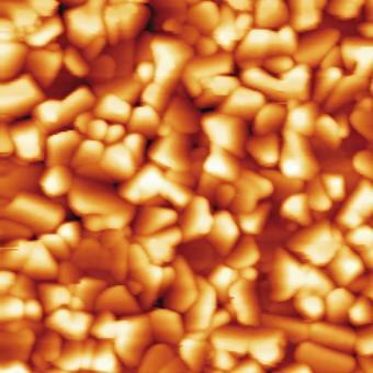
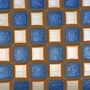
2 PZT thin film (Sol-gel) PZT thin film(mocvd) Au nano-particles DNA with atomic step Multi-walled CNT on glass Single-walled CNT on glass Hard disk data bits EFM/domain reversal Calibration Standard Hard disk surface Raster lithography/force modulation Raster lithography/indentation


 - Maximum number of pixel: Mega pixels/image (can set any pixel size from 8x8 to 9x9) -")


3 The n-tracer is complete SPM system designed for industrial users or researchers with optimal throughput and various application mode. Major application areas are high density data storage material science, life science, nanoscale device inspection. System Control Software Image Processing Software Standard Application Modes Software Highlight - Supports full SPM application modes in a single program - Supports image processing and analysis (D, flattening, surface/line analysis, etc. ) - Maximum number of pixel: Mega pixels/image (can set any pixel size from 8x8 to 9x9) - Real-time monitoring profile and FFT spectrum trace - Real-time color management - Quick zoom-in and penning of the scan area - Fully automated tuning of the DFM setup - Serial imaging mode / Bach spectroscopy mode - Adapted scanning technique - Real-time image remapping for high speed scanning - Advanced nanolithography with convenient pattern editor - Contact Mode/Dynamic Force Microscopy - Lateral Force Microscopy - Magnetic Force Microscopy - Phase Contrast/Force Modulation Microscopy - Current Imaging Microscopy - XY Scope, I-V, D-E Hysteresis, Force Spectroscopy Tool Advanced Application Modes - High speed imaging with self-actuating probe - Nanolithography with vector and raster scan tool - Electrostatic Force Microscopy - Scanning Tunneling Microscopy - Dynamic Q-controlled DFM mode


 Height = nm -")
![Z[nm] Z[nm] Z[nm] - -.](/docs-images/78/77161244/images/4-5.jpg "- - - 8-9 8 9 8 9 X[um] X[um]")
![X[um].](/docs-images/78/77161244/images/4-6.jpg "k k k High Speed and High Pixel")
 Frequency")

![um.um [Hz, rescan with X Points].](/docs-images/78/77161244/images/4-9.jpg "um.um Voltage (V) Plots show a")


4 High Speed Imaging Hz, x Points High Speed Probe Hz, x Points Hz, x Points Z Hz, x Points Z PZT actuator Hz, x Points Hz, x Points point, Hz Hz, x Points point, Hz 8Hz, x Points Si tip point, 8Hz Piezoresitive sensor Amplitude ( ) Height = nm - Z[nm] Z[nm] Z[nm] X[um] X[um] X[um]. k k k High Speed and High Pixel Imaging st Zoom-in Software Zoom in Displacement( ) Frequency (Hz) upward sweep downward sweep.um.um rd Zoom-in.um nd Zoom-in.um.um [Hz, rescan with X Points].um.um Voltage (V) Plots show a mechanical resonance and DC actuation characteristics of a micro actuator. The mechanical resonance frequency is about khz, and it can be actuated up to um to um with a small driving voltage.


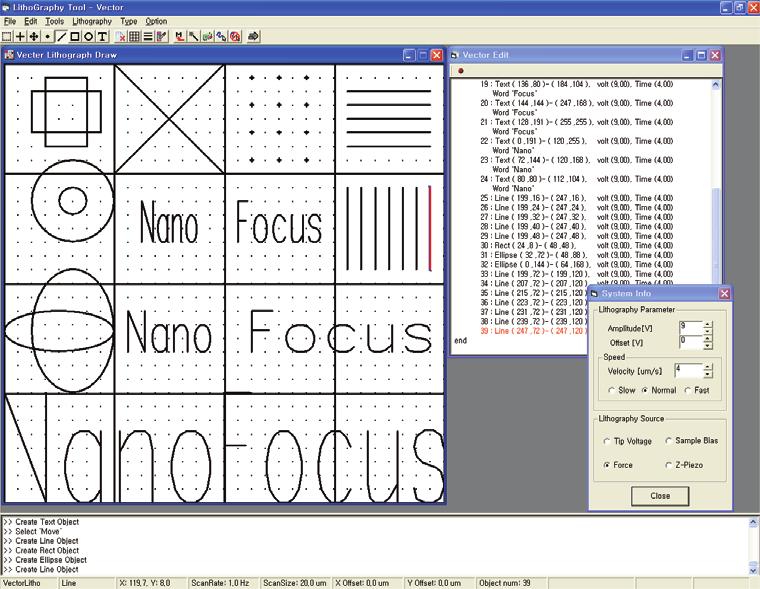
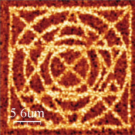
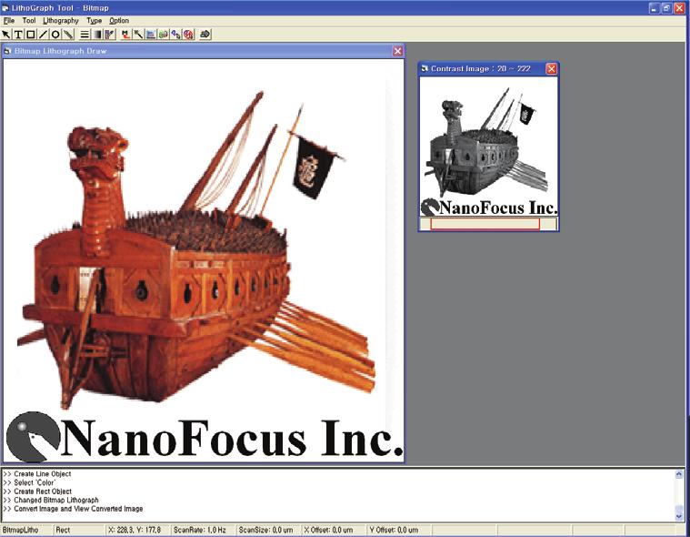
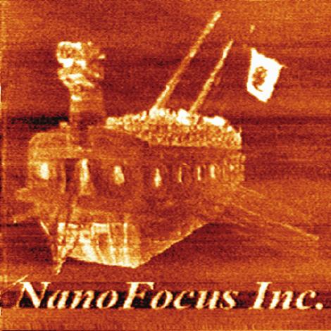
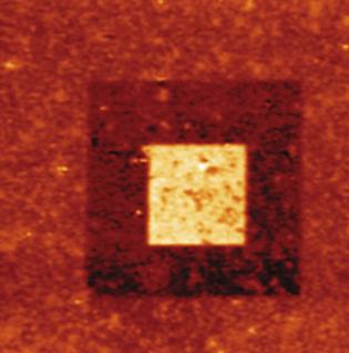
5 Dependence of Indentation Amplitude(Z-Piezo).um Indentation and scratching method/vector scan Vector/Raster Lithography Software.um Polarization reversal on ferroelectric thin film Oxidation on Ti thin film Indentation method/raster scan Mode.8um.um.um


6 Carbon nanotube (CNT) probe ¾ Strong and wear-resistant ¾ Sharp end and high-aspect ratio ¾ Shows gentle probe-sample interaction for imaging biological sample ¾ Increasing resolution and reliability ¾ Shows a good stability and performance while the SPM is operated. Specifications ¾ Length :, nm ¾ Diameter : ~ nm ¾ Angle deviation : (Cohesion aspect) (Side aspect)
NanoFocus Inc. Next Generation Scanning Probe Technology. Tel : Fax:
 NanoFocus Inc. Next Generation Scanning Probe Technology www.nanofocus.kr Tel : 82-2-864-3955 Fax: 82-2-864-3956 Albatross SPM is Multi functional research grade system Flexure scanner and closed-loop
Cutting-edge Atomic Force Microscopy techniques for large and multiple samples
 Cutting-edge Atomic Force Microscopy techniques for large and multiple samples Study of up to 200 mm samples using the widest set of AFM modes Industrial standards of automation A unique combination of
Measurement of Microscopic Three-dimensional Profiles with High Accuracy and Simple Operation
 238 Hitachi Review Vol. 65 (2016), No. 7 Featured Articles Measurement of Microscopic Three-dimensional Profiles with High Accuracy and Simple Operation AFM5500M Scanning Probe Microscope Satoshi Hasumura
Advanced Nanoscale Metrology with AFM
 Advanced Nanoscale Metrology with AFM Sang-il Park Corp. SPM: the Key to the Nano World Initiated by the invention of STM in 1982. By G. Binnig, H. Rohrer, Ch. Gerber at IBM Zürich. Expanded by the invention
Investigate in magnetic micro and nano structures by Magnetic Force Microscopy (MFM)
") Investigate in magnetic micro and nano 5.3.85- Related Topics Magnetic Forces, Magnetic Force Microscopy (MFM), phase contrast imaging, vibration amplitude, resonance shift, force Principle Caution! -
Investigate in magnetic micro and nano 5.3.85- Related Topics Magnetic Forces, Magnetic Force Microscopy (MFM), phase contrast imaging, vibration amplitude, resonance shift, force Principle Caution! -
- Near Field Scanning Optical Microscopy - Electrostatic Force Microscopy - Magnetic Force Microscopy
 - Near Field Scanning Optical Microscopy - Electrostatic Force Microscopy - Magnetic Force Microscopy Yongho Seo Near-field Photonics Group Leader Wonho Jhe Director School of Physics and Center for Near-field
Atomic Force Microscopy (Bruker MultiMode Nanoscope IIIA)
") Atomic Force Microscopy (Bruker MultiMode Nanoscope IIIA) This operating procedure intends to provide guidance for general measurements with the AFM. For more advanced measurements or measurements with
Atomic Force Microscopy (Bruker MultiMode Nanoscope IIIA) This operating procedure intends to provide guidance for general measurements with the AFM. For more advanced measurements or measurements with
INDIAN INSTITUTE OF TECHNOLOGY BOMBAY
 IIT Bombay requests quotations for a high frequency conducting-atomic Force Microscope (c-afm) instrument to be set up as a Central Facility for a wide range of experimental requirements. The instrument
Outline: Introduction: What is SPM, history STM AFM Image treatment Advanced SPM techniques Applications in semiconductor research and industry
 1 Outline: Introduction: What is SPM, history STM AFM Image treatment Advanced SPM techniques Applications in semiconductor research and industry 2 Back to our solutions: The main problem: How to get nm
SUPRA Optix 3D Optical Profiler
 SUPRA Optix 3D Optical Profiler Scanning White-light Interferometric Microscope SWIM Series Applications The SUPRA Optix is the latest development in the field of Scanning White-light Interferometry. With
Nanosurf Nanite. Automated AFM for Industry & Research.
 Nanosurf Nanite Automated AFM for Industry & Research www.nanosurf.com Multiple Measurements Automated Got work? Nanosurf has the solution! The Swiss-based innovator and manufacturer of the most compact
Basic methods in imaging of micro and nano structures with atomic force microscopy (AFM)
") Basic methods in imaging of micro and nano P2538000 AFM Theory The basic principle of AFM is very simple. The AFM detects the force interaction between a sample and a very tiny tip (
Basic methods in imaging of micro and nano P2538000 AFM Theory The basic principle of AFM is very simple. The AFM detects the force interaction between a sample and a very tiny tip (
Nanosurf easyscan 2 FlexAFM
 Nanosurf easyscan 2 FlexAFM Your Versatile AFM System for Materials and Life Science www.nanosurf.com The new Nanosurf easyscan 2 FlexAFM scan head makes measurements in liquid as simple as measuring in
Lecture 20: Optical Tools for MEMS Imaging
 MECH 466 Microelectromechanical Systems University of Victoria Dept. of Mechanical Engineering Lecture 20: Optical Tools for MEMS Imaging 1 Overview Optical Microscopes Video Microscopes Scanning Electron
Indian Institute of Technology Bombay
 Specifications for High Resolution Scanning Probe Microscope Item Essential measuring modes with complete hardware and software. All the modes should be demonstrated during installation & training Scanners
nanovea.com PROFILOMETERS 3D Non Contact Metrology
 PROFILOMETERS 3D Non Contact Metrology nanovea.com PROFILOMETER INTRO Nanovea 3D Non-Contact Profilometers are designed with leading edge optical pens using superior white light axial chromatism. Nano
Imaging Carbon Nanotubes Magdalena Preciado López, David Zahora, Monica Plisch
 Imaging Carbon Nanotubes Magdalena Preciado López, David Zahora, Monica Plisch I. Introduction In this lab you will image your carbon nanotube sample from last week with an atomic force microscope. You
Park NX-Hivac The world s most accurate and easy to use high vacuum AFM for failure analysis.
 Park NX-Hivac The world s most accurate and easy to use high vacuum AFM for failure analysis www.parkafm.com Park NX-Hivac High vacuum scanning for failure analysis applications 4 x 07 / Cm3 Current (µa)
UNIVERSITY OF WATERLOO Physics 360/460 Experiment #2 ATOMIC FORCE MICROSCOPY
 UNIVERSITY OF WATERLOO Physics 360/460 Experiment #2 ATOMIC FORCE MICROSCOPY References: http://virlab.virginia.edu/vl/home.htm (University of Virginia virtual lab. Click on the AFM link) An atomic force
Nanonics Systems are the Only SPMs that Allow for On-line Integration with Standard MicroRaman Geometries
 Nanonics Systems are the Only SPMs that Allow for On-line Integration with Standard MicroRaman Geometries 2002 Photonics Circle of Excellence Award PLC Ltd, England, a premier provider of Raman microspectral
Park NX20 The leading nano metrology tool for failure analysis and large sample research.
 The Most Accurate Atomic Force Microscope Park NX20 The leading nano metrology tool for failure analysis and large sample research www.parkafm.com The Most Accurate Atomic Force Microscope Park NX20 The
Standard Operating Procedure of Atomic Force Microscope (Anasys afm+)
") Standard Operating Procedure of Atomic Force Microscope (Anasys afm+) The Anasys Instruments afm+ system incorporates an Atomic Force Microscope which can scan the sample in the contact mode and generate
Standard Operating Procedure of Atomic Force Microscope (Anasys afm+) The Anasys Instruments afm+ system incorporates an Atomic Force Microscope which can scan the sample in the contact mode and generate
SPM The Industry s Performance Leader High Resolution Closed-loop System Fast, Easy Tip & Sample Exchange Versatility and Value Powerful Research
 SPM The Industry s Performance Leader High Resolution Closed-loop System Fast, Easy Tip & Sample Exchange Versatility and Value Powerful Research Flexibility Atomic resolution STM image of highly-oriented
Manufacturing Metrology Team
 The Team has a range of state-of-the-art equipment for the measurement of surface texture and form. We are happy to discuss potential measurement issues and collaborative research Manufacturing Metrology
AVI family The modular concept
 AVI350/LP AVI350LT/LP AVI400/LP AVI400LT/LP AVI600/LP AVI600LT/LP AVI350/LP AVI400/LP AVI600/LP Load (per unit) 0-200 kg 0-400 kg 0-600 kg Load (2 units) 0-400 kg 0-800 kg 0-1200 kg Static compliance vertically
Akiyama-Probe (A-Probe) guide
 guide") Akiyama-Probe (A-Probe) guide This guide presents: what is Akiyama-Probe, how it works, and what you can do Dynamic mode AFM Version: 2.0 Introduction NANOSENSORS Akiyama-Probe (A-Probe) is a self-sensing
Akiyama-Probe (A-Probe) guide This guide presents: what is Akiyama-Probe, how it works, and what you can do Dynamic mode AFM Version: 2.0 Introduction NANOSENSORS Akiyama-Probe (A-Probe) is a self-sensing
Nanotechnology Solutions Partner
 Nanotechnology Solutions Partner Park Systems Corp. KANC 4F, Iui-Dong 6-10, Suwon, Korea 443-270 Tel. +82-31-546-6800 Fax. +82-31-546-6805 www.parkafm.co.kr Park Systems Inc. 3040 Olcott St. Santa Clara,
Nanotechnology, the infrastructure, and IBM s research projects
 Nanotechnology, the infrastructure, and IBM s research projects Dr. Paul Seidler Coordinator Nanotechnology Center, IBM Research - Zurich Nanotechnology is the understanding and control of matter at dimensions
MEMS for RF, Micro Optics and Scanning Probe Nanotechnology Applications
 MEMS for RF, Micro Optics and Scanning Probe Nanotechnology Applications Part I: RF Applications Introductions and Motivations What are RF MEMS? Example Devices RFIC RFIC consists of Active components
LOW TEMPERATURE STM/AFM
 * CreaTec STM of Au(111) using a CO-terminated tip, 20mV bias, 0.6nA* LOW TEMPERATURE STM/AFM High end atomic imaging, spectroscopy and manipulation Designed and manufactured in Germany by CreaTec Fischer
Nanovie. Scanning Tunnelling Microscope
 Nanovie Scanning Tunnelling Microscope Nanovie STM Always at Hand Nanovie STM Lepto for Research Nanovie STM Educa for Education Nanovie Auto Tip Maker Nanovie STM Lepto Portable 3D nanoscale microscope
Akiyama-Probe (A-Probe) guide
 guide") Akiyama-Probe (A-Probe) guide This guide presents: what is Akiyama-Probe, how it works, and its performance. Akiyama-Probe is a patented technology. Version: 2009-03-23 Introduction NANOSENSORS Akiyama-Probe
Akiyama-Probe (A-Probe) guide This guide presents: what is Akiyama-Probe, how it works, and its performance. Akiyama-Probe is a patented technology. Version: 2009-03-23 Introduction NANOSENSORS Akiyama-Probe
The Most Accurate Atomic Force Microscope. Park NX20 The leading nano metrology tool for failure analysis and large sample research.
 The Most Accurate Atomic Force Microscope Park NX20 The leading nano metrology tool for failure analysis and large sample research www.parkafm.com Park Systems The Most Accurate Atomic Force Microscope
Indentation Cantilevers
 curve is recorded utilizing the DC displacement of the cantilever versus the extension of the scanner. Many indentations may be made using various forces, rates, etc. Upon exiting indentation mode, TappingMode
Nanosurf easyscan 2 Your Modular Scanning Probe Microscopy System
 Nanosurf Your Modular Scanning Probe Microscopy System www.nanosurf.com Perfect Modularity Nanosurf s easyscan series has gained worldwide popularity through its affordability, portability, and ease of
ATOMIC FORCE MICROSCOPY
 B47 Physikalisches Praktikum für Fortgeschrittene Supervision: Prof. Dr. Sabine Maier sabine.maier@physik.uni-erlangen.de ATOMIC FORCE MICROSCOPY Version: E1.4 first edit: 15/09/2015 last edit: 05/10/2018
PicoMaster 100. Unprecedented finesse in creating 3D micro structures. UV direct laser writer for maskless lithography
 UV direct laser writer for maskless lithography Unprecedented finesse in creating 3D micro structures Highest resolution in the market utilizing a 405 nm diode laser Structures as small as 300 nm 375 nm
AFM of High-Profile Surfaces
 AFM of High-Profile Surfaces Fig. 1. AFM topograpgy image of black Si made using SCD probe tip. Scan size 4. Profile height is more than 8. See details and other application examples below. High Aspect
Unit-25 Scanning Tunneling Microscope (STM)
") Unit-5 Scanning Tunneling Microscope (STM) Objective: Imaging formation of scanning tunneling microscope (STM) is due to tunneling effect of quantum physics, which is in nano scale. This experiment shows
Unit-5 Scanning Tunneling Microscope (STM) Objective: Imaging formation of scanning tunneling microscope (STM) is due to tunneling effect of quantum physics, which is in nano scale. This experiment shows
Prepare Sample 3.1. Place Sample in Stage. Replace Probe (optional) Align Laser 3.2. Probe Approach 3.3. Optimize Feedback 3.4. Scan Sample 3.
 Align Laser 3.2. Probe Approach 3.3. Optimize Feedback 3.4. Scan Sample 3.") CHAPTER 3 Measuring AFM Images Learning to operate an AFM well enough to get an image usually takes a few hours of instruction and practice. It takes 5 to 10 minutes to measure an image if the sample is
CHAPTER 3 Measuring AFM Images Learning to operate an AFM well enough to get an image usually takes a few hours of instruction and practice. It takes 5 to 10 minutes to measure an image if the sample is
Nanoscale Material Characterization with Differential Interferometric Atomic Force Microscopy
 Nanoscale Material Characterization with Differential Interferometric Atomic Force Microscopy F. Sarioglu, M. Liu, K. Vijayraghavan, A. Gellineau, O. Solgaard E. L. Ginzton Laboratory University Tip-sample
Figure for the aim4np Report
 Figure for the aim4np Report This file contains the figures to which reference is made in the text submitted to SESAM. There is one page per figure. At the beginning of the document, there is the front-page
Park XE7 The most affordable research grade AFM with flexible sample handling.
 Park XE7 The most affordable research grade AFM with flexible sample handling www.parkafm.com Park Systems The Most Accurate Atomic Force Microscope Park XE7 The economical choice for innovative research
The Most Accurate Atomic Force Microscope. Park XE15 Power and versatility, brilliantly combined.
 The Most Accurate Atomic Force Microscope Park XE15 Power and versatility, brilliantly combined. www.parkafm.com Park XE15 Increase your productivity with our powerfully versatile atomic force microscope
Microscopic Structures
 Microscopic Structures Image Analysis Metal, 3D Image (Red-Green) The microscopic methods range from dark field / bright field microscopy through polarisation- and inverse microscopy to techniques like
Nikon COOLSCAN V ED Major Features
 Nikon COOLSCAN V ED Major Features 4,000-dpi true optical-resolution scanning, 14-bit A/D converter featuring 16-/8-bit output for clear, colorful images Exclusive Scanner Nikkor ED high-performance lens
Introduction of New Products
 Field Emission Electron Microscope JEM-3100F For evaluation of materials in the fields of nanoscience and nanomaterials science, TEM is required to provide resolution and analytical capabilities that can
High Precision Positioning Mechanisms for a Hard X-ray Nanoprobe Instrument. Abstract
 High Precision Positioning Mechanisms for a Hard X-ray Nanoprobe Instrument D. Shu, J. Maser,, B. Lai, S. Vogt, M. Holt, C. Preissner, A. Smolyanitskiy,4, R. Winarski, and G. B. Stephenson,3 Center for
Surface Finish Measurement Methods and Instrumentation
 125 years of innovation Surface Finish Measurement Methods and Instrumentation Contents Visual Inspection Surface Finish Comparison Plates Contact Gauges Inductive / Variable Reluctance (INTRA) Piezo Electric
University of Nevada, Reno
 University of Nevada, Reno Design and Characterization of Scanning Probe Microscopy Platform with Active Electro-Thermal Microcantilever for Multifunctional Applications A thesis submitted in partial fulfillment
First Time User Manual
 Fiber Fabry-Perot Tunable Filter FFP-TF2 First Time User Manual Micron Optics Inc. 1852 Century Place NE Atlanta, GA 30345 USA phone 404 325 0005 fax 404 325 4082 www.micronoptics.com Copyright 2009 Micron
M-041 M-044 Tip/Tilt Stage
 M-041 M-044 Tip/Tilt Stage Piezo Drive Option for Nanometer Precision Ordering Information Linear Actuators & Motors M-041.00 Small Tilt Stage, Manual Micrometer Drive M-041.D01 Small Tilt Stage, DC-Motor
3D Optical Motion Analysis of Micro Systems. Heinrich Steger, Polytec GmbH, Waldbronn
 3D Optical Motion Analysis of Micro Systems Heinrich Steger, Polytec GmbH, Waldbronn SEMICON Europe 2012 Outline Needs and Challenges of measuring Micro Structure and MEMS Tools and Applications for optical
Microscopic Laser Doppler Vibrometer
 Microscopic Laser Doppler Vibrometer System Configuration - 1 PC Controller (APU-Analog processing unit, DPU-Digital processing unit) Optic Head (MEMS Type, XS Type) Function Generator Power Supply Testing
Scanning Tunneling Microscopy
 Scanning Tunneling Microscopy The wavelike properties of electrons allows them to tunnel beyond the regions of a solid into a region of space forbidden for them to exist in. In this region they can be
Nanodrawing of Aligned Single Carbon. Nanotubes with a Nanopen
 Supporting Information Nanodrawing of Aligned Single Carbon Nanotubes with a Nanopen Talia Yeshua, 1,2 Christian Lehmann, 3 Uwe Hübner, 4 Suzanna Azoubel, 2,5 Shlomo Magdassi, 2,5 Eleanor E. B. Campbell,
Scanning Microwave. Expanding Impedance Measurements to the Nanoscale: Coupling the Power of Scanning Probe Microscopy with the PNA
 Agilent Technologies Scanning Microwave Microscopy (SMM) Expanding Impedance Measurements to the Nanoscale: Coupling the Power of Scanning Probe Microscopy with the PNA Presented by: Craig Wall PhD Product
Electric polarization properties of single bacteria measured with electrostatic force microscopy
 Electric polarization properties of single bacteria measured with electrostatic force microscopy Theoretical and practical studies of Dielectric constant of single bacteria and smaller elements Daniel
Nikon SUPER COOLSCAN 5000 ED Major Features
 Nikon SUPER COOLSCAN 5000 ED Major Features 4,000-dpi true optical-resolution scanning, 16-bit A/D converter featuring 16-/8-bit output for crisp, color-true images Exclusive Scanner Nikkor ED high-performance
attosnom I: Topography and Force Images NANOSCOPY APPLICATION NOTE M06 RELATED PRODUCTS G
 APPLICATION NOTE M06 attosnom I: Topography and Force Images Scanning near-field optical microscopy is the outstanding technique to simultaneously measure the topography and the optical contrast of a sample.
Zeta-300 3D OPTICAL PROFILER
 Zeta-300 3D OPTICAL PROFILER Technology Toolkit Developed in 2007, the revolutionary Confocal Grid Structured Illumination (CGSI) is the powerful technology in all Zeta Optical Profilers but in a Zeta,
EMC-scanner. HRE-series. See it before you CE it!
 EMC-scanner HRE-series See it before you CE it! Print Screen image of a scan measurement. Seeing high frequencies! Now you can SEE high frequency electro magnetic fields. The background There are high
LaserBeam ProfilingSolutions. IRLaserBeam Profiler
 LaserBeam ProfilingSolutions IRLaserBeam Profiler TABLE OF CONTENTS PRODUCT DESCRIPTION LASERDEC CL200 TECHNICAL DATA DIMENSIONS LASERDEC CL500 TECHNICAL DATA DIMENSIONS LASERDEC CR200 TECHNICAL DATA DIMENSIONS
Keysight Technologies Scanning Microwave Microscope Mode. Application Note
 Keysight Technologies Scanning Microwave Microscope Mode Application Note Introduction Measuring electromagnetic properties of materials can provide insight into applications in many areas of science and
Controller Design for Z Axis Movement of STM Using SPM Control Software
 Controller Design for Z Axis Movement of STM Using SPM Control Software Neena Tom, Rini Jones S. B Abstract Scanning probe microscopy is a branch of microscopy that forms images of surfaces using a physical
TF TF Analyzer 2000 Measurement System
 TF Analyzer 2000 Measurement System The TF Analyzer 2000 is the most sophisticated analyzer of electroceramic material and devices. The test equipment is based on a modular idea, where four different probe
Systematic Workflow via Intuitive GUI. Easy operation accomplishes your goals faster than ever.
 Systematic Workflow via Intuitive GUI Easy operation accomplishes your goals faster than ever. 16 With the LEXT OLS4100, observation or measurement begins immediately once the sample is placed on the stage.
Coherent Laser Measurement and Control Beam Diagnostics
 Coherent Laser Measurement and Control M 2 Propagation Analyzer Measurement and display of CW laser divergence, M 2 (or k) and astigmatism sizes 0.2 mm to 25 mm Wavelengths from 220 nm to 15 µm Determination
SENSOR+TEST Conference SENSOR 2009 Proceedings II
 B8.4 Optical 3D Measurement of Micro Structures Ettemeyer, Andreas; Marxer, Michael; Keferstein, Claus NTB Interstaatliche Hochschule für Technik Buchs Werdenbergstr. 4, 8471 Buchs, Switzerland Introduction
Development of innovative fringe locking strategies for vibration-resistant white light vertical scanning interferometry (VSI)
") Development of innovative fringe locking strategies for vibration-resistant white light vertical scanning interferometry (VSI) Liang-Chia Chen 1), Abraham Mario Tapilouw 1), Sheng-Lih Yeh 2), Shih-Tsong
Development of innovative fringe locking strategies for vibration-resistant white light vertical scanning interferometry (VSI) Liang-Chia Chen 1), Abraham Mario Tapilouw 1), Sheng-Lih Yeh 2), Shih-Tsong
Profile Measurement of Resist Surface Using Multi-Array-Probe System
 Sensors & Transducers 2014 by IFSA Publishing, S. L. http://www.sensorsportal.com Profile Measurement of Resist Surface Using Multi-Array-Probe System Shujie LIU, Yuanliang ZHANG and Zuolan YUAN School
The old adage seeing is believing is appropriate when
 26 Quality Digest/October 2001 The old adage seeing is believing is appropriate when referring to optical comparators. Because these measurement tools display a magnified image of a part, a tremendous
Difrotec Product & Services. Ultra high accuracy interferometry & custom optical solutions
 Difrotec Product & Services Ultra high accuracy interferometry & custom optical solutions Content 1. Overview 2. Interferometer D7 3. Benefits 4. Measurements 5. Specifications 6. Applications 7. Cases
Department of Physics
 UNIVERSITY OF CALICUT Calicut University PO Thenjipalam, Malappuram Dist Kerala 673 635, India Department of Physics No. DP/46/FIST-II/2011 05/11/2011 TENDER NOTICE Sealed competitive tenders are invited
Large Signal Displacement Measurement with an Asylum SA Atomic Force Microscope Rev B
 Radiant Technologies, Inc. 2835D Pan American Freeway NE Albuquerque, NM 87107 Tel: 505-842-8007 Fax: 505-842-0366 e-mail: radiant@ferrodevices.com www.ferrodevices.com Large Signal Displacement Measurement
Zeta-20. Zeta3D OPTICAL PROFILER IMAGING THE IMPOSSIBLE
 Zeta3D OPTICAL PROFILER Zeta-20 IMAGING THE IMPOSSIBLE TRUE COLOR 3D DIC BRIGHT FIELD DARK FIELD POLARIZED LIGHT IMAGE THROUGH TRANSMISSIVE IMAGE WHITE OR BLUE LED LIGHT SOURCE THIN FILM THICKNESS DIAMOND
Standard Operating Procedure
 Standard Operating Procedure Nanosurf Atomic Force Microscopy Operation Facility NCCRD Nanotechnology Center for Collaborative Research and Development Department of Chemistry and Engineering Physics The
V2018 SPINSTAND AND NEW SERVO-8 SYSTEM
 34 http://www.guzik.com/products/head-and-media-disk-drive-test/spinstands/ V2018 SPINSTAND AND NEW SERVO-8 SYSTEM Designed for Automated High-TPI HGA Volume Testing Up to 1300 ktpi Estimated Capability
SUPPLEMENTARY INFORMATION
 Figure S. Experimental set-up www.nature.com/nature Figure S2. Dependence of ESR frequencies (GHz) on a magnetic field (G) applied in different directions with respect to NV axis ( θ 2π). The angle with
Near-field Optical Microscopy
 Near-field Optical Microscopy R. Fernandez, X. Wang, N. Li, K. Parker, and A. La Rosa Physics Department Portland State University Portland, Oregon Near-Field SPIE Optics Microscopy East 2005 Group PSU
Park NX10. The most accurate and easiest to use Atomic Force Microscope.
 The most accurate and easiest to use Atomic Force Microscope www.parkafm.com Park Systems Enabling Nanoscale Advances The premiere choice for nanotechnology research Better data Park NX10 produces data
Ionscope SICM. About Ionscope. Scanning Ion Conductance Microscopy. Ionscope A brand of Openiolabs Limited
 SICM About is a brand of openiolabs Ltd, headquartered in Cambridge UK, is the world-leader in (SICM), a rapidly emerging Scanning Probe Microscopy (SPM) technique which allows nanoscale topographical
Measurement of Surface Profile and Layer Cross-section with Wide Field of View and High Precision
 Hitachi Review Vol. 65 (2016), No. 7 243 Featured Articles Measurement of Surface Profile and Layer Cross-section with Wide Field of View and High Precision VS1000 Series Coherence Scanning Interferometer
Large Signal Displacement Measurement with an MTI Photonic Sensor Rev B
 Radiant Technologies, Inc. 2835D Pan American Freeway NE Albuquerque, NM 8717 Tel: 55-842-87 Fax: 55-842-366 e-mail: radiant@ferrodevices.com www.ferrodevices.com Large Signal Displacement Measurement
MAR2100 MARADIN MEMS DRIVE AND CONTROL
 MAR2100 MARADIN MEMS DRIVE AND CONTROL The MAR2100 is a Drive and control IC for Maradin's MAR1100 dual-axis MEMS based scanning mirror. MAR2100 is targeted for miniature laser projectors and laser steering
University of MN, Minnesota Nano Center Standard Operating Procedure
 Equipment Name: Atomic Force Microscope Badger name: afm DI5000 PAN Revisionist Paul Kimani Model: Dimension 5000 Date: October 6, 2017 Location: Bay 1 PAN Revision: 1 A. Description i. Enhanced Motorized
Laser Speckle Reducer LSR-3000 Series
 Datasheet: LSR-3000 Series Update: 06.08.2012 Copyright 2012 Optotune Laser Speckle Reducer LSR-3000 Series Speckle noise from a laser-based system is reduced by dynamically diffusing the laser beam. A
Innovative Technology for Innovative Science Hands-on in a Nanoscience Classroom
 Innovative Technology for Innovative Science Hands-on in a Nanoscience Classroom Presented by Jennifer F. Wall, Ph.D. Imaging Possibilities Optical 2 mm Electron 500 microns Atomic Force 10 microns Scanning
; A=4π(2m) 1/2 /h. exp (Fowler Nordheim Eq.) 2 const
 1/2 /h. exp (Fowler Nordheim Eq.) 2 const") Scanning Tunneling Microscopy (STM) Brief background: In 1981, G. Binnig, H. Rohrer, Ch. Gerber and J. Weibel observed vacuum tunneling of electrons between a sharp tip and a platinum surface. The tunnel
Scanning Tunneling Microscopy (STM) Brief background: In 1981, G. Binnig, H. Rohrer, Ch. Gerber and J. Weibel observed vacuum tunneling of electrons between a sharp tip and a platinum surface. The tunnel
Definitions. Spectrum Analyzer
 SIGNAL ANALYZERS Spectrum Analyzer Definitions A spectrum analyzer measures the magnitude of an input signal versus frequency within the full frequency range of the instrument. The primary use is to measure
Nano Beam Position Monitor
 Introduction Transparent X-ray beam monitoring and imaging is a new enabling technology that will become the gold standard tool for beam characterisation at synchrotron radiation facilities. It allows
Park NX-Hivac: Phase-lock Loop for Frequency Modulation Non-Contact AFM
 Park Atomic Force Microscopy Application note #21 www.parkafm.com Hosung Seo, Dan Goo and Gordon Jung, Park Systems Corporation Romain Stomp and James Wei Zurich Instruments Park NX-Hivac: Phase-lock Loop
Study of shear force as a distance regulation mechanism for scanning near-field optical microscopy
 Study of shear force as a distance regulation mechanism for scanning near-field optical microscopy C. Durkan a) and I. V. Shvets Department of Physics, Trinity College Dublin, Ireland Received 31 May 1995;
Bruker Dimension Icon AFM Quick User s Guide
 Bruker Dimension Icon AFM Quick User s Guide March 3, 2015 GLA Contacts Jingjing Jiang (jjiang2@caltech.edu 626-616-6357) Xinghao Zhou (xzzhou@caltech.edu 626-375-0855) Bruker Tech Support (AFMSupport@bruker-nano.com
EM-ISight Electromagnetic Scanning System. Since Page 1 of 6 Phone (613) Fax (613)
 Fax (613)") Since 1981 EM-ISight Electromagnetic Scanning System Page 1 of 6 EM-ISight ALSAS EM7 APREL Laboratories is a pioneer in the area of automated system solutions and is pleased to introduce EM-ISight which,
Since 1981 EM-ISight Electromagnetic Scanning System Page 1 of 6 EM-ISight ALSAS EM7 APREL Laboratories is a pioneer in the area of automated system solutions and is pleased to introduce EM-ISight which,
By: Louise Brown, PhD, Advanced Engineered Materials Group, National Physical Laboratory.
 NPL The Olympus LEXT - A highly flexible tool Confocal Metrology at the NPL By: Louise Brown, PhD, Advanced Engineered Materials Group, National Physical Laboratory. www.npl.co.uk louise.brown@npl.co.uk
Panasonic, 2 Channel FFT Analyzer VS-3321A. DC to 200kHz,512K word memory,and 2sets of FDD
 Panasonic, 2 Channel FFT Analyzer VS-3321A DC to 200kHz,512K word memory,and 2sets of FDD New generation 2CH FFT Anal General The FFT analyzer is a realtime signal analyzer using the Fast Fourier Transform
Micro-manipulated Cryogenic & Vacuum Probe Systems
 Janis micro-manipulated probe stations are designed for non-destructive electrical testing using DC, RF, and fiber-optic probes. They are useful in a variety of fields including semiconductors, MEMS, superconductivity,
THE ULTIMATE DOCUMENT EXAMINATION SYSTEM STATE-OF-THE-ART SPECTRAL ANALYSIS FORENSIC LABS SECURITY PRINTERS IMMIGRATION AUTHORITIES
 THE ULTIMATE DOCUMENT EXAMINATION SYSTEM STATE-OF-THE-ART SPECTRAL ANALYSIS FORENSIC LABS SECURITY PRINTERS IMMIGRATION AUTHORITIES WHEN DETAILS MATTER PROJECTINA SPECTRA PRO The Ultimate Document Examination
ezafm OPERATING MANUAL
 ezafm OPERATING MANUAL 2013rev 2.0 1 Table of Contents CHAPTER 1:ezAFM... 4 1.1. Introduction... 5 1.2. System Components... 5 1.3. Unpacking and Packing the Instrument... 6 1.3.1. Before Installation...