Nanoscale Material Characterization with Differential Interferometric Atomic Force Microscopy
|
|
|
- Todd Grant
- 5 years ago
- Views:
Transcription


1 Nanoscale Material Characterization with Differential Interferometric Atomic Force Microscopy F. Sarioglu, M. Liu, K. Vijayraghavan, A. Gellineau, O. Solgaard E. L. Ginzton Laboratory University Tip-sample Interaction in TM-AFM Repulsive Regime Force 0 Attractive Regime Tip-sample distance Dynamic tip-sample interaction Attractive Regime van der Waals Forces, Magnetic Forces, Electrical Forces Repulsive Regime Elasticity 1
 Use of torsional mode to increase the bandwidth Can capture a set of interaction force harmonics with improved SNR HarmoniX Nanoscale Material Property Mapping Full-spectrum harmonic image")
2 High-bandwidth Force Probes Coupled Torsional Cantilevers (Sahin et. al 2007) Use of torsional mode to increase the bandwidth Can capture a set of interaction force harmonics with improved SNR HarmoniX Nanoscale Material Property Mapping Full-spectrum harmonic image processing. High Resolution, Realtime Quanitative results Increased bandwidth require better signal to avoid lowering the SNR High-Frequency Force-Sensing AFM Probes An AFM probe that can measure tip-sample interaction forces during tapping-mode AFM (TM - AFM) imaging High-bandwidth force sensor provides increased temporal resolution Soft cantilever provides gentle resonant interaction with the surface 2

*λ/8 displacement (2n-1)*λ/4")
 0 0.4 0.45 0.5 0.55 0.6 Position (a.u.) 0 0.4 0.45 0.5 0.55 0.6 Position (a.u.) 3")
3 Displacement sensor Interferometric relative displacement sensor for tip motion Phase-sensitive diffraction grating λ/8 offset is required for maximum sensitivity and linearity 0 th order 1 st order z Displacement sensor Light intensity of even modes is maximized when the displacement is an even integer multiple of λ/4 Light intensity of odd modes are maximized when the displacement is an odd integer multiple of λ/4 n*λ/2 displacement (2n-1)*λ/8 displacement (2n-1)*λ/4 displacement Light intensity (a.u.) Light intensity (a.u.) Light intensity (a.u.) Position (a.u.) Position (a.u.) Position (a.u.) 3


4 Mechanical Bandwidth A conventional AFM cantilever can not fully capture the high frequency tip-sample interaction in tapping-mode AFM Cantilever Fundamental Resonance Cantilever Drive Frequency Sensor Fundamental Resonance Cantilever Drive Frequency Probe with an integrated sensor An integrated high bandwidth force sensor on the cantilever k cantilever Cantilever k tip Tip F tip-sample 4

 wafer")
5 Cantilever flexural resonances Mechanical design Sensor Reference Cantilever oscillations couple to the differential grating signal Coupling can be minimized by making the outer moving fingers shorter Sensor transfer function can be approximated as a simple harmonic oscillator Start with an SOI (silicon on insulator) wafer Fabrication 5
6 Fabrication Grow thermal oxide Deposit LPCVD silicon nitride Fabrication Pattern silicon nitride layer with plasma etch Grow thermal oxide 6


7 Fabrication Etch silicon nitride in H 3 PO 4 Etch oxide in HF Fabrication Bond an oxidized DSP (double-sidepolished) wafer on patterned SOI device layer Anneal at 1050C 7

8 Fabrication Etch SOI handle wafer using TMAH (tetra methyl ammonium hydroxide) Fabrication Deposit LPCVD silicon nitride Pattern silicon nitride layer using plasma etch Pattern oxide layer using HF 8
9 Form tip and support regions using isotropic dry etch Fabrication Remove oxide layer using HF Fabrication 9
10 Oxidize at 950C to sharpen the tip Fabrication Pattern oxide layer Etch device layer to form the cantilever outline Fabrication 10

11 Fabrication Deposit TEOS (tetraethyl orthosilicate) Deposit LPCVD silicon nitride Pattern backside silicon nitride layer Etch handle wafer using KOH Fabrication Etch silicon nitride in a plasma etch Etch oxide in HF to release the cantilever 11


12 Fabricated Cantilevers Height offset Set of cantilevers optimized for different materials Ratio of Sensor resonance to cantilever resonance varies from quadrant photodiode Probe Operation Lateral = relative tip displacement Vertical = cantilever oscillation Individual tapping events can be identified The ringing is due to the force sensor resonance The sensor is ~18x faster than the cantilever body 12

 TEOS Pt Topography image 10 th")

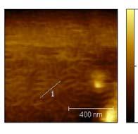
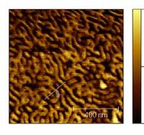
13 Imaging Setup Cantilever Drive Signal Phase Detector Phase Image Quad Cell Photodiode Cantilever Oscillation Feedback Control Electronics Topography Laser diode Piezo tube Force Signal Lock-in Amplifier Harmonic Image Computer f Material Mapping Ion beam assisted deposition Platinum, Tetraethyl orthosilicate (TEOS) TEOS Pt Topography image 10 th harmonic image SEM image Harmonic image reveals checkerboard pattern due to difference in the tip-sample interaction Increased spatial resolution for the samples with large topographical differences 13


 -20-30 -40-50 -60-70")
 Cantilever is")


14 Topography image C 18 SAM on Gold Phase Image 18 th harmonic image Vertical and horizontal states have different mechanical properties Tip-sample interaction measurements Oscilloscope trace 0-10 Frequency spectrum Signal Power (dbm) Frequency (MHz) Cantilever is driven on resonance The sensor is ~30x faster than the cantilever body Spectrum contains harmonics of the drive signal with high SNR Cantilever drive frequency 14


 Equipartition")
15 Measurement of ω s and Q Tip Displacement Cantilever Displacement By observing a single tip-sample rupture event, the resonance frequency and the quality factor of the force sensor are measured. Spring Constant Calibration Thermal spectrum is measured at the room temperature Cantilever fundamental resonance peak Displacement (m) Equipartition theorem mω 0 q = k T 2 2 B Frequency (Hz) 15
 Piezotube Input Time (s) Laser diode Piezotube Detector Output (V) 0 th")
 Time (s) Signal Processing k, ω s and Q Calibration")
 sin(2ω 0 t)")
16 Calibration Calibration is performed to convert photodetector output to force values Displacement (nm) Piezotube Input Time (s) Laser diode Piezotube Detector Output (V) 0 th mode Time (s) Dual cell photodiode Hard sample - + Detector Output (V) 1 st mode Time (s) 0 th mode 1 st mode Detector Output (V) Time (s) Signal Processing k, ω s and Q Calibration Parameters Inverse Filter Force signal Average FFT IFFT Peak Repulsive Force Peak Attractive Force Max Min + - Labview program Calculations are done in 2-4 ms sin(ω 0 t) sin(2ω 0 t) sin(nω 0 t) 16


 Peak repulsive force Peak")


17 Force Imaging Setup Quad Cell Photodiode Laser diode Cantilever Oscillation Feedback Control Electronics Computer Piezo tube Force Signal DAQ Card Force Image F repulsive F attractive Adhesive carbon tape 6 um Topography image Amplitude Phase image 13 th harmonic (amp) 13 th harmonic (phase) Peak repulsive force Peak adhesive force The adhesive force map identifies the particles that are responsible for adhesion and show a range of different adhesion forces 17
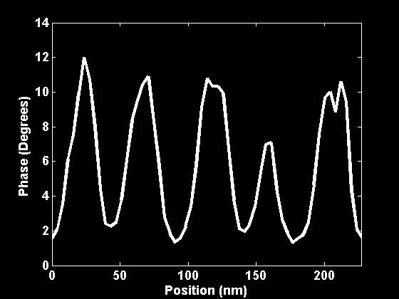
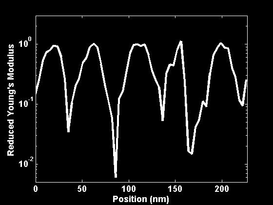
18 SBS triblock copolymer Polystyrene-polybutadiene-polystyrene - Periodicity ~ 40nm Bulk Young s Modulus (room temp): Polystyrene ~ 2-4 GPa, Polybutadiene ~ 1MPa Topography 8.1 nm Phase 17.1 o Reduced Young s Modulus 1.54 GPa -5 nm 0.6 o 0 Harmonic Imaging in Liquids Topography image Phase Image 10 th harmonic image In liquid, the effect of dissipative processes due to adhesion on the surface disappears The phase image can not differentiate between the two surfaces The elasticity difference between materials creates the contrast in the harmonic image 18
19 Summary Designed and fabricated cantilevers that can measure high-frequency tip-sample forces with high force sensitivity and high temporal resolution Demonstrated high contrast compositional mapping by utilizing harmonics of the tip displacement Imaging in air and in water Demonstrated quantitative nanoscale material characterization by measuring reduced Young s modulus of the tip-sample contact Acknowledgements: Dr. Sergei Magonov - SBS polymer sample Agilent Technologies Funding and Equipment support NSF, CPN, DARPA, Center for Integrated Systems 19
Outline: Introduction: What is SPM, history STM AFM Image treatment Advanced SPM techniques Applications in semiconductor research and industry
 1 Outline: Introduction: What is SPM, history STM AFM Image treatment Advanced SPM techniques Applications in semiconductor research and industry 2 Back to our solutions: The main problem: How to get nm
Atomic Force Microscopy (Bruker MultiMode Nanoscope IIIA)
") Atomic Force Microscopy (Bruker MultiMode Nanoscope IIIA) This operating procedure intends to provide guidance for general measurements with the AFM. For more advanced measurements or measurements with
Atomic Force Microscopy (Bruker MultiMode Nanoscope IIIA) This operating procedure intends to provide guidance for general measurements with the AFM. For more advanced measurements or measurements with
PROBLEM SET #7. EEC247B / ME C218 INTRODUCTION TO MEMS DESIGN SPRING 2015 C. Nguyen. Issued: Monday, April 27, 2015
 Issued: Monday, April 27, 2015 PROBLEM SET #7 Due (at 9 a.m.): Friday, May 8, 2015, in the EE C247B HW box near 125 Cory. Gyroscopes are inertial sensors that measure rotation rate, which is an extremely
Lateral Force: F L = k L * x
 Scanning Force Microscopy (SFM): Conventional SFM Application: Topography measurements Force: F N = k N * k N Ppring constant: Spring deflection: Pieo Scanner Interaction or force dampening field Contact
; A=4π(2m) 1/2 /h. exp (Fowler Nordheim Eq.) 2 const
 1/2 /h. exp (Fowler Nordheim Eq.) 2 const") Scanning Tunneling Microscopy (STM) Brief background: In 1981, G. Binnig, H. Rohrer, Ch. Gerber and J. Weibel observed vacuum tunneling of electrons between a sharp tip and a platinum surface. The tunnel
Scanning Tunneling Microscopy (STM) Brief background: In 1981, G. Binnig, H. Rohrer, Ch. Gerber and J. Weibel observed vacuum tunneling of electrons between a sharp tip and a platinum surface. The tunnel
Park NX-Hivac: Phase-lock Loop for Frequency Modulation Non-Contact AFM
 Park Atomic Force Microscopy Application note #21 www.parkafm.com Hosung Seo, Dan Goo and Gordon Jung, Park Systems Corporation Romain Stomp and James Wei Zurich Instruments Park NX-Hivac: Phase-lock Loop
- Near Field Scanning Optical Microscopy - Electrostatic Force Microscopy - Magnetic Force Microscopy
 - Near Field Scanning Optical Microscopy - Electrostatic Force Microscopy - Magnetic Force Microscopy Yongho Seo Near-field Photonics Group Leader Wonho Jhe Director School of Physics and Center for Near-field
Atomic Force Microscopy (I)
") Atomic Force Microscopy (I) - Optical Grating AFM and the thermal noise measurement 2.674 Lab 10 Spring 2016 Pappalardo II Micro/Nano Laboratories AFM Imaging (with home-made AFMs) I. Safety Notes This
Atomic Force Microscopy (I) - Optical Grating AFM and the thermal noise measurement 2.674 Lab 10 Spring 2016 Pappalardo II Micro/Nano Laboratories AFM Imaging (with home-made AFMs) I. Safety Notes This
Electronic Characterization of Materials Using Conductive AFM
 Electronic Characterization of Materials Using Conductive AFM Amir Moshar Electrical Measurements SKPM EFM CAFM PFM SCM Non-Contact Electrical Techniques Scanning Kelvin Probe Microscopy Electric Force
Basic methods in imaging of micro and nano structures with atomic force microscopy (AFM)
") Basic methods in imaging of micro and nano P2538000 AFM Theory The basic principle of AFM is very simple. The AFM detects the force interaction between a sample and a very tiny tip (
Basic methods in imaging of micro and nano P2538000 AFM Theory The basic principle of AFM is very simple. The AFM detects the force interaction between a sample and a very tiny tip (
Microscopic Structures
 Microscopic Structures Image Analysis Metal, 3D Image (Red-Green) The microscopic methods range from dark field / bright field microscopy through polarisation- and inverse microscopy to techniques like
Cutting-edge Atomic Force Microscopy techniques for large and multiple samples
 Cutting-edge Atomic Force Microscopy techniques for large and multiple samples Study of up to 200 mm samples using the widest set of AFM modes Industrial standards of automation A unique combination of
attosnom I: Topography and Force Images NANOSCOPY APPLICATION NOTE M06 RELATED PRODUCTS G
 APPLICATION NOTE M06 attosnom I: Topography and Force Images Scanning near-field optical microscopy is the outstanding technique to simultaneously measure the topography and the optical contrast of a sample.
Lecture 20: Optical Tools for MEMS Imaging
 MECH 466 Microelectromechanical Systems University of Victoria Dept. of Mechanical Engineering Lecture 20: Optical Tools for MEMS Imaging 1 Overview Optical Microscopes Video Microscopes Scanning Electron
Constant Frequency / Lock-In (AM-AFM) Constant Excitation (FM-AFM) Constant Amplitude (FM-AFM)
 Constant Excitation (FM-AFM) Constant Amplitude (FM-AFM)") HF2PLL Phase-locked Loop Connecting an HF2PLL to a Bruker Icon AFM / Nanoscope V Controller Zurich Instruments Technical Note Keywords: AM-AFM, FM-AFM, AFM control Release date: February 2012 Introduction
HF2PLL Phase-locked Loop Connecting an HF2PLL to a Bruker Icon AFM / Nanoscope V Controller Zurich Instruments Technical Note Keywords: AM-AFM, FM-AFM, AFM control Release date: February 2012 Introduction
AFM of High-Profile Surfaces
 AFM of High-Profile Surfaces Fig. 1. AFM topograpgy image of black Si made using SCD probe tip. Scan size 4. Profile height is more than 8. See details and other application examples below. High Aspect
Study of shear force as a distance regulation mechanism for scanning near-field optical microscopy
 Study of shear force as a distance regulation mechanism for scanning near-field optical microscopy C. Durkan a) and I. V. Shvets Department of Physics, Trinity College Dublin, Ireland Received 31 May 1995;
INDIAN INSTITUTE OF TECHNOLOGY BOMBAY
 IIT Bombay requests quotations for a high frequency conducting-atomic Force Microscope (c-afm) instrument to be set up as a Central Facility for a wide range of experimental requirements. The instrument
Rebirth of Force Spectroscopy: Advanced Nanomechanical, Electrical, Optical, Thermal and Piezoresponse Studies
 HybriD Mode Rebirth of Force Spectroscopy: Advanced Nanomechanical, Electrical, Optical, Thermal and Piezoresponse Studies Fast Quantitative Nanomechanical Measurements and Force Volume Simultaneous Electrostatic
The NanomechPro Toolkit: Accurate Tools for Measuring Nanoscale Mechanical Properties for Diverse Materials
 NanomechPro Toolkit DATA SHEET 43 The NanomechPro Toolkit: Accurate Tools for Measuring Nanoscale Mechanical Properties for Diverse Materials Understanding nanoscale mechanical properties is of fundamental
Measurement of Microscopic Three-dimensional Profiles with High Accuracy and Simple Operation
 238 Hitachi Review Vol. 65 (2016), No. 7 Featured Articles Measurement of Microscopic Three-dimensional Profiles with High Accuracy and Simple Operation AFM5500M Scanning Probe Microscope Satoshi Hasumura
Figure for the aim4np Report
 Figure for the aim4np Report This file contains the figures to which reference is made in the text submitted to SESAM. There is one page per figure. At the beginning of the document, there is the front-page
SPM The Industry s Performance Leader High Resolution Closed-loop System Fast, Easy Tip & Sample Exchange Versatility and Value Powerful Research
 SPM The Industry s Performance Leader High Resolution Closed-loop System Fast, Easy Tip & Sample Exchange Versatility and Value Powerful Research Flexibility Atomic resolution STM image of highly-oriented
Dr. Lynn Fuller, Ivan Puchades
 ROCHESTER INSTITUTE OF TECHNOLOGY MICROELECTRONIC ENGINEERING Bulk Micromachined Laboratory Project Dr. Lynn Fuller, Ivan Puchades Motorola Professor 82 Lomb Memorial Drive Rochester, NY 14623-5604 Tel
New Developments in AFM Oscillatory Resonance Modes: Frequency Imaging & Frequency Modulation. Sergei Magonov NT-MDT Development Inc.
 New Developments in AFM Oscillatory Resonance Modes: Imaging & Modulation Sergei Magonov NT-MDT Development Inc., Tempe AZ USA Outline. Classification of Oscillatory Resonant AFM modes 2. Practical Realization
MEMS enabled microscopes for in-vivo studies of cancer biology
 MEMS enabled microscopes for in-vivo studies of cancer biology Olav Solgaard, Department of Electrical Engineering Stanford University, Stanford, CA 94305-4088 Abstract A prevalent trend in biological
Pattern Transfer CD-AFM. Resist Features on Poly. Poly Features on Oxide. Quate Group, Stanford University
 Resist Features on Poly Pattern Transfer Poly Features on Oxide CD-AFM The Critical Dimension AFM Boot -Shaped Tip Tip shape is optimized to sense topography on vertical surfaces Two-dimensional feedback
Supporting information: Visualizing the motion of. graphene nanodrums
 Supporting information: Visualizing the motion of graphene nanodrums Dejan Davidovikj,, Jesse J Slim, Santiago J Cartamil-Bueno, Herre S J van der Zant, Peter G Steeneken, and Warner J Venstra,, Kavli
Options and Accessories for Asylum Research MFP-3D AFMs
 ACCESSORIES Options and Accessories for Asylum Research MFP-3D AFMs Empower your research with powerful, innovative new capabilities Go beyond topography with advanced modes and environmental control Powerful
Dual-channel Lock-in Amplifier Module
 Dual-channel Lock-in Amplifier Module Introduction Phase-locked amplification and demodulation techniques of weak signals have a wide range of applications in Turnable Diode Laser Absorption Spectrum (TDLAS)
WELCOME TO PHYC 493L Contemporary Physics Lab
 WELCOME TO PHYC 493L Contemporary Physics Lab Spring Semester 2016 Instructor: Dr Michael Hasselbeck Teaching Assistant: Chih Feng Wang (CHTM) WHAT IS THIS COURSE ABOUT? Laboratory experience for advanced
Optical Microscope. Active anti-vibration table. Mechanical Head. Computer and Software. Acoustic/Electrical Shield Enclosure
 Optical Microscope On-axis optical view with max. X magnification Motorized zoom and focus Max Field of view: mm x mm (depends on zoom) Resolution : um Working Distance : mm Magnification : max. X Zoom
How to do the Thermal Noise Lab. And also your DNA melting lab report
 How to do the Thermal Noise Lab And also your DNA melting lab report Agenda for our Theory Free Day How to put away your DNA melting apparatus DNA melting lab report The teaching AFM Tips for the thermal
Advanced Nanoscale Metrology with AFM
 Advanced Nanoscale Metrology with AFM Sang-il Park Corp. SPM: the Key to the Nano World Initiated by the invention of STM in 1982. By G. Binnig, H. Rohrer, Ch. Gerber at IBM Zürich. Expanded by the invention
Akiyama-Probe (A-Probe) guide
 guide") Akiyama-Probe (A-Probe) guide This guide presents: what is Akiyama-Probe, how it works, and what you can do Dynamic mode AFM Version: 2.0 Introduction NANOSENSORS Akiyama-Probe (A-Probe) is a self-sensing
Akiyama-Probe (A-Probe) guide This guide presents: what is Akiyama-Probe, how it works, and what you can do Dynamic mode AFM Version: 2.0 Introduction NANOSENSORS Akiyama-Probe (A-Probe) is a self-sensing
Standard Operating Procedure of Atomic Force Microscope (Anasys afm+)
") Standard Operating Procedure of Atomic Force Microscope (Anasys afm+) The Anasys Instruments afm+ system incorporates an Atomic Force Microscope which can scan the sample in the contact mode and generate
Standard Operating Procedure of Atomic Force Microscope (Anasys afm+) The Anasys Instruments afm+ system incorporates an Atomic Force Microscope which can scan the sample in the contact mode and generate
Electric polarization properties of single bacteria measured with electrostatic force microscopy
 Electric polarization properties of single bacteria measured with electrostatic force microscopy Theoretical and practical studies of Dielectric constant of single bacteria and smaller elements Daniel
Near-field Optical Microscopy
 Near-field Optical Microscopy R. Fernandez, X. Wang, N. Li, K. Parker, and A. La Rosa Physics Department Portland State University Portland, Oregon Near-Field SPIE Optics Microscopy East 2005 Group PSU
Manufacturing Metrology Team
 The Team has a range of state-of-the-art equipment for the measurement of surface texture and form. We are happy to discuss potential measurement issues and collaborative research Manufacturing Metrology
Investigate in magnetic micro and nano structures by Magnetic Force Microscopy (MFM)
") Investigate in magnetic micro and nano 5.3.85- Related Topics Magnetic Forces, Magnetic Force Microscopy (MFM), phase contrast imaging, vibration amplitude, resonance shift, force Principle Caution! -
Investigate in magnetic micro and nano 5.3.85- Related Topics Magnetic Forces, Magnetic Force Microscopy (MFM), phase contrast imaging, vibration amplitude, resonance shift, force Principle Caution! -
Theory and Applications of Frequency Domain Laser Ultrasonics
 1st International Symposium on Laser Ultrasonics: Science, Technology and Applications July 16-18 2008, Montreal, Canada Theory and Applications of Frequency Domain Laser Ultrasonics Todd W. MURRAY 1,
SENSOR+TEST Conference SENSOR 2009 Proceedings II
 B8.4 Optical 3D Measurement of Micro Structures Ettemeyer, Andreas; Marxer, Michael; Keferstein, Claus NTB Interstaatliche Hochschule für Technik Buchs Werdenbergstr. 4, 8471 Buchs, Switzerland Introduction
NanoFocus Inc. Next Generation Scanning Probe Technology. Tel : Fax:
 NanoFocus Inc. Next Generation Scanning Probe Technology www.nanofocus.kr Tel : 82-2-864-3955 Fax: 82-2-864-3956 Albatross SPM is Multi functional research grade system Flexure scanner and closed-loop
Micro Coriolis Mass Flow Sensor with Extended Range for a Monopropellant Micro Propulsion System
 DOI 10.516/sensor013/D.4 Micro Coriolis Mass Flow Sensor with Extended Range for a Monopropellant Micro Propulsion System Joost C. Lötters 1,, Jarno Groenesteijn, Marcel A. Dijkstra, Harmen Droogendijk,
High Power RF MEMS Switch Technology
 High Power RF MEMS Switch Technology Invited Talk at 2005 SBMO/IEEE MTT-S International Conference on Microwave and Optoelectronics Conference Dr Jia-Sheng Hong Heriot-Watt University Edinburgh U.K. 1
Development of the accelerometer for cryogenic experiments II
 Development of the accelerometer for cryogenic experiments II ICRR Univ. of Tokyo, KEK A, Dept. of advanced materials science Univ. of Tokyo B K. Yamamoto, H. Hayakawa, T. Uchiyama, S. Miyoki, H. Ishitsuka,
Scanning force microscopy in the dynamic mode using microfabricated capacitive sensors
 Scanning force microscopy in the dynamic mode using microfabricated capacitive sensors N. Blanc, a) J. Brugger, b) and N. F. de Rooij Institute of Microtechnology (IMT), University of Neuchâtel, Jaquet-Droz
Comparison of resolution specifications for micro- and nanometer measurement techniques
 P4.5 Comparison of resolution specifications for micro- and nanometer measurement techniques Weckenmann/Albert, Tan/Özgür, Shaw/Laura, Zschiegner/Nils Chair Quality Management and Manufacturing Metrology
S.No Description/Specifications Qty 01. Post office box Trainer.
 Specification of Equipments for Physics lab S.No Description/Specifications Qty 01. Post office box Trainer. 06 The trainer should have: On Board DC Power Supply : 5V Galvanometer ; Deflection : 30 0 30
Part 2: Second order systems: cantilever response
 - cantilever response slide 1 Part 2: Second order systems: cantilever response Goals: Understand the behavior and how to characterize second order measurement systems Learn how to operate: function generator,
Silicon on Insulator CMOS and Microelectromechanical Systems: Mechanical Devices, Sensing Techniques and System Electronics
 Silicon on Insulator CMOS and Microelectromechanical Systems: Mechanical Devices, Sensing Techniques and System Electronics Dissertation Defense Francisco Tejada Research Advisor A.G. Andreou Department
taccor Optional features Overview Turn-key GHz femtosecond laser
 taccor Turn-key GHz femtosecond laser Self-locking and maintaining Stable and robust True hands off turn-key system Wavelength tunable Integrated pump laser Overview The taccor is a unique turn-key femtosecond
77 GHz VCO for Car Radar Systems T625_VCO2_W Preliminary Data Sheet
 77 GHz VCO for Car Radar Systems Preliminary Data Sheet Operating Frequency: 76-77 GHz Tuning Range > 1 GHz Output matched to 50 Ω Application in Car Radar Systems ESD: Electrostatic discharge sensitive
Akiyama-Probe (A-Probe) guide
 guide") Akiyama-Probe (A-Probe) guide This guide presents: what is Akiyama-Probe, how it works, and its performance. Akiyama-Probe is a patented technology. Version: 2009-03-23 Introduction NANOSENSORS Akiyama-Probe
Akiyama-Probe (A-Probe) guide This guide presents: what is Akiyama-Probe, how it works, and its performance. Akiyama-Probe is a patented technology. Version: 2009-03-23 Introduction NANOSENSORS Akiyama-Probe
Supporting Information
 Strength of recluse spider s silk originates from nanofibrils Supporting Information Qijue Wang, Hannes C. Schniepp* Applied Science Department, The College of William & Mary, P.O. Box 8795, Williamsburg,
NON-AMPLIFIED PHOTODETECTOR USER S GUIDE
 NON-AMPLIFIED PHOTODETECTOR USER S GUIDE Thank you for purchasing your Non-amplified Photodetector. This user s guide will help answer any questions you may have regarding the safe use and optimal operation
ABSTRACT. Gaurav Chawla, Doctor of Philosophy, Department of Mechanical Engineering
 ABSTRACT Title of Dissertation: DEVELOPMENT AND APPLICATIONS OF MULTIFREQUENCY IMAGING AND SPECTROSCOPY METHODS IN DYNAMIC ATOMIC FORCE MICROSCOPY Gaurav Chawla, Doctor of Philosophy, 2011 Dissertation
R. J. Jones College of Optical Sciences OPTI 511L Fall 2017
 R. J. Jones College of Optical Sciences OPTI 511L Fall 2017 Active Modelocking of a Helium-Neon Laser The generation of short optical pulses is important for a wide variety of applications, from time-resolved
Influence of dielectric substrate on the responsivity of microstrip dipole-antenna-coupled infrared microbolometers
 Influence of dielectric substrate on the responsivity of microstrip dipole-antenna-coupled infrared microbolometers Iulian Codreanu and Glenn D. Boreman We report on the influence of the dielectric substrate
MEMS-based Micro Coriolis mass flow sensor
 MEMS-based Micro Coriolis mass flow sensor J. Haneveld 1, D.M. Brouwer 2,3, A. Mehendale 2,3, R. Zwikker 3, T.S.J. Lammerink 1, M.J. de Boer 1, and R.J. Wiegerink 1. 1 MESA+ Institute for Nanotechnology,
Development of a Low Cost 3x3 Coupler. Mach-Zehnder Interferometric Optical Fibre Vibration. Sensor
 Development of a Low Cost 3x3 Coupler Mach-Zehnder Interferometric Optical Fibre Vibration Sensor Kai Tai Wan Department of Mechanical, Aerospace and Civil Engineering, Brunel University London, UB8 3PH,
Distinguishing Between Mechanical and Electrostatic. Interaction in Single-Pass Multifrequency Electrostatic Force
 SUPPORTING INFORMATION Distinguishing Between Mechanical and Electrostatic Interaction in Single-Pass Multifrequency Electrostatic Force Microscopy on a Molecular Material Marta Riba-Moliner, Narcis Avarvari,
Prepare Sample 3.1. Place Sample in Stage. Replace Probe (optional) Align Laser 3.2. Probe Approach 3.3. Optimize Feedback 3.4. Scan Sample 3.
 Align Laser 3.2. Probe Approach 3.3. Optimize Feedback 3.4. Scan Sample 3.") CHAPTER 3 Measuring AFM Images Learning to operate an AFM well enough to get an image usually takes a few hours of instruction and practice. It takes 5 to 10 minutes to measure an image if the sample is
CHAPTER 3 Measuring AFM Images Learning to operate an AFM well enough to get an image usually takes a few hours of instruction and practice. It takes 5 to 10 minutes to measure an image if the sample is
A HIGH SENSITIVITY POLYSILICON DIAPHRAGM CONDENSER MICROPHONE
 To be presented at the 1998 MEMS Conference, Heidelberg, Germany, Jan. 25-29 1998 1 A HIGH SENSITIVITY POLYSILICON DIAPHRAGM CONDENSER MICROPHONE P.-C. Hsu, C. H. Mastrangelo, and K. D. Wise Center for
Micromachined Floating Element Hydrogen Flow Rate Sensor
 Micromachined Floating Element Hydrogen Flow Rate Sensor Mark Sheplak Interdisciplinary Microsystems Group Mechanical and Aerospace Engineering Department University of Florida Start Date = 09/30/04 Planned
Expanding Impedance Measurement to Nanoscale:
 Expanding Impedance Measurement to Nanoscale: Coupling the Power of Scanning Probe Microscopy with Performance Network Analyzer (PNA) Hassan Tanbakuchi Senior Research Scientist Agilent Technologies Agilent
PH880 Topics in Physics
 PH880 Topics in Physics Modern Optical Imaging (Fall 2010) Overview of week 12 Monday: FRET Wednesday: NSOM Förster resonance energy transfer (FRET) Fluorescence emission i FRET Donor Acceptor wikipedia
Nanostencil Lithography and Nanoelectronic Applications
 Microsystems Laboratory Nanostencil Lithography and Nanoelectronic Applications Oscar Vazquez, Marc van den Boogaart, Dr. Lianne Doeswijk, Prof. Juergen Brugger, LMIS1 Dr. Chan Woo Park, Visiting Professor
Nanonics Systems are the Only SPMs that Allow for On-line Integration with Standard MicroRaman Geometries
 Nanonics Systems are the Only SPMs that Allow for On-line Integration with Standard MicroRaman Geometries 2002 Photonics Circle of Excellence Award PLC Ltd, England, a premier provider of Raman microspectral
2. Operating modes in scanning probe microscopy
 . Operating modes in scanning probe microscopy.1. Scanning tunneling microscopy Historically, the first microscope in the family of probe microscopes is the scanning tunneling microscope. The working principle
PC1141 Physics I. Speed of Sound. Traveling waves of speed v, frequency f and wavelength λ are described by
 PC1141 Physics I Speed of Sound 1 Objectives Determination of several frequencies of the signal generator at which resonance occur in the closed and open resonance tube respectively. Determination of the
photolithographic techniques (1). Molybdenum electrodes (50 nm thick) are deposited by
. Molybdenum electrodes (50 nm thick) are deposited by") Supporting online material Materials and Methods Single-walled carbon nanotube (SWNT) devices are fabricated using standard photolithographic techniques (1). Molybdenum electrodes (50 nm thick) are deposited
Supporting online material Materials and Methods Single-walled carbon nanotube (SWNT) devices are fabricated using standard photolithographic techniques (1). Molybdenum electrodes (50 nm thick) are deposited
LOW TEMPERATURE STM/AFM
 * CreaTec STM of Au(111) using a CO-terminated tip, 20mV bias, 0.6nA* LOW TEMPERATURE STM/AFM High end atomic imaging, spectroscopy and manipulation Designed and manufactured in Germany by CreaTec Fischer
A thin foil optical strain gage based on silicon-on-insulator microresonators
 A thin foil optical strain gage based on silicon-on-insulator microresonators D. Taillaert* a, W. Van Paepegem b, J. Vlekken c, R. Baets a a Photonics research group, Ghent University - INTEC, St-Pietersnieuwstraat
D. Impedance probe fabrication and characterization
 D. Impedance probe fabrication and characterization This section summarizes the fabrication process of the MicroCard bioimpedance probes. The characterization process is also described and the main electrical
Supplementary Materials for
 advances.sciencemag.org/cgi/content/full/2/4/e1501489/dc1 Supplementary Materials for A broadband chip-scale optical frequency synthesizer at 2.7 10 16 relative uncertainty Shu-Wei Huang, Jinghui Yang,
Keysight Technologies Using Non-Contact AFM to Image Liquid Topographies. Application Note
 Keysight Technologies Using Non-Contact AFM to Image Liquid Topographies Application Note Introduction High resolution images of patterned liquid surfaces have been acquired without inducing either capillary
Supporting Information: Plasmonic and Silicon Photonic Waveguides
 Supporting Information: Efficient Coupling between Dielectric-Loaded Plasmonic and Silicon Photonic Waveguides Ryan M. Briggs, *, Jonathan Grandidier, Stanley P. Burgos, Eyal Feigenbaum, and Harry A. Atwater,
College of Engineering Department of Electrical Engineering and Computer Sciences University of California, Berkeley
 College of Engineering Department of Electrical Engineering and Below are your weekly quizzes. You should print out a copy of the quiz and complete it before your lab section. Bring in the completed quiz
Imaging Carbon Nanotubes Magdalena Preciado López, David Zahora, Monica Plisch
 Imaging Carbon Nanotubes Magdalena Preciado López, David Zahora, Monica Plisch I. Introduction In this lab you will image your carbon nanotube sample from last week with an atomic force microscope. You
Akiyama-Probe (A-Probe) technical guide This technical guide presents: how to make a proper setup for operation of Akiyama-Probe.
 technical guide This technical guide presents: how to make a proper setup for operation of Akiyama-Probe.") Akiyama-Probe (A-Probe) technical guide This technical guide presents: how to make a proper setup for operation of Akiyama-Probe. Version: 2.0 Introduction To benefit from the advantages of Akiyama-Probe,
Akiyama-Probe (A-Probe) technical guide This technical guide presents: how to make a proper setup for operation of Akiyama-Probe. Version: 2.0 Introduction To benefit from the advantages of Akiyama-Probe,
2D Asymmetric Silicon Micro-Mirrors for Ranging Measurements
 D Asymmetric Silicon Micro-Mirrors for Ranging Measurements Takaki Itoh * (Industrial Technology Center of Wakayama Prefecture) Toshihide Kuriyama (Kinki University) Toshiyuki Nakaie,Jun Matsui,Yoshiaki
Optical generation of frequency stable mm-wave radiation using diode laser pumped Nd:YAG lasers
 Optical generation of frequency stable mm-wave radiation using diode laser pumped Nd:YAG lasers T. Day and R. A. Marsland New Focus Inc. 340 Pioneer Way Mountain View CA 94041 (415) 961-2108 R. L. Byer
Module 3: Velocity Measurement Lecture 13: Two wire hotwire measurement. The Lecture Contains: Hotwire Anemometry. Electromagnetic Actuator
 The Lecture Contains: Hotwire Anemometry Hotwire Probes CTA Bridge and Accessories Data Acquisition System Electromagnetic Actuator Auxiliary Instruments Digital Micromanometer Digital Multimeter Spectrum
Figure 7 Dynamic range expansion of Shack- Hartmann sensor using a spatial-light modulator
 Figure 4 Advantage of having smaller focal spot on CCD with super-fine pixels: Larger focal point compromises the sensitivity, spatial resolution, and accuracy. Figure 1 Typical microlens array for Shack-Hartmann
Session 2: Silicon and Carbon Photonics (11:00 11:30, Huxley LT311)
") Session 2: Silicon and Carbon Photonics (11:00 11:30, Huxley LT311) (invited) Formation and control of silicon nanocrystals by ion-beams for photonic applications M Halsall The University of Manchester,
Session 2: Silicon and Carbon Photonics (11:00 11:30, Huxley LT311) (invited) Formation and control of silicon nanocrystals by ion-beams for photonic applications M Halsall The University of Manchester,
Optical Fibers p. 1 Basic Concepts p. 1 Step-Index Fibers p. 2 Graded-Index Fibers p. 4 Design and Fabrication p. 6 Silica Fibers p.
 Preface p. xiii Optical Fibers p. 1 Basic Concepts p. 1 Step-Index Fibers p. 2 Graded-Index Fibers p. 4 Design and Fabrication p. 6 Silica Fibers p. 6 Plastic Optical Fibers p. 9 Microstructure Optical
Mechanical detection of magnetic resonance using nanowire cantilevers: opportunities and challenges
 Mechanical detection of magnetic resonance using nanowire cantilevers: opportunities and challenges John Nichol and Raffi Budakian Deparment of Physics, University of Illinois at Urbana Champaign Eric
Characterization of Silicon-based Ultrasonic Nozzles
 Tamkang Journal of Science and Engineering, Vol. 7, No. 2, pp. 123 127 (24) 123 Characterization of licon-based Ultrasonic Nozzles Y. L. Song 1,2 *, S. C. Tsai 1,3, Y. F. Chou 4, W. J. Chen 1, T. K. Tseng
Guided resonance reflective phase shifters
 Guided resonance reflective phase shifters Yu Horie, Amir Arbabi, and Andrei Faraon T. J. Watson Laboratory of Applied Physics, California Institute of Technology, 12 E. California Blvd., Pasadena, CA
Advances in laboratory modeling of wave propagation
 Advances in laboratory modeling of wave propagation Physical Acoustics Lab Department of Geosciences Boise State University October 19, 2010 Outline Ultrasonic laboratory modeling Bridge between full-size
Robert G. Hunsperger. Integrated Optics. Theory and Technology. Sixth Edition. 4ü Spri rineer g<
 Robert G. Hunsperger Integrated Optics Theory and Technology Sixth Edition 4ü Spri rineer g< 1 Introduction 1 1.1 Advantages of Integrated Optics 2 1.1.1 Comparison of Optical Fibers with Other Interconnectors
Sensitivity Enhancement of Bimaterial MOEMS Thermal Imaging Sensor Array using 2-λ readout
 Sensitivity Enhancement of Bimaterial MOEMS Thermal Imaging Sensor Array using -λ readout O. Ferhanoğlu, H. Urey Koç University, Electrical Engineering, Istanbul-TURKEY ABSTRACT Diffraction gratings integrated
Park NX20 The leading nano metrology tool for failure analysis and large sample research.
 The Most Accurate Atomic Force Microscope Park NX20 The leading nano metrology tool for failure analysis and large sample research www.parkafm.com The Most Accurate Atomic Force Microscope Park NX20 The
Supplementary Information: Nanoscale. Structure, Dynamics, and Aging Behavior of. Metallic Glass Thin Films
 Supplementary Information: Nanoscale Structure, Dynamics, and Aging Behavior of Metallic Glass Thin Films J.A.J. Burgess,,, C.M.B. Holt,, E.J. Luber,, D.C. Fortin, G. Popowich, B. Zahiri,, P. Concepcion,
XYZ Stage. Surface Profile Image. Generator. Servo System. Driving Signal. Scanning Data. Contact Signal. Probe. Workpiece.
 Jpn. J. Appl. Phys. Vol. 40 (2001) pp. 3646 3651 Part 1, No. 5B, May 2001 c 2001 The Japan Society of Applied Physics Estimation of Resolution and Contact Force of a Longitudinally Vibrating Touch Probe
ATOMIC FORCE MICROSCOPY
 B47 Physikalisches Praktikum für Fortgeschrittene Supervision: Prof. Dr. Sabine Maier sabine.maier@physik.uni-erlangen.de ATOMIC FORCE MICROSCOPY Version: E1.4 first edit: 15/09/2015 last edit: 05/10/2018
~r. PACKARD. The Use ofgain-switched Vertical Cavity Surface-Emitting Laser for Electro-Optic Sampling
 r~3 HEWLETT ~r. PACKARD The Use ofgain-switched Vertical Cavity Surface-Emitting Laser for Electro-Optic Sampling Kok Wai Chang, Mike Tan, S. Y. Wang Koichiro Takeuchi* nstrument and Photonics Laboratory
A Project Report Submitted to the Faculty of the Graduate School of the University of Minnesota By
 Observation and Manipulation of Gold Clusters with Scanning Tunneling Microscopy A Project Report Submitted to the Faculty of the Graduate School of the University of Minnesota By Dogukan Deniz In Partial
Innovative ultra-broadband ubiquitous Wireless communications through terahertz transceivers ibrow
 Project Overview Innovative ultra-broadband ubiquitous Wireless communications through terahertz transceivers ibrow Mar-2017 Presentation outline Project key facts Motivation Project objectives Project