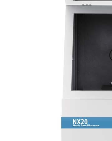
Park NX20 The leading nano metrology tool for failure analysis and large sample research.
|
|
|
- Clifton Tucker
- 5 years ago
- Views:
Transcription


1 The Most Accurate Atomic Force Microscope Park NX20 The leading nano metrology tool for failure analysis and large sample research
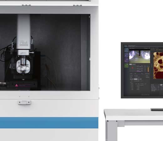
2 The Most Accurate Atomic Force Microscope Park NX20 The premiere choice for failure analysis As an FA engineer, you re expected to deliver results. There s no room for error in the data provided by your instruments. Park NX20, with its reputation as the world s most accurate large sample AFM, is rated so highly in the semiconductor and hard disk industry for its data accuracy. More powerful failure analysis solutions Park NX20 is equipped with unique features that make it easier to uncover the reasons behind device failure and develop more creative solutions. Its unparalleled precision provides high resolution data that lets you focus on your work, while its True Non-Contact mode scan keeps tips sharper and longer, so you won t have to waste as much time and money replacing them. Easy to use, even for entry level engineers Park NX20 has one of the most user friendly designs and automated interfaces in the industry, so you won t have to spend as much time and energy using the tool and supervising junior engineers with the system. This lets you focus your experience on solving bigger problems and providing insightful and timely failure analysis to your customers. Park Systems The Most Accurate Atomic Force Microscope


3


4 Park NX20 Innovative features for innovative work Accurate AFM Solutions for FA and Research Laboratories Surface roughness measurements for media and substrates Defect review imaging and analysis High resolution electrical scan mode Sidewall measurements for 3D structure study Accurate and Reproducible Measurements for Better Productivity Non-contact mode to preserve tip sharpness for surface roughness accuracy Fastest defect imaging in non-contact mode Decoupled XY scanning system for 3D structure measurements Minimized system drift and hysteresis using thermally matched components Accurate AFM Topography with Low Noise Z Detector Sample topography measured by industry leading low noise Z detector True Sample Topography without edge overshoot or piezo creep error Accurate surface height recording, even during high-speed scanning Industry leading forward and backward scan gap of less than 0.15% Cost Savings with True Non-Contact Mode 10 times or longer tip life during general purpose and defect imaging Less tip wear from prolonged high-quality scans Minimized sample damage or modification Park Systems The Most Accurate Atomic Force Microscope

 Piezoelectric creep effect No creep effect No artifact by AFM scanner in low noise closed-loop topography Conventional AFM Park NX")
5 Park NX20 AFM Technology Industry Leading Low Noise Z Detector Our AFMs are equipped with the most effective low noise Z detectors in the field, with a noise of.02 nm over large bandwidth. This produces highly accurate sample topography, no edge overshoot and no need for calibration. Just one of the many ways Park NX20 saves your time and gives you better data. Accurate Sample Topography Measured by Low Noise Z Detector Z Voltage (Topography) Conventional AFM Z Detector (Height) Park NX Series Sample: 1.2 µm Nominal Step Height (9 µm x 1 µm, 2048 pixels x 128 lines) Piezoelectric creep effect No creep effect No artifact by AFM scanner in low noise closed-loop topography Conventional AFM Park NX Series Uses low noise Z detector signal for topography Has low Z detector noise of 0.02 nm over large bandwidth Has no edge overshoot at the leading and trailing edges Needs calibration done only once at the factory Park Systems The Most Accurate Atomic Force Microscope


6 True Non-Contact Mode Preserves Sharp Tip AFM tips are so brittle that touching a sample will instantly reduce the resolution and quality of the image they produce. For soft and delicate samples, the tip will also damage the sample and result in inaccurate sample height measurements, something that can cost you valuable time and money. True Non-Contact mode, a scan mode unique to Park AFMs, consistently produces high resolution and accurate data while maintaining the integrity of the sample. 1:1 aspect ratio Park AFM Before After Taking 20 Images Accurate Feedback by Faster Z-servo enables True Non-Contact AFM Tapping Imaging Tapping Imaging Quick tip wear = Blurred low-resolution scan Destructive tip-sample interaction = Sample damage and modification Highly parameter-dependent True Non-Contact Mode True Non-Contact Mode Less tip wear = Prolonged high-resolution scan Non-destructive tip-sample interaction = Minimized sample modification Immunity from parameter dependent results

 and an ultra fast Z-servo speed of more than 48 mm/sec tip velocity. The maximum Z scan range can be extended from 15 µm to 30 µm with the optional long range Z scanner.")

7 Park NX20 Equipped with the most innovative AFM technology 1 2D Flexure-Guided Scanner with 100 µm x 100 µm Scan Range The XY scanner consists of symmetrical 2-dimensional flexure and high-force piezoelectric stacks provides high orthogonal movement with minimal out-of-plane motion as well as high responsiveness essential for precise sample scanning in the nanometer scale. 2 High Speed Z Scanner with 15 µm Scan Range Driven by a high-force piezoelectric stack and guided by a flexure structure, the standard Z scanner has a high resonant frequency of more than 9 khz (typically 10.5 khz) and an ultra fast Z-servo speed of more than 48 mm/sec tip velocity. The maximum Z scan range can be extended from 15 µm to 30 µm with the optional long range Z scanner. 3 Low Noise XYZ Position Sensors The industry leading low noise Z detector replaces the applied Z voltage as the topography signal while the low noise XY closed loop scan minimizes the forward and backward scan gap to less than 0.15% of the scan range. 4 Motorized XY Sample Stage with Optional Encoders The measurement location of the sample is easily and precisely controlled by the integrated motorized XY stage. The travel range of the XY sample stage can be configured for either 150 mm x 150 mm or 200 mm x 200 mm. The encoders, if used with the motorized stages, enable higher positioning repeatability for accurate sample positioning. The encoded XY stage travels in 1 µm resolution with 2 µm repeatability, and the encoded Z stage, in 0.1 µm resolution with 1 µm repeatability Step-and-Scan Automation 7 Using the motorized sample stage, Step-and-Scan enables programmable multiple region imaging. Here s how it works: Scan an image Lift cantilever Move motorized stage to a user defined coordinate Approach Repeat scan 6 This automated feature greatly increases productivity by reducing the need for your interaction during the scan process. 1 6 Accessible Sample Holder The unique head design can handle up to 200 mm wafer sample size and allows for easy side access to the sample and tip. 5

 allows for a direct on-axis optical view with unprecedented clarity, allowing users to navigate the sample surface easily and find the target area quickly.")

 enables accurate imaging of highly reflective surfaces and precise measurements for pico-newton Force-distance spectroscopy.")
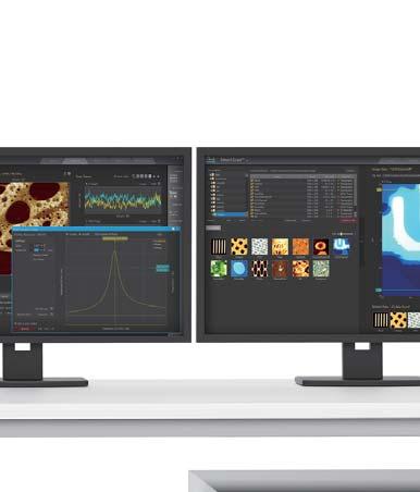
8 7 Expansion Slot for Advanced SPM Modes and Options Advanced SPM modes are easily enabled by plugging an optional module into the expansion slot. And the modular design of the NX-series allows for module compatibility throughout the line. 8 Direct On-Axis High Powered Optics with Integrated LED Illumination The Park NX20 s custom designed objective lens with an ultra long working distance (50 mm, WD 0.21 NA, 1.0 µm resolution) allows for a direct on-axis optical view with unprecedented clarity, allowing users to navigate the sample surface easily and find the target area quickly. With the EL20x objective lens of long travel head, the enlarged sensor size of the CCD provides a resolution of 0.7 µm without compromising visual quality. 9 Auto Engage by Slide-to-Connect SLD Head The AFM head is easily inserted or removed by sliding it along a dovetail rail. This automatically locks the head into its pre-aligned position and connects it to the control electronics with a positioning repeatability of a few microns. The low coherency of the Super Luminescence Diode (SLD) enables accurate imaging of highly reflective surfaces and precise measurements for pico-newton Force-distance spectroscopy. The SLD wavelength eliminates interference issues for users interested in combining the AFM with experiments in the visible spectrum Vertically Aligned Motorized Z Stage and Focus Stage The Z stage and focus stage engage the cantilever with the sample surface while constantly maintaining a clear field of vision for the user. And because the focus stage is motorized and software controlled, it has the precision necessary for transparent samples and liquid cell applications. High Speed 24-bit Digital Electronics 8 All the NX-series AFMs are controlled and processed by the same NX electronics controller. The controller is an all digital, 24-bit high speed electronics which successfully realizes the True Non-Contact mode for accuracy and speed. With its low noise design and high speed processing unit, the controller is also ideal for precise voltage and current measurement as well as nanoscale imaging. The embedded digital signal processing capability adds to the functionality and the economics of our AFM solutions for advanced researchers. 24-bit signal resolution for XY and Z detectors nm resolution in XY (50 µm XY) nm resolution in Z (15 µm Z) 4 3 Embedded digital signal processing capability 3 channels of flexible digital lock-ins Spring constant calibration (thermal method) Digital Q control included Intergrated signal access ports Dedicated and programmable signal input/output ports 7 inputs and 3 outputs

9 Park NX20 Why the world s most accurate large sample AFM is also the easiest to use Easy Tip and Sample Exchange The unique head design allows easy side access allowing you to easily snap new tips and samples into place by hand. The cantilever is ready for scanning without the need for any tricky laser beam alignment by using pre-aligned cantilevers mounted on to the cantilever tip holder. Easy Snap by Hand Closed-loop XY Scan with Dual Servo System for Increased Accuracy The low noise position sensors on each axis of the XY scanner are doubled to attain high scan orthogonality for the largest scan ranges and sample sizes. The secondary sensor corrects and compensates for the non-linear and non-planar positional errors that would occur with a single sensor alone. Dual Servo Sensor Park Systems The Most Accurate Atomic Force Microscope

10 Lightning Fast Automatic Tip Approach Our automatic tip to sample approach requires no user intervention and engages in just 10 seconds after loading the cantilever. By monitoring the cantilever response to the approaching surface, Park NX20 can initiate an automatic fast tip to sample approach within 10 seconds of cantilever loading. Fast feedback by the high speed Z scanner and low noise signal processing by the NX electronics controller enable quick engagement to the sample surface without any user intervention. It just works, minimal user involvement required. Active Temperature Controlled Acoustic Enclosure Designed exclusively for Park NX20, the Acoustic Enclosure is actively temperature-controlled for a perfectly stable thermal environment. The Park NX20 also features active vibration isolation and is completely isolated from external acoustic and light noise so that nothing can interfere with its accuracy. Easy to use controls - Innovative control design allows Park NX20 to quickly reach temperature equilibrium Get scanning faster - Temperature stability of less than 0.05 ºC within 10 minutes of closing the Acoustic Enclosure door W/O Temperature Control Temperature ( C) Drift (µm) Temperature ( C) Drift (µm) Elapsed Time (Hour) Elapsed Time (Hour)

 Piezoelectric Force Microscopy (PFM) Scanning Capacitance Microscopy (SCM) Scanning Kelvin Probe Microscopy (SKPM)")
 Force-Distance (F-d) Spectroscopy Force Volume Imaging Lateral Force Microscopy (LFM)")
 Accurately view your sample s magnetic structure V 0-2.")
 Magnetic domain of High-density HDD media (2 µm x 2 µm)")
11 Park NX20 Power for any project With a wide range of scanning modes and modular design, the Park NX20 has the power and flexibility you need for any project. Surface Roughness Measurement True Non-Contact Mode Dynamic Force Mode Electrical Characterization Conductive AFM (ULCA and VECA) Electric Force Microscopy (EFM) Piezoelectric Force Microscopy (PFM) Scanning Capacitance Microscopy (SCM) Scanning Kelvin Probe Microscopy (SKPM) Scanning Spreading Resistance Microscopy (SSRM) Scanning Tunneling Microscopy (STM) Time-Resolved Photo Current Mapping (Tr-PCM) Mechanical Characterization Force Modulation Microscopy (FMM) Force-Distance (F-d) Spectroscopy Force Volume Imaging Lateral Force Microscopy (LFM) Nanoindentation Nanolithography Phase Imaging Material Property Characterization QuickStep TM SCM The Fastest Scanning Capacitance Microscopy PinPoint TM CP-AFM The Frictionless Conductive Probe AFM Magnetic Force Microscopy (MFM) Accurately view your sample s magnetic structure V µm Defect Site Failure analysis of contact plugs (3 µm x 3 µm) Magnetic domain of High-density HDD media (2 µm x 2 µm) PinPoint TM Nanomechanical Mode, Nanomechanical Property Characterization Topography, Adhesion force, Elastic modulus, Stiffness of Polystyrene-Polybutene Composites are acquired simultaneously in real-time. Topography (10 µm x 10 µm) Adhesion Force (10 µm x 10 µm) Modulus (10 µm x 10 µm)
 The NX20 features Park's automation control software that automatically carries out AFM measurements of a sample according to your")

 The NX20 s innovative architecture")


 Dedicated")
12 Options Customize your AFM to handle any project Automatic data collection and analysis lets you save time Thermal Characterization Scanning Thermal Microscopy (SThM) The NX20 features Park's automation control software that automatically carries out AFM measurements of a sample according to your preset procedure (recipe). It can accurately collect data, perform pattern recognition, and do analysis using its onboard Cognex board and optics module, and export with almost no user input so you have more time to do innovative research. Sample Tilting Stage for Sidewall Imaging lets you see more Magnetic Characterization Magnetic Force Microscopy (MFM) The NX20 s innovative architecture lets you detect the sidewall and surface of the sample, and measure their angle. This gives the unit the versatility you need to do more innovative research and gain deeper insights. Tilting angle: 10, 15, and 20 Sample size: 20 x 20 mm Sample thickness: 2 mm Scanning Thermal Microscopy (SThM) Easily examine your sample s thermal conductivity Our Active Temperature-controlled Acoustic Enclosure lets you take more accurate measurements Innovative control brings the system quickly to its temperature equilibrium Temperature stability of less than 0.05 ºC within10 minutes of closing AE door Includes an active vibration isolation system Encoders for Motorized Stage The encoded XY stage travels in 1 µm resolution with 2 µm repeatability The encoded Z stage travels in 0.1 µm resolution with 1 µm repeatability Sample Plates Temperature map of the Pole-Tip-Recession ofan active hard disk slider (20 µm x 20 µm) Dedicated small sample holder for electrical measurements Vacuum grooves to hold wafers Sample dimension: Up to 200 mm (150 mm default) Clip-type Chip Carrier Can be used with an unmounted cantilever Tip bias function available for Conductive AFM and EFM Tip bias range: -10 V ~ +10 V XY Scanners 20 µm x 20 µm XY Scanner 50 µm x 50 µm XY Scanner 100 µm x 100 µm XY Scanner Z Scanner Heads 15 µm Z Scanner Head 30 µm Z Scanner Head Precise Temperature Control Stiffness (10 µm x 10 µm) Heating & Cooling Stage (0~180 ºC) 250 ºC Heating Stage 600 ºC Heating Stage
13 Park NX20 Specification Scanner XY scanner Single-module flexure XY scanner with closed-loop control Scan range: 100 µm 100 µm 50 µm 50 µm 25 µm 25 µm 20-bit position control and 24-bit position sensor Z scanner Guided high-force Z scanner Scan range: 15 µm 30 µm 20-bit position control and 24-bit position sensor Vision Software Direct on-axis vision of sample surface and cantilever Coupled with 10 objective lens (20 optional) Field-of-view: 840 µm 630 µm CCD: 5 MP NXP Dedicated system control and data acquisition software Adjusting feedback parameters in real time Script-level control through external programs (optional) Objective lens 10 (0.21 NA) objective lens with ultra-long working distance 20 (0.42 NA) objective lens with long working distance and high resolution NXI AFM data analysis software Electronics Signal processing ADC: 18 channels 4 high-speed ADC channels (64 MSPS) 24-bit ADCs for X, Y, and Z scanner position sensor DAC: 12 channels 2 high-speed DAC channels (64 MSPS) 20-bit DACs for X, Y, and Z scanner positioning Maximum data size: 4096 x 4096 pixels Integrated functions 3 channels of flexible digital lock-in amplifier Spring constant calibration (Thermal method) Digital Q control Options/Modes Standard Imaging Electrical Characterization True Non-Contact AFM Basic Contact AFM Lateral Force Microscopy (LFM) Phase Imagin g Intermittent (tapping) AFM Scanning Capacitance Microscopy (SCM) Conductive AFM Electric Force Microscopy (EFM) Piezoresponse Force Microscopy (PFM) Scanning Kelvin Probe Microscopy (SKPM) General Characterization Magnetic Force Microscopy (MFM) Scanning Thermal Microscopy (SThM) F-D Spectroscopy Scanning Tunneling Microscopy (STM) Force Modulation Microscopy (FMM) Nanoindentation Nanolithography Nanomanipulation Options Sample plates Temperature-controlled Acoustic Enclosure Liquid Probehand Liquid Cells Temperature-Controlled Stages External Bias Module Signal Access Module Park Systems The Most Accurate Atomic Force Microscope
14 Stage XY travel range: 150 mm (200 mm optional) Z travel range: 25 mm Focus travel range: 15 mm Precision encoder for all axes (optional) Sample Mount Up to 150 mm (200 mm optional) Vacuum grooves to hold wafer samples External signal access 20 embedded signal input/output ports 5 TTL outputs: EOF, EOL, EOP, Modulation, and AC bias Dimensions in mm 920 mm 820 mm 1450 mm 1280 mm NX20 Atomic Force Microscope 650 mm 850 mm 650 mm


15 Park Systems Dedicated to producing the most accurate and easiest to use AFMs NX E16AB The global headquarters is located at Korean Advanced Nanotechnology Center (KANC) in Suwon, Korea. More than a quarter century ago, the foundations for Park Systems were laid at Stanford University where Dr. Sang-il Park, the founder of Park Systems worked as an integral part of the group that first developed AFM technology. After perfecting the technology, he then went on to create the first commercial AFM and later Park Systems was born. Park Systems strives everyday to live up to the innovative spirit of its beginnings. Throughout our long history, we have honored our commitment to providing the most accurate and yet very easy to use AFMs, with revolutionary features like True Non-Contact mode, and many automated software tools. We are not simply content to rest on our past success. All of our products are designed with same care and creativity that went into our first, allowing you to focus on getting results without worrying about the integrity of your tools.
The Most Accurate Atomic Force Microscope. Park NX20 The leading nano metrology tool for failure analysis and large sample research.
 The Most Accurate Atomic Force Microscope Park NX20 The leading nano metrology tool for failure analysis and large sample research www.parkafm.com Park Systems The Most Accurate Atomic Force Microscope
The Most Accurate Atomic Force Microscope. Park XE15 Power and versatility, brilliantly combined.
 The Most Accurate Atomic Force Microscope Park XE15 Power and versatility, brilliantly combined. www.parkafm.com Park XE15 Increase your productivity with our powerfully versatile atomic force microscope
Park NX10. The most accurate and easiest to use Atomic Force Microscope.
 The most accurate and easiest to use Atomic Force Microscope www.parkafm.com Park Systems Enabling Nanoscale Advances The premiere choice for nanotechnology research Better data Park NX10 produces data
Park XE7 The most affordable research grade AFM with flexible sample handling.
 Park XE7 The most affordable research grade AFM with flexible sample handling www.parkafm.com Park Systems The Most Accurate Atomic Force Microscope Park XE7 The economical choice for innovative research
Park NX-Hivac The world s most accurate and easy to use high vacuum AFM for failure analysis.
 Park NX-Hivac The world s most accurate and easy to use high vacuum AFM for failure analysis www.parkafm.com Park NX-Hivac High vacuum scanning for failure analysis applications 4 x 07 / Cm3 Current (µa)
The World s Most Accurate AFM System. Park NX-3DM Innovation and Efficiency for 3D Metrology.
 The World s Most Accurate AFM System Park NX-3DM Innovation and Efficiency for 3D Metrology www.parkafm.com Park NX-3DM An Indispensable Tool for Wafer Fabrication A fully automated industrial AFM using
INDIAN INSTITUTE OF TECHNOLOGY BOMBAY
 IIT Bombay requests quotations for a high frequency conducting-atomic Force Microscope (c-afm) instrument to be set up as a Central Facility for a wide range of experimental requirements. The instrument
Cutting-edge Atomic Force Microscopy techniques for large and multiple samples
 Cutting-edge Atomic Force Microscopy techniques for large and multiple samples Study of up to 200 mm samples using the widest set of AFM modes Industrial standards of automation A unique combination of
Advanced Nanoscale Metrology with AFM
 Advanced Nanoscale Metrology with AFM Sang-il Park Corp. SPM: the Key to the Nano World Initiated by the invention of STM in 1982. By G. Binnig, H. Rohrer, Ch. Gerber at IBM Zürich. Expanded by the invention
Nanotechnology Solutions Partner
 Nanotechnology Solutions Partner Park Systems Corp. KANC 4F, Iui-Dong 6-10, Suwon, Korea 443-270 Tel. +82-31-546-6800 Fax. +82-31-546-6805 www.parkafm.co.kr Park Systems Inc. 3040 Olcott St. Santa Clara,
SPM The Industry s Performance Leader High Resolution Closed-loop System Fast, Easy Tip & Sample Exchange Versatility and Value Powerful Research
 SPM The Industry s Performance Leader High Resolution Closed-loop System Fast, Easy Tip & Sample Exchange Versatility and Value Powerful Research Flexibility Atomic resolution STM image of highly-oriented
Indian Institute of Technology Bombay
 Specifications for High Resolution Scanning Probe Microscope Item Essential measuring modes with complete hardware and software. All the modes should be demonstrated during installation & training Scanners
Nanosurf easyscan 2 FlexAFM
 Nanosurf easyscan 2 FlexAFM Your Versatile AFM System for Materials and Life Science www.nanosurf.com The new Nanosurf easyscan 2 FlexAFM scan head makes measurements in liquid as simple as measuring in
Outline: Introduction: What is SPM, history STM AFM Image treatment Advanced SPM techniques Applications in semiconductor research and industry
 1 Outline: Introduction: What is SPM, history STM AFM Image treatment Advanced SPM techniques Applications in semiconductor research and industry 2 Back to our solutions: The main problem: How to get nm
Measurement of Microscopic Three-dimensional Profiles with High Accuracy and Simple Operation
 238 Hitachi Review Vol. 65 (2016), No. 7 Featured Articles Measurement of Microscopic Three-dimensional Profiles with High Accuracy and Simple Operation AFM5500M Scanning Probe Microscope Satoshi Hasumura
Lecture 20: Optical Tools for MEMS Imaging
 MECH 466 Microelectromechanical Systems University of Victoria Dept. of Mechanical Engineering Lecture 20: Optical Tools for MEMS Imaging 1 Overview Optical Microscopes Video Microscopes Scanning Electron
- Near Field Scanning Optical Microscopy - Electrostatic Force Microscopy - Magnetic Force Microscopy
 - Near Field Scanning Optical Microscopy - Electrostatic Force Microscopy - Magnetic Force Microscopy Yongho Seo Near-field Photonics Group Leader Wonho Jhe Director School of Physics and Center for Near-field
Nanosurf Nanite. Automated AFM for Industry & Research.
 Nanosurf Nanite Automated AFM for Industry & Research www.nanosurf.com Multiple Measurements Automated Got work? Nanosurf has the solution! The Swiss-based innovator and manufacturer of the most compact
PicoMaster 100. Unprecedented finesse in creating 3D micro structures. UV direct laser writer for maskless lithography
 UV direct laser writer for maskless lithography Unprecedented finesse in creating 3D micro structures Highest resolution in the market utilizing a 405 nm diode laser Structures as small as 300 nm 375 nm
NanoFocus Inc. Next Generation Scanning Probe Technology. Tel : Fax:
 NanoFocus Inc. Next Generation Scanning Probe Technology www.nanofocus.kr Tel : 82-2-864-3955 Fax: 82-2-864-3956 Albatross SPM is Multi functional research grade system Flexure scanner and closed-loop
Keysight Technologies 5500 AFM Controller Upgrade. Data Sheet
 Keysight Technologies 5500 AFM Controller Upgrade Data Sheet 02 Keysight 5500 AFM Controller Upgrade - Data Sheet Upgrade Overview The Keysight 5500 AFM Controller Upgrade offers a tremendously convenient
nanovea.com PROFILOMETERS 3D Non Contact Metrology
 PROFILOMETERS 3D Non Contact Metrology nanovea.com PROFILOMETER INTRO Nanovea 3D Non-Contact Profilometers are designed with leading edge optical pens using superior white light axial chromatism. Nano
Keysight 9500 AFM. Data Sheet
 Keysight 9500 AFM Data Sheet System Overview The Keysight Technologies, Inc. 9500 AFM seamlessly integrates revolutionary new software, a new high-bandwidth digital controller, and a state-of-the-art mechanical
Optical Microscope. Active anti-vibration table. Mechanical Head. Computer and Software. Acoustic/Electrical Shield Enclosure
 Optical Microscope On-axis optical view with max. X magnification Motorized zoom and focus Max Field of view: mm x mm (depends on zoom) Resolution : um Working Distance : mm Magnification : max. X Zoom
PICO MASTER 200. UV direct laser writer for maskless lithography
 PICO MASTER 200 UV direct laser writer for maskless lithography 4PICO B.V. Jan Tinbergenstraat 4b 5491 DC Sint-Oedenrode The Netherlands Tel: +31 413 490708 WWW.4PICO.NL 1. Introduction The PicoMaster
Microscopic Structures
 Microscopic Structures Image Analysis Metal, 3D Image (Red-Green) The microscopic methods range from dark field / bright field microscopy through polarisation- and inverse microscopy to techniques like
Asylum Research. MFP-3D Infinity. Endless Applications. Unlimited Potential. Performance / Versatility / Support
 MFP-3D Infinity AFM Asylum Research Endless Applications. Unlimited Potential. Performance / Versatility / Support MFP-3D Infinity AFM Asylum Research Endless applications. Unlimited potential. The Asylum
10 Things to Consider when Acquiring a Nanopositioning System
 10 Things to Consider when Acquiring a Nanopositioning System There are many factors to consider when looking for nanopositioning piezo stages. This article will help explain some items that are important
LOW TEMPERATURE STM/AFM
 * CreaTec STM of Au(111) using a CO-terminated tip, 20mV bias, 0.6nA* LOW TEMPERATURE STM/AFM High end atomic imaging, spectroscopy and manipulation Designed and manufactured in Germany by CreaTec Fischer
Prepare Sample 3.1. Place Sample in Stage. Replace Probe (optional) Align Laser 3.2. Probe Approach 3.3. Optimize Feedback 3.4. Scan Sample 3.
 Align Laser 3.2. Probe Approach 3.3. Optimize Feedback 3.4. Scan Sample 3.") CHAPTER 3 Measuring AFM Images Learning to operate an AFM well enough to get an image usually takes a few hours of instruction and practice. It takes 5 to 10 minutes to measure an image if the sample is
CHAPTER 3 Measuring AFM Images Learning to operate an AFM well enough to get an image usually takes a few hours of instruction and practice. It takes 5 to 10 minutes to measure an image if the sample is
Manufacturing Metrology Team
 The Team has a range of state-of-the-art equipment for the measurement of surface texture and form. We are happy to discuss potential measurement issues and collaborative research Manufacturing Metrology
Basic methods in imaging of micro and nano structures with atomic force microscopy (AFM)
") Basic methods in imaging of micro and nano P2538000 AFM Theory The basic principle of AFM is very simple. The AFM detects the force interaction between a sample and a very tiny tip (
Basic methods in imaging of micro and nano P2538000 AFM Theory The basic principle of AFM is very simple. The AFM detects the force interaction between a sample and a very tiny tip (
Scanning Microwave. Expanding Impedance Measurements to the Nanoscale: Coupling the Power of Scanning Probe Microscopy with the PNA
 Agilent Technologies Scanning Microwave Microscopy (SMM) Expanding Impedance Measurements to the Nanoscale: Coupling the Power of Scanning Probe Microscopy with the PNA Presented by: Craig Wall PhD Product
Nanonics Systems are the Only SPMs that Allow for On-line Integration with Standard MicroRaman Geometries
 Nanonics Systems are the Only SPMs that Allow for On-line Integration with Standard MicroRaman Geometries 2002 Photonics Circle of Excellence Award PLC Ltd, England, a premier provider of Raman microspectral
Systematic Workflow via Intuitive GUI. Easy operation accomplishes your goals faster than ever.
 Systematic Workflow via Intuitive GUI Easy operation accomplishes your goals faster than ever. 16 With the LEXT OLS4100, observation or measurement begins immediately once the sample is placed on the stage.
Scanning Tunneling Microscopy
 EMSE-515 02 Scanning Tunneling Microscopy EMSE-515 F. Ernst 1 Scanning Tunneling Microscope: Working Principle 2 Scanning Tunneling Microscope: Construction Principle 1 sample 2 sample holder 3 clamps
attosnom I: Topography and Force Images NANOSCOPY APPLICATION NOTE M06 RELATED PRODUCTS G
 APPLICATION NOTE M06 attosnom I: Topography and Force Images Scanning near-field optical microscopy is the outstanding technique to simultaneously measure the topography and the optical contrast of a sample.
Fiber Optic Device Manufacturing
 Precision Motion Control for Fiber Optic Device Manufacturing Aerotech Overview Accuracy Error (µm) 3 2 1 0-1 -2 80-3 40 0-40 Position (mm) -80-80 80 40 0-40 Position (mm) Single-source supplier for precision
Investigate in magnetic micro and nano structures by Magnetic Force Microscopy (MFM)
") Investigate in magnetic micro and nano 5.3.85- Related Topics Magnetic Forces, Magnetic Force Microscopy (MFM), phase contrast imaging, vibration amplitude, resonance shift, force Principle Caution! -
Investigate in magnetic micro and nano 5.3.85- Related Topics Magnetic Forces, Magnetic Force Microscopy (MFM), phase contrast imaging, vibration amplitude, resonance shift, force Principle Caution! -
attocube systems Probe Stations for Extreme Environments CRYOGENIC PROBE STATION fundamentals principles of cryogenic probe stations
 PAGE 88 & 2008 2007 PRODUCT CATALOG CRYOGENIC PROBE STATION fundamentals...................... 90 principles of cryogenic probe stations attocps I.......................... 92 ultra stable cryogenic probe
SENSOR+TEST Conference SENSOR 2009 Proceedings II
 B8.4 Optical 3D Measurement of Micro Structures Ettemeyer, Andreas; Marxer, Michael; Keferstein, Claus NTB Interstaatliche Hochschule für Technik Buchs Werdenbergstr. 4, 8471 Buchs, Switzerland Introduction
MEMS for RF, Micro Optics and Scanning Probe Nanotechnology Applications
 MEMS for RF, Micro Optics and Scanning Probe Nanotechnology Applications Part I: RF Applications Introductions and Motivations What are RF MEMS? Example Devices RFIC RFIC consists of Active components
Options and Accessories for Asylum Research MFP-3D AFMs
 ACCESSORIES Options and Accessories for Asylum Research MFP-3D AFMs Empower your research with powerful, innovative new capabilities Go beyond topography with advanced modes and environmental control Powerful
Ionscope SICM. About Ionscope. Scanning Ion Conductance Microscopy. Ionscope A brand of Openiolabs Limited
 SICM About is a brand of openiolabs Ltd, headquartered in Cambridge UK, is the world-leader in (SICM), a rapidly emerging Scanning Probe Microscopy (SPM) technique which allows nanoscale topographical
ATOMIC FORCE MICROSCOPY
 B47 Physikalisches Praktikum für Fortgeschrittene Supervision: Prof. Dr. Sabine Maier sabine.maier@physik.uni-erlangen.de ATOMIC FORCE MICROSCOPY Version: E1.4 first edit: 15/09/2015 last edit: 05/10/2018
Atomic Force Microscopy (Bruker MultiMode Nanoscope IIIA)
") Atomic Force Microscopy (Bruker MultiMode Nanoscope IIIA) This operating procedure intends to provide guidance for general measurements with the AFM. For more advanced measurements or measurements with
Atomic Force Microscopy (Bruker MultiMode Nanoscope IIIA) This operating procedure intends to provide guidance for general measurements with the AFM. For more advanced measurements or measurements with
Nanoscale Material Characterization with Differential Interferometric Atomic Force Microscopy
 Nanoscale Material Characterization with Differential Interferometric Atomic Force Microscopy F. Sarioglu, M. Liu, K. Vijayraghavan, A. Gellineau, O. Solgaard E. L. Ginzton Laboratory University Tip-sample
OPTICS IN MOTION. Introduction: Competing Technologies: 1 of 6 3/18/2012 6:27 PM.
 1 of 6 3/18/2012 6:27 PM OPTICS IN MOTION STANDARD AND CUSTOM FAST STEERING MIRRORS Home Products Contact Tutorial Navigate Our Site 1) Laser Beam Stabilization to design and build a custom 3.5 x 5 inch,
attocfm I for Surface Quality Inspection NANOSCOPY APPLICATION NOTE M01 RELATED PRODUCTS G
 APPLICATION NOTE M01 attocfm I for Surface Quality Inspection Confocal microscopes work by scanning a tiny light spot on a sample and by measuring the scattered light in the illuminated volume. First,
Figure for the aim4np Report
 Figure for the aim4np Report This file contains the figures to which reference is made in the text submitted to SESAM. There is one page per figure. At the beginning of the document, there is the front-page
; A=4π(2m) 1/2 /h. exp (Fowler Nordheim Eq.) 2 const
 1/2 /h. exp (Fowler Nordheim Eq.) 2 const") Scanning Tunneling Microscopy (STM) Brief background: In 1981, G. Binnig, H. Rohrer, Ch. Gerber and J. Weibel observed vacuum tunneling of electrons between a sharp tip and a platinum surface. The tunnel
Scanning Tunneling Microscopy (STM) Brief background: In 1981, G. Binnig, H. Rohrer, Ch. Gerber and J. Weibel observed vacuum tunneling of electrons between a sharp tip and a platinum surface. The tunnel
Using Nanoelectrical Solutions to expand the capability of AFM Dr. Peter De Wolf
 Using Nanoelectrical Solutions to expand the capability of AFM Dr. Peter De Wolf peter.dewolf@bruker.com 2 Atomic Force Microscopy (AFM) Microscopy technique based on raster-scanning and small tipsample
P-611.Z Piezo Z-Stage
 Physik Instrumente (PI) GmbH & Co. KG 2008. Subject to change without notice. All data are superseded by any new release. The newest release for data sheets is available for download at www.pi.ws. Cat120E
Introduction of New Products
 Field Emission Electron Microscope JEM-3100F For evaluation of materials in the fields of nanoscience and nanomaterials science, TEM is required to provide resolution and analytical capabilities that can
queensgate a brand of Elektron Technology
 NanoSensors NX/NZ NanoSensor The NanoSensor is a non-contact position measuring system based on the principle of capacitance micrometry. Two sensor plates, a Target and a Probe, form a parallel plate capacitor.
Compact Nanopositioning System Family with Long Travel Ranges
 P-620.1 P-629.1 PIHera Piezo Linear Stage Compact Nanopositioning System Family with Long Travel Ranges Physik Instrumente (PI) GmbH & Co. KG 2008. Subject to change without notice. All data are superseded
Standard Operating Procedure of Atomic Force Microscope (Anasys afm+)
") Standard Operating Procedure of Atomic Force Microscope (Anasys afm+) The Anasys Instruments afm+ system incorporates an Atomic Force Microscope which can scan the sample in the contact mode and generate
Standard Operating Procedure of Atomic Force Microscope (Anasys afm+) The Anasys Instruments afm+ system incorporates an Atomic Force Microscope which can scan the sample in the contact mode and generate
Ion Beam Lithography next generation nanofabrication
 Ion Beam Lithography next generation nanofabrication EFUG Bordeaux 2011 ion beams develop Lloyd Peto IBL sales manager Copyright 2011 by Raith GmbH ionline new capabilities You can now Apply an ion beam
contents TABLE OF The SECOM platform Applications - sections Applications - whole cells Features Integrated workflow Automated overlay
 S E C O M TABLE OF contents The SECOM platform 4 Applications - sections 5 Applications - whole cells 8 Features 9 Integrated workflow 12 Automated overlay ODEMIS - integrated software Specifications 13
Agilent Technologies Scanning Probe Microscope. User s Guide. Agilent Technologies
 Agilent Technologies 5500 Scanning Probe Microscope User s Guide Agilent Technologies Notices Agilent Technologies, Inc. 2008 No part of this manual may be reproduced in any form or by any means (including
Motion Solutions for Digital Pathology
 Parker Hannifin Electromechanical Dvision N. A. 1140 Sandy Hill Road Irwin, PA 1564203049 724-861-8200 www.parkermotion.com Motion Solutions for Digital Pathology By: Brian Handerhan and Jim Monnich Design
UNIVERSITY OF WATERLOO Physics 360/460 Experiment #2 ATOMIC FORCE MICROSCOPY
 UNIVERSITY OF WATERLOO Physics 360/460 Experiment #2 ATOMIC FORCE MICROSCOPY References: http://virlab.virginia.edu/vl/home.htm (University of Virginia virtual lab. Click on the AFM link) An atomic force
Bringing Answers to the Surface
 3D Bringing Answers to the Surface 1 Expanding the Boundaries of Laser Microscopy Measurements and images you can count on. Every time. LEXT OLS4100 Widely used in quality control, research, and development
Comparison of resolution specifications for micro- and nanometer measurement techniques
 P4.5 Comparison of resolution specifications for micro- and nanometer measurement techniques Weckenmann/Albert, Tan/Özgür, Shaw/Laura, Zschiegner/Nils Chair Quality Management and Manufacturing Metrology
M-041 M-044 Tip/Tilt Stage
 M-041 M-044 Tip/Tilt Stage Piezo Drive Option for Nanometer Precision Ordering Information Linear Actuators & Motors M-041.00 Small Tilt Stage, Manual Micrometer Drive M-041.D01 Small Tilt Stage, DC-Motor
Rebirth of Force Spectroscopy: Advanced Nanomechanical, Electrical, Optical, Thermal and Piezoresponse Studies
 HybriD Mode Rebirth of Force Spectroscopy: Advanced Nanomechanical, Electrical, Optical, Thermal and Piezoresponse Studies Fast Quantitative Nanomechanical Measurements and Force Volume Simultaneous Electrostatic
Nmark AGV-HP. High Accuracy, Thermally Stable Galvo Scanner
 Nmark AGV-HP High Accuracy, Thermally Stable Galvo Scanner Highest accuracy scanner available attains single-digit, micron-level accuracy over the field of view Optical feedback technology significantly
Atomic Force Microscopes
 Nanoscale Surface Characterization tomic Force Microscopes www.witec.de WITec tomic Force Microscopes Nanoscale Surface Characterization The WITec tomic Force Microscope (FM) module integrated with a research-grade
taccor Optional features Overview Turn-key GHz femtosecond laser
 taccor Turn-key GHz femtosecond laser Self-locking and maintaining Stable and robust True hands off turn-key system Wavelength tunable Integrated pump laser Overview The taccor is a unique turn-key femtosecond
Micro-manipulated Cryogenic & Vacuum Probe Systems
 Janis micro-manipulated probe stations are designed for non-destructive electrical testing using DC, RF, and fiber-optic probes. They are useful in a variety of fields including semiconductors, MEMS, superconductivity,
Fast Optical Form Measurements of Rough Cylindrical and Conical Surfaces in Diesel Fuel Injection Components
 Fast Optical Form Measurements of Rough Cylindrical and Conical Surfaces in Diesel Fuel Injection Components Thomas J. Dunn, Robert Michaels, Simon Lee, Mark Tronolone, and Andrew Kulawiec; Corning Tropel
The NanomechPro Toolkit: Accurate Tools for Measuring Nanoscale Mechanical Properties for Diverse Materials
 NanomechPro Toolkit DATA SHEET 43 The NanomechPro Toolkit: Accurate Tools for Measuring Nanoscale Mechanical Properties for Diverse Materials Understanding nanoscale mechanical properties is of fundamental
Motion Solutions for Digital Pathology. White Paper
 Motion Solutions for Digital Pathology White Paper Design Considerations for Digital Pathology Instruments With an ever increasing demand on throughput, pathology scanning applications are some of the
Optical Characterization and Defect Inspection for 3D Stacked IC Technology
 Minapad 2014, May 21 22th, Grenoble; France Optical Characterization and Defect Inspection for 3D Stacked IC Technology J.Ph.Piel, G.Fresquet, S.Perrot, Y.Randle, D.Lebellego, S.Petitgrand, G.Ribette FOGALE
Nmark AGV-HP. High Accuracy, Thermally Stable Galvo Scanner
 Nmark AGV-HP Galvanometer Nmark AGV-HP High Accuracy, Thermally Stable Galvo Scanner Highest accuracy scanner available attains single-digit, micron-level accuracy over the field of view Optical feedback
MPI TS300-SE 300 mm Manual Probe System with ShielDEnvironment TM For accurate and reliable DC/CV, RF and mmw measurements
 MPI TS300-SE 300 mm Manual Probe System with ShielDEnvironment TM For accurate and reliable DC/CV, RF and mmw measurements FEATURES / BENEFITS Universal Use Designed for wide variety of applications such
PICO MASTER. UV direct laser writer for maskless lithography
 4PICO B.V. Jan Tinbergenstraat 4b 5491 DC Sint-Oedenrode The Netherlands Tel: +31 413 490708 PICO MASTER UV direct laser writer for maskless lithography Introduction The PicoMaster is a versatile UV laser
FemtoFAB. Femtosecond laser micromachining system. tel fax Konstitucijos ave. 23C LT Vilnius, Lithuania
 FemtoFAB Femtosecond laser micromachining system Konstitucijos ave. 23C LT-08105 Vilnius, Lithuania tel. +370 5 272 57 38 fax +370 5 272 37 04 info@wophotonics.com www.wophotonics.com INTRODUCTION FemtoFAB
University of MN, Minnesota Nano Center Standard Operating Procedure
 Equipment Name: Atomic Force Microscope Badger name: afm DI5000 PAN Revisionist Paul Kimani Model: Dimension 5000 Date: October 6, 2017 Location: Bay 1 PAN Revision: 1 A. Description i. Enhanced Motorized
Electric polarization properties of single bacteria measured with electrostatic force microscopy
 Electric polarization properties of single bacteria measured with electrostatic force microscopy Theoretical and practical studies of Dielectric constant of single bacteria and smaller elements Daniel
Lateral Force: F L = k L * x
 Scanning Force Microscopy (SFM): Conventional SFM Application: Topography measurements Force: F N = k N * k N Ppring constant: Spring deflection: Pieo Scanner Interaction or force dampening field Contact
Surface Finish Measurement Methods and Instrumentation
 125 years of innovation Surface Finish Measurement Methods and Instrumentation Contents Visual Inspection Surface Finish Comparison Plates Contact Gauges Inductive / Variable Reluctance (INTRA) Piezo Electric
Zeta-300 3D OPTICAL PROFILER
 Zeta-300 3D OPTICAL PROFILER Technology Toolkit Developed in 2007, the revolutionary Confocal Grid Structured Illumination (CGSI) is the powerful technology in all Zeta Optical Profilers but in a Zeta,
Description of options, upgrades and accessories for the laser beam stabilization system Compact
 Description of options, upgrades and accessories for the laser beam stabilization system Compact The basic configuration of the Compact laser beam stabilization system is fully equipped for stabilization
Akiyama-Probe (A-Probe) guide
 guide") Akiyama-Probe (A-Probe) guide This guide presents: what is Akiyama-Probe, how it works, and what you can do Dynamic mode AFM Version: 2.0 Introduction NANOSENSORS Akiyama-Probe (A-Probe) is a self-sensing
Akiyama-Probe (A-Probe) guide This guide presents: what is Akiyama-Probe, how it works, and what you can do Dynamic mode AFM Version: 2.0 Introduction NANOSENSORS Akiyama-Probe (A-Probe) is a self-sensing
Advanced 3D Optical Profiler using Grasshopper3 USB3 Vision camera
 Advanced 3D Optical Profiler using Grasshopper3 USB3 Vision camera Figure 1. The Zeta-20 uses the Grasshopper3 and produces true color 3D optical images with multi mode optics technology 3D optical profiling
Flex-Axiom. Nanosurf. The Most Versatile AFM System for Materials Research
 Flex-Axiom The Most Versatile AFM System for Materials Research Measurement capabilities in air and liquid Versatility in applications and Compatibility with inverted microscopes High precision scanning
Standard Operating Procedure
 Standard Operating Procedure Nanosurf Atomic Force Microscopy Operation Facility NCCRD Nanotechnology Center for Collaborative Research and Development Department of Chemistry and Engineering Physics The
Super High Vertical Resolution Non-Contact 3D Surface Profiler BW-S500/BW-D500 Series
 Super High Vertical Resolution Non-Contact 3D Surface Profiler BW-S500/BW-D500 Series Nikon's proprietary scanning-type optical interference measurement technology achieves 1pm* height resolution. * Height
Application Note #548 AcuityXR Technology Significantly Enhances Lateral Resolution of White-Light Optical Profilers
 Application Note #548 AcuityXR Technology Significantly Enhances Lateral Resolution of White-Light Optical Profilers ContourGT with AcuityXR TM capability White light interferometry is firmly established
Improving the Collection Efficiency of Raman Scattering
 PERFORMANCE Unparalleled signal-to-noise ratio with diffraction-limited spectral and imaging resolution Deep-cooled CCD with excelon sensor technology Aberration-free optical design for uniform high resolution
Fastest high definition Raman imaging. Fastest Laser Raman Microscope RAMAN
 Fastest high definition Raman imaging Fastest Laser Raman Microscope RAMAN - 11 www.nanophoton.jp Observation A New Generation in Raman Observation RAMAN-11 developed by Nanophoton was newly created by
ezafm OPERATING MANUAL
 ezafm OPERATING MANUAL 2013rev 2.0 1 Table of Contents CHAPTER 1:ezAFM... 4 1.1. Introduction... 5 1.2. System Components... 5 1.3. Unpacking and Packing the Instrument... 6 1.3.1. Before Installation...
Bruker Dimension Icon AFM Quick User s Guide
 Bruker Dimension Icon AFM Quick User s Guide March 3, 2015 GLA Contacts Jingjing Jiang (jjiang2@caltech.edu 626-616-6357) Xinghao Zhou (xzzhou@caltech.edu 626-375-0855) Bruker Tech Support (AFMSupport@bruker-nano.com
Instructions for the Experiment
 Instructions for the Experiment Excitonic States in Atomically Thin Semiconductors 1. Introduction Alongside with electrical measurements, optical measurements are an indispensable tool for the study of
OPTOFORM 40 ENGINEERING SPECIFICATIONS
 OPTOFORM 40 The world s most competitively priced Ultra Precision Lathe specifically designed for manufacturing both INTRA-OCULAR LENSES and CONTACT LENSES. ENGINEERING SPECIFICATIONS Description Through
Nmark AGV-HPO. High Accuracy, Open Frame, Thermally Stable Galvo Scanner. Highest accuracy scanner available attains singledigit,
 Nmark AGV-HPO Galvanometer Nmark AGV-HPO High Accuracy, Open Frame, Thermally Stable Galvo Scanner Highest accuracy scanner available attains singledigit, micron-level accuracy over the field of view Optical
Unit-25 Scanning Tunneling Microscope (STM)
") Unit-5 Scanning Tunneling Microscope (STM) Objective: Imaging formation of scanning tunneling microscope (STM) is due to tunneling effect of quantum physics, which is in nano scale. This experiment shows
Unit-5 Scanning Tunneling Microscope (STM) Objective: Imaging formation of scanning tunneling microscope (STM) is due to tunneling effect of quantum physics, which is in nano scale. This experiment shows
PSD Characteristics. Position Sensing Detectors
 PSD Characteristics Position Sensing Detectors Silicon photodetectors are commonly used for light power measurements in a wide range of applications such as bar-code readers, laser printers, medical imaging,
CONSTRUCTING A SCANNING TUNNELING MICROSCOPE FOR THE STUDY OF SUPERCONDUCTIVITY
 CONSTRUCTING A SCANNING TUNNELING MICROSCOPE FOR THE STUDY OF SUPERCONDUCTIVITY CHRISTOPHER STEINER 2012 NSF/REU Program Physics Department, University of Notre Dame Advisors: DR. MORTEN ESKILDSEN CORNELIUS