PH880 Topics in Physics
|
|
|
- Brice Taylor
- 6 years ago
- Views:
Transcription
1 PH880 Topics in Physics Modern Optical Imaging (Fall 2010)
2 Overview of week 12 Monday: FRET Wednesday: NSOM
3 Förster resonance energy transfer (FRET) Fluorescence emission i FRET Donor Acceptor wikipedia
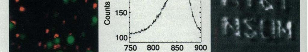
4 FRET: spectroscopic ruler Determines distances between biomolecules labeled with an appropriate donor and acceptor fluorochrome when they are within 10 nanometers of each other. (* normal diffraction limited it d fluorescence microscope resolution is insufficient i to determine whether an interaction between biomolecules actually takes place.) Teakjip Ha group
5 508 VOL.5 NO.6 JUNE 2008 NATURE METHODS
6 Overview of week 12 Monday: FRET Wednesday: NSOM


")


7 Things Natural The Scale of Things Nanometers and More 10-2 m 1 cm 10 mm Things Manmade Head of a pin 1-2 mm The Challenge Ant ~ m mm Dust mite 200 mm 10-4 m 0.1 mm 100 mm 1,000,000 nanometers = 1 millimeter (mm) e Microwave MicroElectroMechanic al (MEMS) devices mm wide Human hair ~ mm wide Red blood cells (~7-8 mm) ~10 nm diameter Fly ash ~ mm ATP synthase Microworld Nan noworld 10-5 m 10-6 m 10-7 m 10-8 m Infrared Visible Ultraviolet 0.01 mm 10 mm mm 100 nm Pollen grain Red blood cells 1,000 nanometers = Zone plate x-ray lens 1 micrometer Outer ring spacing ~35 nm (mm) 0.01 mm 10 nm Self-assembled, Nature-inspired structure Many 10s of nm Nanotube electrode O O S O O O O O O O O O O O S O S O S Fabricate and combine nanoscale building blocks to make useful devices, e.g., a photosynthetic reaction center with integral semiconductor storage. O S P O O O O S O O S O S DNA ~2-1/2 nm diameter Atoms of silicon spacing nm 10-9 m m Soft x-r ray 1 nanometer (nm) 0.1 nm Quantum corral of 48 iron atoms on copper surface positioned one at a time with an STM tip Corral diameter 14 nm Carbon buckyball ~1 nm Carbon nanotube diameter ~1.3 nm diameter Office of Basic Energy Science Office of Science, U.S. DOE Version , pmd
8 Scanning probe microscopes Scanning Tunneling Microscope STM Atomic Force Microscope AFM Nearfield Scanning Optical Microscope NSOM
9 Scanning Tunneling Microscope: STM Binnig and Rohrer won Nobel Prize in 1986 for the development of STM S. Woedtke, Ph.D. thesis, Inst.f.Exp.u.Ang.Phys. der CAU Kiel, When STM tip is close to the specimen (~ 1nm), a tunneling current, I T is established I T is exponentially proportional to the distance A feedback loop maintaining I T can change z position topographical p information


10 STM images "quantum corral" Atom Carbon Monoxide Man Iron on Copper Iron on Copper Carbon Monoxide on Platinum Don Eigler, IBM Lutz & Eigler, IBM Lutz & Eigler, IBM


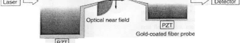
11 Atomic Force Microscope AFM STM is a precursor of AFM Feedback Loop V Laser PZT Mirror Photodiode ~ deflection Tip ThermoMicroscopes Explorer AFM Substrate AFM relies on contact rather than current nonconductive materials can be imaged


12 AFM images the compaction of DNA in yeast caused by a protein ti called AbF2 nuclear pore complex LR Brewer, et al, Biophysical journal, 2003 D Stoffler et al, Current opinion in cell biology, 1999
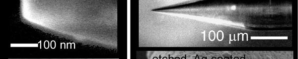
13 AFM + Fluorescence imaging techniques A. Gaiduk et al, Chem. Phys. Chem. 6, no. 5, pp , 2005

14 Near field
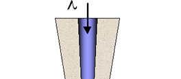
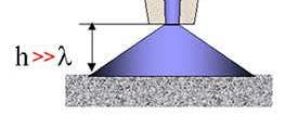
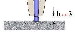
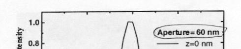
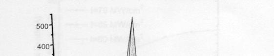
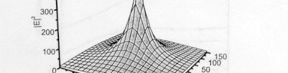
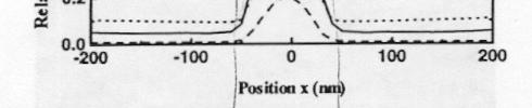
15 sub wavelength aperture (a) ( nm) ~10 nm Image can be reconstructed point by point spatial resolution is limited by a (rather than λ)
16 the propagation of waves :the loss of spatialinformationinformation Hartschuh et al., Angewandte Chemie,2008
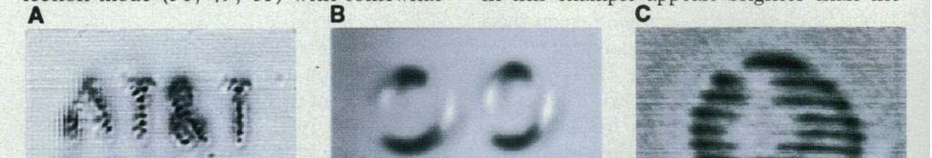
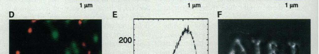
17 History of NSOM 1. Theoretically proposed in 1928, EH Synge, Philos. Mag. 6, 356 (1928) 2. Demonstration at microwave frequencies with a resolution of λ/60. EA Ash ad G. Nicholls, Nature (London) 237, 510 (1972) 3. At visible wavelengths ( optical stethoscopy ) was demonstrated. D. Pohl, W. Denk, and M. Lanz, Appl. Phys. Lett. 44, 651 (1984) 4. Betzig et al used fiber probes to image a variety of samples with a number of different contrast mechanisms. Betzig, E. & Trautman, JK Science 257
18
19
20
 Micro fabrication Fast Large cone")
 Toxic (HF) vapor Difficult")
 Fragile Complex fabrication")
21 NSOM tip fabrication chemical etching (meniscus or tube etching) Micro fabrication Fast Large cone angle Fast, convenient process mass production. (Low cost, reproducible) Toxic (HF) vapor Difficult to control surface quality Smooth surface Low cone angle (low throughput) Fragile Complex fabrication process


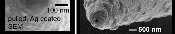
22 NSOM tip: metal coating
23 NSOM tip: illumination Waveguide tip (Takashi et al.1999) SiO2 cantilevered tip (Mitsuoka et al. 2000) Fiber tip by Nanonics Inc.


24 NSOM tip: intensity distribution Probe to Probe configuration (Ohtsu et al. 2000) Minh et al Lu et al. 2001
25 NSOM tip: geometry and light throughput Ultramicroscopy 57 (1995)
26 Common NSOM illumination
27 Other focusing concepts using near field optics Hartschuh et al., Angewandte Chemie,2008 a) Far field focusing using a lens. The angular frequency range of propagating p gwaves kx,max, and thus the focus diameter, is limited by the aperture angle of the lens kx,max=nsin(q)2p/l, with n being the refractive index and l the wavelength of light. b) Aperture type scanning near field optical microscope (aperture SNOM). c) Tip enhanced near field optical microscopy (TENOM). d) Tip on aperture (TOA) approach, which combines the advantages of (b) and (c).
28 Oscillatory Feedback Methods Oscillating ~ 1 nm at resonance freq (~ 30 khz) Increases SNR for feedback methods Q factor ~ 500 (the oscillator's resonance frequency divided by its resonance width) 1. Shear force detection utilizes lateral oscillation shear forces generated between the tip andspecimen (parallel to the surface) to control the tipspecimen gap during imaging 2. Tapping mode detection relies on atomic forces occurring during oscillation of the tip perpendicular to the specimen surface (as in AFM) to generate the feedback signal for tip control.
29 Reading List BetzigE, Lewis A, Harootunian A, Isaacson M, & Kratschmer E (1986) Near Field ildscanning Optical Microscopy (NSOM): Development and Biophysical Applications. Biophys J 49(1):
NSOM (SNOM) Overview
 Overview") NSOM (SNOM) Overview The limits of far field imaging In the early 1870s, Ernst Abbe formulated a rigorous criterion for being able to resolve two objects in a light microscope: d > ë / (2sinè) where d
NSOM (SNOM) Overview The limits of far field imaging In the early 1870s, Ernst Abbe formulated a rigorous criterion for being able to resolve two objects in a light microscope: d > ë / (2sinè) where d
Nanotechnology, the infrastructure, and IBM s research projects
 Nanotechnology, the infrastructure, and IBM s research projects Dr. Paul Seidler Coordinator Nanotechnology Center, IBM Research - Zurich Nanotechnology is the understanding and control of matter at dimensions
Nano Scale Optics with Nearfield Scanning Optical Microscopy (NSOM)
") Nano Scale Optics with Nearfield Scanning Optical Microscopy (NSOM) Presentation Overview Motivation for nearfield optics Introduction to NSOM What is NSOM today? What can you do with NSOM? November 2,
Nano Scale Optics with Nearfield Scanning Optical Microscopy (NSOM) Presentation Overview Motivation for nearfield optics Introduction to NSOM What is NSOM today? What can you do with NSOM? November 2,
Study of shear force as a distance regulation mechanism for scanning near-field optical microscopy
 Study of shear force as a distance regulation mechanism for scanning near-field optical microscopy C. Durkan a) and I. V. Shvets Department of Physics, Trinity College Dublin, Ireland Received 31 May 1995;
Lecture 20: Optical Tools for MEMS Imaging
 MECH 466 Microelectromechanical Systems University of Victoria Dept. of Mechanical Engineering Lecture 20: Optical Tools for MEMS Imaging 1 Overview Optical Microscopes Video Microscopes Scanning Electron
- Near Field Scanning Optical Microscopy - Electrostatic Force Microscopy - Magnetic Force Microscopy
 - Near Field Scanning Optical Microscopy - Electrostatic Force Microscopy - Magnetic Force Microscopy Yongho Seo Near-field Photonics Group Leader Wonho Jhe Director School of Physics and Center for Near-field
attosnom I: Topography and Force Images NANOSCOPY APPLICATION NOTE M06 RELATED PRODUCTS G
 APPLICATION NOTE M06 attosnom I: Topography and Force Images Scanning near-field optical microscopy is the outstanding technique to simultaneously measure the topography and the optical contrast of a sample.
Fabrication of Probes for High Resolution Optical Microscopy
 Fabrication of Probes for High Resolution Optical Microscopy Physics 564 Applied Optics Professor Andrès La Rosa David Logan May 27, 2010 Abstract Near Field Scanning Optical Microscopy (NSOM) is a technique
International Journal of Nano Dimension
 ISSN: 2008-8868 Contents list available at IJND International Journal of Nano Dimension Journal homepage: www.ijnd.ir Review article An overview of scanning near-field optical microscopy in characterization
Microscopic Structures
 Microscopic Structures Image Analysis Metal, 3D Image (Red-Green) The microscopic methods range from dark field / bright field microscopy through polarisation- and inverse microscopy to techniques like
Near-field Optical Microscopy
 Near-field Optical Microscopy R. Fernandez, X. Wang, N. Li, K. Parker, and A. La Rosa Physics Department Portland State University Portland, Oregon Near-Field SPIE Optics Microscopy East 2005 Group PSU
; A=4π(2m) 1/2 /h. exp (Fowler Nordheim Eq.) 2 const
 1/2 /h. exp (Fowler Nordheim Eq.) 2 const") Scanning Tunneling Microscopy (STM) Brief background: In 1981, G. Binnig, H. Rohrer, Ch. Gerber and J. Weibel observed vacuum tunneling of electrons between a sharp tip and a platinum surface. The tunnel
Scanning Tunneling Microscopy (STM) Brief background: In 1981, G. Binnig, H. Rohrer, Ch. Gerber and J. Weibel observed vacuum tunneling of electrons between a sharp tip and a platinum surface. The tunnel
Spectroscopic infrared scanning near-field optical microscopy (IR-SNOM)
") Journal of Alloys and Compounds 401 (2005) 80 85 Spectroscopic infrared scanning near-field optical microscopy (IR-SNOM) D. Vobornik a,, G. Margaritondo a, J.S. Sanghera b, P. Thielen b,i.d.aggarwal b,
Journal of Alloys and Compounds 401 (2005) 80 85 Spectroscopic infrared scanning near-field optical microscopy (IR-SNOM) D. Vobornik a,, G. Margaritondo a, J.S. Sanghera b, P. Thielen b,i.d.aggarwal b,
MEMS for RF, Micro Optics and Scanning Probe Nanotechnology Applications
 MEMS for RF, Micro Optics and Scanning Probe Nanotechnology Applications Part I: RF Applications Introductions and Motivations What are RF MEMS? Example Devices RFIC RFIC consists of Active components
Investigation of the Near-field Distribution at Novel Nanometric Aperture Laser
 Investigation of the Near-field Distribution at Novel Nanometric Aperture Laser Tiejun Xu, Jia Wang, Liqun Sun, Jiying Xu, Qian Tian Presented at the th International Conference on Electronic Materials
Applications of Optics
 Nicholas J. Giordano www.cengage.com/physics/giordano Chapter 26 Applications of Optics Marilyn Akins, PhD Broome Community College Applications of Optics Many devices are based on the principles of optics
Evaluation of Transducers with Near-field Scanning of Their Sl~rfaces
 Evaluation of Transducers with Near-field Scanning of Their Sl~rfaces Jian-yu Ln and James F. Greenleaf Biodynamics Research Unit. Department of Physiology and Biophysics, Mayo Clinic and Foundation. Rochester,
Nanonics Systems are the Only SPMs that Allow for On-line Integration with Standard MicroRaman Geometries
 Nanonics Systems are the Only SPMs that Allow for On-line Integration with Standard MicroRaman Geometries 2002 Photonics Circle of Excellence Award PLC Ltd, England, a premier provider of Raman microspectral
Beams and Scanning Probe Microscopy
 IFN-CNR, Sezione di Trento Istituto Trentino di Cultura of Trento Department of Physics University of Trento Towards the joint use of X-ray Beams and Scanning Probe Microscopy Silvia Larcheri SILS 2005
RECENTLY, using near-field scanning optical
 1 2 1 2 Theoretical and Experimental Study of Near-Field Beam Properties of High Power Laser Diodes W. D. Herzog, G. Ulu, B. B. Goldberg, and G. H. Vander Rhodes, M. S. Ünlü L. Brovelli, C. Harder Abstract
Outline: Introduction: What is SPM, history STM AFM Image treatment Advanced SPM techniques Applications in semiconductor research and industry
 1 Outline: Introduction: What is SPM, history STM AFM Image treatment Advanced SPM techniques Applications in semiconductor research and industry 2 Back to our solutions: The main problem: How to get nm
Diffraction, Fourier Optics and Imaging
 1 Diffraction, Fourier Optics and Imaging 1.1 INTRODUCTION When wave fields pass through obstacles, their behavior cannot be simply described in terms of rays. For example, when a plane wave passes through
Advanced Nanoscale Metrology with AFM
 Advanced Nanoscale Metrology with AFM Sang-il Park Corp. SPM: the Key to the Nano World Initiated by the invention of STM in 1982. By G. Binnig, H. Rohrer, Ch. Gerber at IBM Zürich. Expanded by the invention
Microscopy Techniques that make it easy to see things this small.
 Microscopy Techniques that make it easy to see things this small. What is a Microscope? An instrument for viewing objects that are too small to be seen easily by the naked eye. Dutch spectacle-makers Hans
3D simulations of the experimental signal measured in near-field optical microscopy
 Journal of Microscopy, Vol. 194, Pt 2/3, May/June 1999, pp. 235 239. Received 6 December 1998; accepted 4 February 1999 3D simulations of the experimental signal measured in near-field optical microscopy
Department of Physics, Dalian University of Technology, Dalian
 Solid State Phenomena Online: 2007-03-15 ISSN: 1662-9779, Vols. 121-123, pp 689-692 doi:10.4028/www.scientific.net/ssp.121-123.689 2007 Trans Tech Publications, Switzerland Fabrication of a brush-shaped
Table 1: Drive efficiency of the SNOM probe as indicated by the ratio between the drive amplitude and the amplitude of the cantilever tunes
 Fabrication of optical fiber probes for scanning near-field optical microscopy Si Yue Guo*, Jeffrey M. LeDue, Peter Grütter Department of Physics, McGill University, 3600 University, Montreal, Canada,
Near-field optics: from subwavelength illumination to nanometric shadowing
 FOCUS ON OPTICAL IMAGING Near-field optics: from subwavelength illumination to nanometric shadowing Aaron Lewis, Hesham Taha, Alina Strinkovski, Alexandra Manevitch, Artium Khatchatouriants, Rima Dekhter
Near Field Optical Microscopy Characterization of IC Metrology
 Rochester Institute of Technology RIT Scholar Works Presentations and other scholarship 5-1-1994 Near Field Optical Microscopy Characterization of IC Metrology Ricardo Toledo-Crow Rochester Institute of
k λ NA Resolution of optical systems depends on the wavelength visible light λ = 500 nm Extreme ultra-violet and soft x-ray light λ = 1-50 nm
 Resolution of optical systems depends on the wavelength visible light λ = 500 nm Spatial Resolution = k λ NA EUV and SXR microscopy can potentially resolve full-field images with 10-100x smaller features
Administrative details:
 Administrative details: Anything from your side? www.photonics.ethz.ch 1 What are we actually doing here? Optical imaging: Focusing by a lens Angular spectrum Paraxial approximation Gaussian beams Method
Scanning Tunneling Microscopy
 Scanning Tunneling Microscopy The wavelike properties of electrons allows them to tunnel beyond the regions of a solid into a region of space forbidden for them to exist in. In this region they can be
UNIVERSITY OF WATERLOO Physics 360/460 Experiment #2 ATOMIC FORCE MICROSCOPY
 UNIVERSITY OF WATERLOO Physics 360/460 Experiment #2 ATOMIC FORCE MICROSCOPY References: http://virlab.virginia.edu/vl/home.htm (University of Virginia virtual lab. Click on the AFM link) An atomic force
Nanoscale Material Characterization with Differential Interferometric Atomic Force Microscopy
 Nanoscale Material Characterization with Differential Interferometric Atomic Force Microscopy F. Sarioglu, M. Liu, K. Vijayraghavan, A. Gellineau, O. Solgaard E. L. Ginzton Laboratory University Tip-sample
Observing Microorganisms through a Microscope LIGHT MICROSCOPY: This type of microscope uses visible light to observe specimens. Compound Light Micros
 PHARMACEUTICAL MICROBIOLOGY JIGAR SHAH INSTITUTE OF PHARMACY NIRMA UNIVERSITY Observing Microorganisms through a Microscope LIGHT MICROSCOPY: This type of microscope uses visible light to observe specimens.
A Project Report Submitted to the Faculty of the Graduate School of the University of Minnesota By
 Observation and Manipulation of Gold Clusters with Scanning Tunneling Microscopy A Project Report Submitted to the Faculty of the Graduate School of the University of Minnesota By Dogukan Deniz In Partial
Defect Study in Fused Silica using Near Field Scanning Optical Microscopy
 PREPRINT Defect Study in Fused Silica using Near Field Scanning Optical Microscopy M. Yan L. Wang W. Siekhaus M. Kozlowski J. Yang U. Mohideen This paper was prepared for and presented at the 29th Annual
INTERNAL SPATIAL MODES AND LOCAL PROPAGATION PROPERTIES IN OPTICAL WAVEGUIDES MEASURED USING NEAR-FIELD SCANNING OPTICAL MICROSCOPY
 INTERNAL SPATIAL MODES AND LOCAL PROPAGATION PROPERTIES IN OPTICAL WAVEGUIDES MEASURED USING NEAR-FIELD SCANNING OPTICAL MICROSCOPY BENNETT B GOLDBERG, M. SELIM ÜNLÜ, and GREG VANDER RHODES Boston University
Three-dimensional imaging with optical tweezers
 Three-dimensional imaging with optical tweezers M. E. J. Friese, A. G. Truscott, H. Rubinsztein-Dunlop, and N. R. Heckenberg We demonstrate a three-dimensional scanning probe microscope in which the extremely
Atomic Force Microscopy (Bruker MultiMode Nanoscope IIIA)
") Atomic Force Microscopy (Bruker MultiMode Nanoscope IIIA) This operating procedure intends to provide guidance for general measurements with the AFM. For more advanced measurements or measurements with
Atomic Force Microscopy (Bruker MultiMode Nanoscope IIIA) This operating procedure intends to provide guidance for general measurements with the AFM. For more advanced measurements or measurements with
Heisenberg) relation applied to space and transverse wavevector
 relation applied to space and transverse wavevector") 2. Optical Microscopy 2.1 Principles A microscope is in principle nothing else than a simple lens system for magnifying small objects. The first lens, called the objective, has a short focal length (a
2. Optical Microscopy 2.1 Principles A microscope is in principle nothing else than a simple lens system for magnifying small objects. The first lens, called the objective, has a short focal length (a
S200 Course LECTURE 1 TEM
 S200 Course LECTURE 1 TEM Development of Electron Microscopy 1897 Discovery of the electron (J.J. Thompson) 1924 Particle and wave theory (L. de Broglie) 1926 Electromagnetic Lens (H. Busch) 1932 Construction
SPECIAL TOPIC: NEAR-FIELD MICROSCOPY AND SPECTROSCOPY. Scanning near-field optical microscopy with aperture probes: Fundamentals and applications
 JOURNAL OF CHEMICAL PHYSICS VOLUME 112, NUMBER 18 8 MAY 2000 SPECIAL TOPIC: NEAR-FIELD MICROSCOPY AND SPECTROSCOPY Scanning near-field optical microscopy with aperture probes: Fundamentals and applications
Micromachined Silicon Nitride Solid Immersion Lens
 470 JOURNAL OF MICROELECTROMECHANICAL SYSTEMS, VOL. 11, NO. 5, OCTOBER 2002 Micromachined Silicon Nitride Solid Immersion Lens Kenneth B. Crozier, Student Member, IEEE, Daniel A. Fletcher, Gordon S. Kino,
Physica Status Solidi (a) 152, (1995). Near-field scanning optical microscopy and spectroscopy for semiconductor characterization.
 152, (1995). Near-field scanning optical microscopy and spectroscopy for semiconductor characterization.") Near-field scanning optical microscopy and spectroscopy for semiconductor characterization. H.D. Hallen, A.H. La Rosa, and C.L. Jahncke Physics Department, North Carolina State University, Raleigh, North
Near-field scanning optical microscopy and spectroscopy for semiconductor characterization. H.D. Hallen, A.H. La Rosa, and C.L. Jahncke Physics Department, North Carolina State University, Raleigh, North
Akiyama-Probe (A-Probe) guide
 guide") Akiyama-Probe (A-Probe) guide This guide presents: what is Akiyama-Probe, how it works, and what you can do Dynamic mode AFM Version: 2.0 Introduction NANOSENSORS Akiyama-Probe (A-Probe) is a self-sensing
Akiyama-Probe (A-Probe) guide This guide presents: what is Akiyama-Probe, how it works, and what you can do Dynamic mode AFM Version: 2.0 Introduction NANOSENSORS Akiyama-Probe (A-Probe) is a self-sensing
Physica Status Solidi (a) 152, (1995). Near-field scanning optical microscopy and spectroscopy for semiconductor characterization.
 152, (1995). Near-field scanning optical microscopy and spectroscopy for semiconductor characterization.") Near-field scanning optical microscopy and spectroscopy for semiconductor characterization. H.D. Hallen, A.H. La Rosa, and C.L. Jahncke Physics Department, North Carolina State University, Raleigh, North
Near-field scanning optical microscopy and spectroscopy for semiconductor characterization. H.D. Hallen, A.H. La Rosa, and C.L. Jahncke Physics Department, North Carolina State University, Raleigh, North
Dielectric Contrast Imaging Using Apertureless Scanning Near-Field Optical Microscopy in the Reflection Mode
 Journal of the Korean Physical Society, Vol. 47, August 2005, pp. S140 S146 Dielectric Contrast Imaging Using Apertureless Scanning Near-Field Optical Microscopy in the Reflection Mode Debdulal Roy, S.
We are IntechOpen, the world s leading publisher of Open Access books Built by scientists, for scientists. International authors and editors
 We are IntechOpen, the world s leading publisher of Open Access books Built by scientists, for scientists 3,500 108,000 1.7 M Open access books available International authors and editors Downloads Our
Bio 407. Applied microscopy. Introduction into light microscopy. José María Mateos. Center for Microscopy and Image Analysis
 Center for Microscopy and Image Analysis Bio 407 Applied Introduction into light José María Mateos Fundamentals of light Compound microscope Microscope composed of an objective and an additional lens (eyepiece,
Mode analysis of Oxide-Confined VCSELs using near-far field approaches
 Annual report 998, Dept. of Optoelectronics, University of Ulm Mode analysis of Oxide-Confined VCSELs using near-far field approaches Safwat William Zaki Mahmoud We analyze the transverse mode structure
SENSOR+TEST Conference SENSOR 2009 Proceedings II
 B8.4 Optical 3D Measurement of Micro Structures Ettemeyer, Andreas; Marxer, Michael; Keferstein, Claus NTB Interstaatliche Hochschule für Technik Buchs Werdenbergstr. 4, 8471 Buchs, Switzerland Introduction
Investigate in magnetic micro and nano structures by Magnetic Force Microscopy (MFM)
") Investigate in magnetic micro and nano 5.3.85- Related Topics Magnetic Forces, Magnetic Force Microscopy (MFM), phase contrast imaging, vibration amplitude, resonance shift, force Principle Caution! -
Investigate in magnetic micro and nano 5.3.85- Related Topics Magnetic Forces, Magnetic Force Microscopy (MFM), phase contrast imaging, vibration amplitude, resonance shift, force Principle Caution! -
Combined SNOM/AFM microscopy with micromachined nanoapertures
 Materials Science, Vol. 21, No. 3, 2003 Combined SNOM/AFM microscopy with micromachined nanoapertures JACEK RADOJEWSKI 1*, PIOTR GRABIEC 2 1 Faculty of Microsystem Electronics and Photonics, Wrocław University
Manufacturing Metrology Team
 The Team has a range of state-of-the-art equipment for the measurement of surface texture and form. We are happy to discuss potential measurement issues and collaborative research Manufacturing Metrology
Chapter 2 The Study of Microbial Structure: Microscopy and Specimen Preparation
 Chapter 2 The Study of Microbial Structure: Microscopy and Specimen Preparation 1 Lenses and the Bending of Light light is refracted (bent) when passing from one medium to another refractive index a measure
photolithographic techniques (1). Molybdenum electrodes (50 nm thick) are deposited by
. Molybdenum electrodes (50 nm thick) are deposited by") Supporting online material Materials and Methods Single-walled carbon nanotube (SWNT) devices are fabricated using standard photolithographic techniques (1). Molybdenum electrodes (50 nm thick) are deposited
Supporting online material Materials and Methods Single-walled carbon nanotube (SWNT) devices are fabricated using standard photolithographic techniques (1). Molybdenum electrodes (50 nm thick) are deposited
Supporting Information: Plasmonic and Silicon Photonic Waveguides
 Supporting Information: Efficient Coupling between Dielectric-Loaded Plasmonic and Silicon Photonic Waveguides Ryan M. Briggs, *, Jonathan Grandidier, Stanley P. Burgos, Eyal Feigenbaum, and Harry A. Atwater,
An opening a = λ would put the first minima at θ = 90
 Microscopy Outline Resolution & definitions Fluorescence microscopy Some other optical microscopy techniques Electron microscopes X-ray microscopy Scanning tunneling microscopes 2 Microscopy history First
Unit-25 Scanning Tunneling Microscope (STM)
") Unit-5 Scanning Tunneling Microscope (STM) Objective: Imaging formation of scanning tunneling microscope (STM) is due to tunneling effect of quantum physics, which is in nano scale. This experiment shows
Unit-5 Scanning Tunneling Microscope (STM) Objective: Imaging formation of scanning tunneling microscope (STM) is due to tunneling effect of quantum physics, which is in nano scale. This experiment shows
SUPPLEMENTARY INFORMATION
 Optically reconfigurable metasurfaces and photonic devices based on phase change materials S1: Schematic diagram of the experimental setup. A Ti-Sapphire femtosecond laser (Coherent Chameleon Vision S)
High Resolution Imaging of Nanoscale Structures by Scanning Probe Microscopy Techniques
 High Resolution Imaging of Nanoscale Structures by Scanning Probe Microscopy Techniques Prof. Marco Farina, Senior Member IEEE Dipartimento di Ingegneria dell Informazione Università Politecnica delle
Akiyama-Probe (A-Probe) guide
 guide") Akiyama-Probe (A-Probe) guide This guide presents: what is Akiyama-Probe, how it works, and its performance. Akiyama-Probe is a patented technology. Version: 2009-03-23 Introduction NANOSENSORS Akiyama-Probe
Akiyama-Probe (A-Probe) guide This guide presents: what is Akiyama-Probe, how it works, and its performance. Akiyama-Probe is a patented technology. Version: 2009-03-23 Introduction NANOSENSORS Akiyama-Probe
Measurement of Microscopic Three-dimensional Profiles with High Accuracy and Simple Operation
 238 Hitachi Review Vol. 65 (2016), No. 7 Featured Articles Measurement of Microscopic Three-dimensional Profiles with High Accuracy and Simple Operation AFM5500M Scanning Probe Microscope Satoshi Hasumura
Alejandro Mendez, Ph.D. President & CEO Mendezized Metals Corporation
 ATOMIC FORCE MICROSCOPY (AFM) PHOTO CONDUCTIVE ANALYSIS AND CALCULATION FOR REGULAR AND MENDEZIZED COMMERCIAL 24 KARATS GOLD BARS CONDUCTED IN FIVE DIFFERENT TRIPLICATE SERIES. Date: June 23, 2016 Conducted
LAB UNIT 1: Introduction Scanning Force Microscopy
 LAB UNIT 1: Introduction Specific Assignment: Setup of scanning force microscopy experiment and first contact measurements Objective Outcome Synopsis The student will become familiar with contact mode
Oxidation of hydrogen-passivated silicon surfaces by scanning near-field optical lithography using uncoated and aluminum-coated fiber probes
 Downloaded from orbit.dtu.dk on: Dec 07, 2018 Oxidation of hydrogen-passivated silicon surfaces by scanning near-field optical lithography using uncoated and aluminum-coated fiber probes Madsen, Steen;
Optical Microscopy and Imaging ( Part 2 )
") 1 Optical Microscopy and Imaging ( Part 2 ) Chapter 7.1 : Semiconductor Science by Tudor E. Jenkins Saroj Kumar Patra, Department of Electronics and Telecommunication, Norwegian University of Science and
1 Optical Microscopy and Imaging ( Part 2 ) Chapter 7.1 : Semiconductor Science by Tudor E. Jenkins Saroj Kumar Patra, Department of Electronics and Telecommunication, Norwegian University of Science and
Moving from micro- to nanoworld in optical domain scanning probe microscopy
 BULLETIN OF THE POLISH ACADEMY OF SCIENCES TECHNICAL SCIENCES Vol. 54, No. 1, 2006 Moving from micro- to nanoworld in optical domain scanning probe microscopy J. RADOJEWSKI Faculty of Microsystem Electronics
2. Pulsed Acoustic Microscopy and Picosecond Ultrasonics
 1st International Symposium on Laser Ultrasonics: Science, Technology and Applications July 16-18 2008, Montreal, Canada Picosecond Ultrasonic Microscopy of Semiconductor Nanostructures Thomas J GRIMSLEY
:... resolution is about 1.4 μm, assumed an excitation wavelength of 633 nm and a numerical aperture of 0.65 at 633 nm.
 PAGE 30 & 2008 2007 PRODUCT CATALOG Confocal Microscopy - CFM fundamentals :... Over the years, confocal microscopy has become the method of choice for obtaining clear, three-dimensional optical images
Resolution. Diffraction from apertures limits resolution. Rayleigh criterion θ Rayleigh = 1.22 λ/d 1 peak at 2 nd minimum. θ f D
 Microscopy Outline 1. Resolution and Simple Optical Microscope 2. Contrast enhancement: Dark field, Fluorescence (Chelsea & Peter), Phase Contrast, DIC 3. Newer Methods: Scanning Tunneling microscopy (STM),
Femtosecond laser microfabrication in. Prof. Dr. Cleber R. Mendonca
 Femtosecond laser microfabrication in polymers Prof. Dr. Cleber R. Mendonca laser microfabrication focus laser beam on material s surface laser microfabrication laser microfabrication laser microfabrication
Scanning Ion Conductance Microscope ICnano
 Sperm Cell Epithelial Cells I nner Ear Hair Cells I nner Ear Hair Cell Neurons E- Coli Bac teria Scanning Ion Conductance Microscope ICnano About ionscope About ionscope The ionscope scanning ion conductance
Corrugated SNOM probe with enhanced energy throughput
 OPTO-ELECTRONICS REVIEW 16(4), 451 457 DOI: 10.2478/s11772-008-0048-6 Corrugated SNOM probe with enhanced energy throughput T.J. ANTOSIEWICZ * and T. SZOPLIK Faculty of Physics, University of Warsaw, 7
Scanning Tunneling Microscopy
 EMSE-515 02 Scanning Tunneling Microscopy EMSE-515 F. Ernst 1 Scanning Tunneling Microscope: Working Principle 2 Scanning Tunneling Microscope: Construction Principle 1 sample 2 sample holder 3 clamps
No part of this material may be reproduced without explicit written permission.
 This material is provided for educational use only. The information in these slides including all data, images and related materials are the property of : Robert M. Glaeser Department of Molecular & Cell
Shreyash Tandon M.S. III Year
 Shreyash Tandon M.S. III Year 20091015 Confocal microscopy is a powerful tool for generating high-resolution images and 3-D reconstructions of a specimen by using point illumination and a spatial pinhole
The microscope is useful in making observations and collecting data in scientific experiments. Microscopy involves three basic concepts:
 AP BIOLOGY Chapter 6 NAME DATE Block MICROSCOPE LAB PART I: COMPOUND MICROSCOPE OBJECTIVES: After completing this exercise you should be able to: Demonstrate proper care and use of a compound microscope.
EE119 Introduction to Optical Engineering Spring 2003 Final Exam. Name:
 EE119 Introduction to Optical Engineering Spring 2003 Final Exam Name: SID: CLOSED BOOK. THREE 8 1/2 X 11 SHEETS OF NOTES, AND SCIENTIFIC POCKET CALCULATOR PERMITTED. TIME ALLOTTED: 180 MINUTES Fundamental
ATOMIC FORCE MICROSCOPY
 B47 Physikalisches Praktikum für Fortgeschrittene Supervision: Prof. Dr. Sabine Maier sabine.maier@physik.uni-erlangen.de ATOMIC FORCE MICROSCOPY Version: E1.4 first edit: 15/09/2015 last edit: 05/10/2018
Theory and Applications of Frequency Domain Laser Ultrasonics
 1st International Symposium on Laser Ultrasonics: Science, Technology and Applications July 16-18 2008, Montreal, Canada Theory and Applications of Frequency Domain Laser Ultrasonics Todd W. MURRAY 1,
Devices Imaged with Near-eld Scanning Optical Microscopy. G. H. Vander Rhodes, M. S. Unlu, and B. B. Goldberg. J. M. Pomeroy
 Internal Spatial Modes of One Dimensional Photonic Band Gap Devices Imaged with Near-eld Scanning Optical Microscopy G. H. Vander Rhodes, M. S. Unlu, and B. B. Goldberg Departments of Physics and Electrical
IMAGING SILICON NANOWIRES
 Project report IMAGING SILICON NANOWIRES PHY564 Submitted by: 1 Abstract: Silicon nanowires can be easily integrated with conventional electronics. Silicon nanowires can be prepared with single-crystal
attocfm I for Surface Quality Inspection NANOSCOPY APPLICATION NOTE M01 RELATED PRODUCTS G
 APPLICATION NOTE M01 attocfm I for Surface Quality Inspection Confocal microscopes work by scanning a tiny light spot on a sample and by measuring the scattered light in the illuminated volume. First,
ELECTRON MICROSCOPY AN OVERVIEW
 ELECTRON MICROSCOPY AN OVERVIEW Anjali Priya 1, Abhishek Singh 2, Nikhil Anand Srivastava 3 1,2,3 Department of Electrical & Instrumentation, Sant Longowal Institute of Engg. & Technology, Sangrur, India.
Confocal Microscopy. Kristin Jensen
 Confocal Microscopy Kristin Jensen 17.11.05 References Cell Biological Applications of Confocal Microscopy, Brian Matsumoto, chapter 1 Studying protein dynamics in living cells,, Jennifer Lippincott-Schwartz
ABSTRACT. Vivekananda P. Adiga, M.S., Associate Professor Raymond Phaneuf, Department of Materials Science and Engineering
 ABSTRACT Title of Thesis: DEVELOPMENT OF HIGH THROUGHPUT POLARIZATION MAINTAINING NSOM PROBES Vivekananda P. Adiga, M.S., 2005 Directed By: Associate Professor Raymond Phaneuf, Department of Materials
Introduction to Electron Microscopy
 Introduction to Electron Microscopy Prof. David Muller, dm24@cornell.edu Rm 274 Clark Hall, 255-4065 Ernst Ruska and Max Knoll built the first electron microscope in 1931 (Nobel Prize to Ruska in 1986)
Comparison of resolution specifications for micro- and nanometer measurement techniques
 P4.5 Comparison of resolution specifications for micro- and nanometer measurement techniques Weckenmann/Albert, Tan/Özgür, Shaw/Laura, Zschiegner/Nils Chair Quality Management and Manufacturing Metrology
Lecture 23 MNS 102: Techniques for Materials and Nano Sciences
 Lecture 23 MNS 102: Techniques for Materials and Nano Sciences Reference: #1 C. R. Brundle, C. A. Evans, S. Wilson, "Encyclopedia of Materials Characterization", Butterworth-Heinemann, Toronto (1992),
Lecture 4 to 5 MICROSCOPY-PRINCIPLES AND TYPES
 Lecture 4 to 5 MICROSCOPY-PRINCIPLES AND TYPES Microorganisms are too small to be seen by our unaided eyes and the microscopes are of crucial importance as they help to view the microbes. A microscope
Examination Optoelectronic Communication Technology. April 11, Name: Student ID number: OCT1 1: OCT 2: OCT 3: OCT 4: Total: Grade:
 Examination Optoelectronic Communication Technology April, 26 Name: Student ID number: OCT : OCT 2: OCT 3: OCT 4: Total: Grade: Declaration of Consent I hereby agree to have my exam results published on
Real-Time Detection for Scattering Scanning Near- Field Optical Microscopy
 University of Colorado, Boulder CU Scholar Undergraduate Honors Theses Honors Program Spring 2013 Real-Time Detection for Scattering Scanning Near- Field Optical Microscopy Justin Alan Gerber University
SUPPLEMENTARY INFORMATION
 doi:.3/nature59 SUPPLEMENTARY INFORMATION Yuri Nakayama, *, Peter J. Pauzauskie,5 *, Aleksandra Radenovic, *, Robert M. Onorato *, Richard J. Saykally, Jan Liphardt,3,, and Peidong Yang,5 Department of
MICROSCOPE LAB. Resolving Power How well specimen detail is preserved during the magnifying process.
 AP BIOLOGY Cells ACTIVITY #2 MICROSCOPE LAB OBJECTIVES 1. Demonstrate proper care and use of a compound microscope. 2. Identify the parts of the microscope and describe the function of each part. 3. Compare
Microscopy. Matti Hotokka Department of Physical Chemistry Åbo Akademi University
 Microscopy Matti Hotokka Department of Physical Chemistry Åbo Akademi University What s coming Anatomy of a microscope Modes of illumination Practicalities Special applications Basic microscope Ocular
Physics 1230 Light and Color
 Physics 1230 Light and Color http://www.colorado.edu/physics/phys1230/ phys1230_sm15/ Dr. Ka'e Hinko kathleen.hinko@colorado.edu Office: JILA A502 Ques'ons (5 min) Finish Module 7 Agenda, Day 18: Ac'vity
Waveguiding in PMMA photonic crystals
 ROMANIAN JOURNAL OF INFORMATION SCIENCE AND TECHNOLOGY Volume 12, Number 3, 2009, 308 316 Waveguiding in PMMA photonic crystals Daniela DRAGOMAN 1, Adrian DINESCU 2, Raluca MÜLLER2, Cristian KUSKO 2, Alex.
VISUAL PHYSICS ONLINE DEPTH STUDY: ELECTRON MICROSCOPES
 VISUAL PHYSICS ONLINE DEPTH STUDY: ELECTRON MICROSCOPES Shortly after the experimental confirmation of the wave properties of the electron, it was suggested that the electron could be used to examine objects