Nano Scale Optics with Nearfield Scanning Optical Microscopy (NSOM)
|
|
|
- Briana Cooper
- 5 years ago
- Views:
Transcription

1 Nano Scale Optics with Nearfield Scanning Optical Microscopy (NSOM)
2 Presentation Overview Motivation for nearfield optics Introduction to NSOM What is NSOM today? What can you do with NSOM? November 2, 6 2
3 And God said, `Let there Motivation of NFO be light,' and there was light. God saw that the light was good, and he separated the light from the darkness. Genesis 1:3,4 Diffraction imposes a natural limit to available resolution with conventional optics. Best microscopes can obtain ~ 250nm resolution: confocal microscopy Oscillating Dipole: 1 1 ik k Eθ = 3 2 4πε r r r r E r 1 2 2ik = 3 2 4πε r r r 2 sin θ pz ( t) e cos θ pz( t) e ikr ikr To probe the nearfield require to be within 100 nm of object The nearfield scanning optical microscope was developed as the device to do this. November 2, 6 3
4 Presentation Overview Motivation for nearfield optics Introduction to NSOM What is NSOM today? What can you do with NSOM? November 2, 6 4

5 NSOM Instrumentation / Idea Nanonics Imaging Ltd November 2, 6 5
6 History of NSOM Conception of an instrument E.H. Synge, "A suggested method for extending the microscopic resolution into the ultramicroscopic region," Phil. Mag. 6, 356 (1928). E.H. Synge, "An application of piezoelectricity to microscopy," Phil. Mag. 13, 297 (1932). Proof of Concept with microwaves E.A. Ash and G Nichols, Nature 237, 510 (1972). Experiments in the visible D.W. Pohl, W. Denk, and M. Lanz, APL 44, (1984). A. Lewis, M. Isaacson, A. Harootunian, and A. Murray, Ultramicroscopy 13, 227 (1984). November 2, 6 6
7 Synge s original proposal required fabrication of a 10-nanometer aperture (much smaller than the light wavelength) in an opaque screen A specimen was scanned very close to the aperture As long as the specimen remained within a distance less than the aperture diameter, an image with a resolution of 10 nanometers could be generated. Technical difficulties to overcome: fabricating the minute aperture achieving a sufficiently intense light source specimen positioning at the nanometer scale maintaining the aperture in close proximity to the specimen November 2, 6 7

8 Implementation in Microwave region Microwaves with a wavelength of 3 cm Aperture diameter of 1.5 mm Probe scanned over a metal grating with periodic line features 0.5 mm gaps and lines were resolvable Subwavelength resolution of ~ 1/16 lambda November 2, 6 8
9 Optical Implementation The IBM researchers employed a metal-coated quartz crystal probe on which an aperture was fabricated at the tip, and designated the technique scanning near-field optical microscopy (SNOM). The Cornell group used electron-beam lithography to create apertures, smaller than 50 nanometers, in silicon and metal. The IBM team was able to claim the highest optical resolution of 25 nanometers, or onetwentieth of the 488-nanometer radiation wavelength, utilizing a test specimen consisting of a fine metal line grating. November 2, 6 9

10 NSOM modes of Operation Illumination by the tip is probably the easiest to interpret, and gives the most signal. It requires a transparent sample, so can t always be used. Reflection modes give less light, and are more dependent on the details of the probe tip, but allow one to study opaque samples. The illumination/collection mode provides a complement to the reflection modes, but the signal contains a large background from the light reflected without ever making it out of the probe tip. (This is removed by oscillating the tip vertically and measuring the signal at that frequency.) November 2, 6 10
 November 2,")
11 NSOM modes of Operation Apertureless NSOM PSTM (Photon Scanning Tunneling Microscopy) November 2, 6 11
12 Comparison to far-field microscopy Two fundamental differences between near-field and far-field (conventional) optical microscopy: In NF microscopy the NF interaction region at a single instant is much smaller than the FF interaction area for conventional microscopy NF microscopy has a subwavelength distance between the radiation source and the sample while FF microscopy has a much larger distance November 2, 6 12
13 Limitations of near-field optical microsopy Practically zero working distance and an extremely small depth of field. Extremely long scan times for high resolution images or large specimen areas. Very low transmissivity of apertures smaller than the incident light wavelength. Only features at the surface of specimens can be studied. Fiber optic probes are somewhat problematic for imaging soft materials due to their high spring constants, especially in shear-force mode November 2, 6 13
14 Presentation Overview Motivation for nearfield optics Introduction to NSOM What is NSOM today? What can you do with NSOM? November 2, 6 14
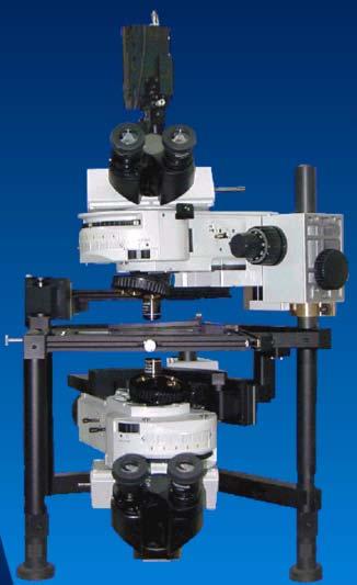
15 NSOM Today: Similar to Standard Scanning Probe Microscopy with an Optical Channel Mechanical Translation stage, piezoelectric scanner Feedback Control (Z distance) Anti-vibration optical table Electrical Scanning drivers for piezoelectric scanner z distance control Amplifiers, Signal processors Software and Computer Optical Light source (lasers), Fiber, Mirrors, Lenses, Objectives Photon detectors (Photon Multiplier Tube, Avalanche Photo Diode, Charge Coupled Devices) Probe to provide the window to the near-field November 2, 6 15
.")
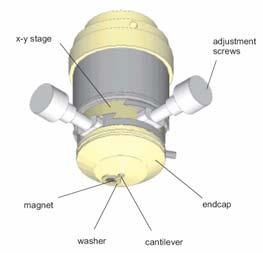
16 Z Distance Control Shear force Normal force Science, 257, (1992). Veeco Instruments Nanonics Imaging Ltd Witec GmbH November 2, 6 16
 Other kinds, such as tetrahedral tip, Fluorescent tip Metal")

17 NSOM Probes Aperture type Taped fiber, multiple-taped fiber Cantilevered AFM/NSOM tips (Si 3 N 4, SiO 2 ) Other kinds, such as tetrahedral tip, Fluorescent tip Metal Coating Optional Apertureless type Dielectrics, semiconductors or metals Other kinds, such as nano-particle attached tip Nanonics Imaging Ltd Witec GmbH November 2, 6 17


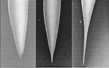
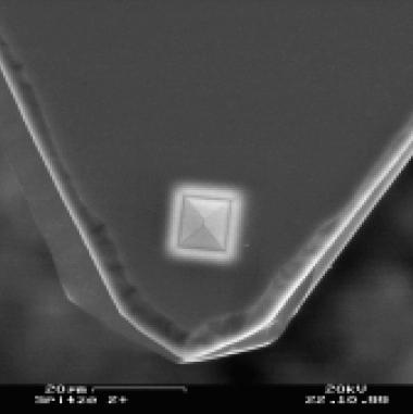
18 Probe Fabrication: Fiber probes Lazarev, A., Rev. Sci. Inst., 74, (3). November 2, 6 18
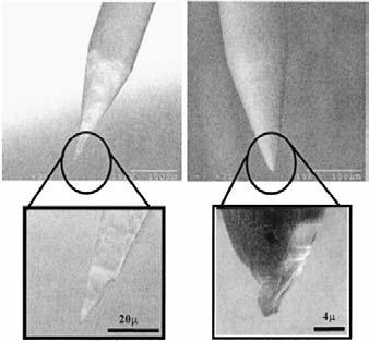
19 Probe Fabrication: Cantilevered probes Mircofabrication Rubbing Focus ion beam milling Special techniques, such as solid electrolysis, self-terminated corrosion November 2, 6 19

.")
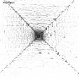
20 Mirco-fabrication: a batch process App. Phy. Lett., 68, (1996). November 2, 6 20

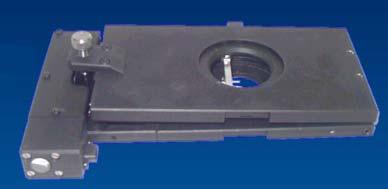
21 Commercial NSOM: Nanonics MultiView 0 APD Probe Laser Scanner Nanonics Imaging Ltd November 2, 6 21


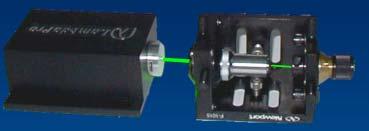
22 Commercial NSOM: Witec ALphaSNOM Cantilevered probe Aperture Probe Mounting Witec GmbH November 2, 6 22


23 Commercial NSOM: Veeco Aurora3 System schematic Fiber mounting Feedback control Veeco Instruments November 2, 6 23
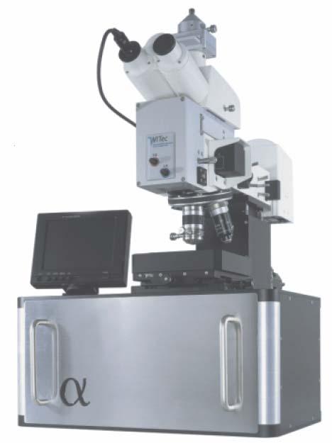
24 Nanonics System at Purdue Nanonics MultiView 0 NSOM / AFM Tuning Fork Feedback Control Normal or Shear Force Aperture tips down to 50 nm AFM tips down to 30 nm Radiation Sources: (532, 633, 785) nm Supercontinuum nm Nanonics Imaging Ltd November 2, 6 24

25 APD Filter Obj. Lens Upper Piezo To Piezoelectrics Fiber Tip HV Source Freq. Gen. 532nm Source Lower Piezo Obj. Lens Tuning Fork Lock-In Detector PID Controller Filter Computer APD Prof. Shalaev s group Internal to Purdue November 2, 6 25

, Proscan software User Interface Prof.")
26 Purdue Homemade NSOM Developed from Commercial AFM Scanning: micro stages, piezoelectic scanner and probe head Imaging: optics with video monitor, white source and HeNe laser System Setup Light detection: Photomultiplier tube (PMT), photon counter Signal Processing: AutoProbe Electronic Module (AEM), Proscan software User Interface Prof. Xianfan Xu s group Internal to Purdue November 2, 6 26
27 Schematic of Purdue Home-made NSOM Video Monitor CCD Computer BS PMT Photon Counter AEM White Source BS PSD AFM/NSOM Probe 20 Objective Diode Probe Head Sample Laser HeNe Laser Scanner Prism Z scanner X,Y scanner Prof. Xianfan Xu s group Internal to Purdue November 2, 6 27
28 Presentation Overview Motivation for nearfield optics Introduction to NSOM What is NSOM today? What can you do with NSOM? November 2, 6 28
29 What Can you do with NSOM? Ultrahigh resolution OPTICAL Imaging / Plamonic studies Spectroscopy Nearfield Surface Enhanced Raman Spectroscopy Local Spectroscopy of Semiconductor Devices Near-field Broadband Spectroscopy Modification of Surfaces Subwavelength photolithography Ultra High Density data storage Laser Ablation Nearfield femtosecond studies November 2, 6 29


30 High Resolution Optical Imaging SEM 83 nm Optical resolution seen with 100 nm tip AFM Obj. Lens NSOM Prof. Shalaev s group Internal to Purdue APD November 2, 6 30
31 NF Surface Enhanced Raman Spectroscopy (SERS) What is Raman spectroscopy? Incident light scattered by a molecule will scatter at different wavelengths than the incident light. Measuring the spectrum of such scattered light provides powerful a fingerprinting technique for identification. What is surface enhanced Raman spectroscopy (SERS)? Typical Raman signals are rather weak. The electromagnetic fields carrying the fingerprinting information can be enhanced by many orders of magnitude. Add in NSOM: The addition of nearfield optics to such techniques enables localization of illumination or collection of light. This provides the means to detect trace amounts that would otherwise be undetectable. November 2, 6 31


32 Nearfield SERS of R6-G on a semi continuous metal film Spectrometer Spectra Spacing: 470 nm AFM 250 #6 400 #8 C / 20 min Reflection NSOM Prof. Shalaev s group Internal to Purdue C / 20 min # # / cm 1 / cm November 2, 6 32
 November 2,")
33 NF Spectroscopy: Quantum Device Science 264, 1740 (1994) November 2, 6 33
34 NF Spectroscopy: Broadband Tuning Fork (for feedback control) Photonic Crystal Fibre with broadband output Tapered Fibre Probe Sample Scanning xyz piezo stage YAG 1064 nm Objective Lens 100x 0.75NA Spectrometer Si CCD Prof. Shalaev s group Internal to Purdue November 2, 6 34
 Optics Letters, Vol.30, No.")
 = I(x,y,λ)/I o (λ) Counts 0 1500 1000 500 633 SMF probe with red")

35 NF Broadband Spectroscopy Local Transmittance Representative AFM Laser Phys. Lett. 3, No. 1, (6) Optics Letters, Vol.30, No.24, 3356 (5) 2500 Reference Spectrum nm integrated Transmittance Mapping Function: T (x,y,λ) = I(x,y,λ)/I o (λ) Counts SMF probe with red Filter WaveLength(nm) nm nm November 2, 6 35 Prof. Shalaev s group Internal to Purdue
36 g g g g g g g g g g g g NF Broadband imaging g g g g g g g g g g g g Mode Transition as function of Wavelength 1500 nm g g g g g g g g g g g g nm November 2, 6 36 Prof. Shalaev s group Internal to Purdue
37 Subwavelength Photolithography Use NSOM to write patterns into a photoresist Can use aperture NSOM in illumination mode Can use apertureless NSOM utilizing two photon absorption at the metallic tip November 2, 6 37

38 Ultrahigh Density Data Storage Can use aperture NSOM in illumination mode to both write and read data on magneto-optical material When writing, probe heats the medium under the probe. The domain under the write beam becomes magnetized opposite of the surrounding material. This varying domain of magnetization can then be read using the same probe, but with a lower output power. Appl. Phys. Lett. 61, (1992) November 2, 6 38

 J.")
39 Nearfield femtosecond studies Pump Probe techniques NSOM allows this technique to employ spatial localization to measure carrier dynamics. (eg in semiconductor devices) Localized laser ablation Currently in use for photomask repair Nanolithography Rev. Sci. Inst. 70, 2758 (1999) J. Microscopy 194, 537 (1999) November 2, 6 39
40 Other things done with NSOM Fluorescent spectrum studies of biological cells, molecules and DNA Atom trapping and Manipulation Local probing of luminescent devices Low temperature NSOM Surface plasmon / Local field enhancement November 2, 6 40
41 Recap Nearfield Scanning Optical Microscopy (NSOM) NSOM is a relatively new technology that defeats the diffraction limit for optical measurements. Utilizes the near field portion of electromagnetism to window down to ~ 10 nm spatial resolution. NSOM instrumentation has progressively developed over the past 15 years, to the point where several different basic techniques are available as commercial instruments The principles of NSOM are very much in play within the research community. It has many different applications ranging from biological studies to nanofabrication. Up to Date Near-Field Optics Research NSOM Conference: NFO9 September 6, look for conference proceedings in the Journal of Microscopy, 7 Quick and Easy Resources Review Articles: R.C. Dunn. Chemical Reviews, 99 (1999) B. Hecht, B. Sick, U.P. Wild, V. Deckert, R. Zenobi, O.J.F. Martin, and D.W. Pohl. Journal of Chemical Physics, 112 (0) Website: Olympus Microscopy (nearfield section) November 2, 6 41
NSOM (SNOM) Overview
 Overview") NSOM (SNOM) Overview The limits of far field imaging In the early 1870s, Ernst Abbe formulated a rigorous criterion for being able to resolve two objects in a light microscope: d > ë / (2sinè) where d
NSOM (SNOM) Overview The limits of far field imaging In the early 1870s, Ernst Abbe formulated a rigorous criterion for being able to resolve two objects in a light microscope: d > ë / (2sinè) where d
PH880 Topics in Physics
 PH880 Topics in Physics Modern Optical Imaging (Fall 2010) Overview of week 12 Monday: FRET Wednesday: NSOM Förster resonance energy transfer (FRET) Fluorescence emission i FRET Donor Acceptor wikipedia
Microscopic Structures
 Microscopic Structures Image Analysis Metal, 3D Image (Red-Green) The microscopic methods range from dark field / bright field microscopy through polarisation- and inverse microscopy to techniques like
Nanonics Systems are the Only SPMs that Allow for On-line Integration with Standard MicroRaman Geometries
 Nanonics Systems are the Only SPMs that Allow for On-line Integration with Standard MicroRaman Geometries 2002 Photonics Circle of Excellence Award PLC Ltd, England, a premier provider of Raman microspectral
attosnom I: Topography and Force Images NANOSCOPY APPLICATION NOTE M06 RELATED PRODUCTS G
 APPLICATION NOTE M06 attosnom I: Topography and Force Images Scanning near-field optical microscopy is the outstanding technique to simultaneously measure the topography and the optical contrast of a sample.
- Near Field Scanning Optical Microscopy - Electrostatic Force Microscopy - Magnetic Force Microscopy
 - Near Field Scanning Optical Microscopy - Electrostatic Force Microscopy - Magnetic Force Microscopy Yongho Seo Near-field Photonics Group Leader Wonho Jhe Director School of Physics and Center for Near-field
Administrative details:
 Administrative details: Anything from your side? www.photonics.ethz.ch 1 What are we actually doing here? Optical imaging: Focusing by a lens Angular spectrum Paraxial approximation Gaussian beams Method
Study of shear force as a distance regulation mechanism for scanning near-field optical microscopy
 Study of shear force as a distance regulation mechanism for scanning near-field optical microscopy C. Durkan a) and I. V. Shvets Department of Physics, Trinity College Dublin, Ireland Received 31 May 1995;
Nanolithography using high transmission nanoscale ridge aperture probe
 Purdue University Purdue e-pubs Birck and NCN Publications Birck Nanotechnology Center 12-2008 Nanolithography using high transmission nanoscale ridge aperture probe Nicholas Murphy-DuBay Purdue University
3D simulations of the experimental signal measured in near-field optical microscopy
 Journal of Microscopy, Vol. 194, Pt 2/3, May/June 1999, pp. 235 239. Received 6 December 1998; accepted 4 February 1999 3D simulations of the experimental signal measured in near-field optical microscopy
International Journal of Nano Dimension
 ISSN: 2008-8868 Contents list available at IJND International Journal of Nano Dimension Journal homepage: www.ijnd.ir Review article An overview of scanning near-field optical microscopy in characterization
Nanoscale Systems for Opto-Electronics
 Nanoscale Systems for Opto-Electronics 675 PL intensity [arb. units] 700 Wavelength [nm] 650 625 600 5µm 1.80 1.85 1.90 1.95 Energy [ev] 2.00 2.05 1 Nanoscale Systems for Opto-Electronics Lecture 5 Interaction
RECENTLY, using near-field scanning optical
 1 2 1 2 Theoretical and Experimental Study of Near-Field Beam Properties of High Power Laser Diodes W. D. Herzog, G. Ulu, B. B. Goldberg, and G. H. Vander Rhodes, M. S. Ünlü L. Brovelli, C. Harder Abstract
Enhanced transmission in near-field imaging of layered plasmonic structures
 Enhanced transmission in near-field imaging of layered plasmonic structures Reuben M. Bakker, Vladimir P. Drachev, Hsiao-Kuan Yuan and Vladimir M. Shalaev School of Electrical and Computer Engineering,
with valuable information only accessible with optical contrast. One should look at it as a complementary tool with some room for improvement.
 Introduction Optical microscopy has come a long way from Zacharias Jansen s first microscope at the end of the 16th century to today s highly developed microscopes. A number of different contrast mechanisms
Spectral phase shaping for high resolution CARS spectroscopy around 3000 cm 1
 Spectral phase shaping for high resolution CARS spectroscopy around 3 cm A.C.W. van Rhijn, S. Postma, J.P. Korterik, J.L. Herek, and H.L. Offerhaus Mesa + Research Institute for Nanotechnology, University
Investigation of the Near-field Distribution at Novel Nanometric Aperture Laser
 Investigation of the Near-field Distribution at Novel Nanometric Aperture Laser Tiejun Xu, Jia Wang, Liqun Sun, Jiying Xu, Qian Tian Presented at the th International Conference on Electronic Materials
Near-field optical photomask repair with a femtosecond laser
 Journal of Microscopy, Vol. 194, Pt 2/3, May/June 1999, pp. 537 541. Received 6 December 1998; accepted 9 February 1999 Near-field optical photomask repair with a femtosecond laser K. LIEBERMAN, Y. SHANI,
Lecture 20: Optical Tools for MEMS Imaging
 MECH 466 Microelectromechanical Systems University of Victoria Dept. of Mechanical Engineering Lecture 20: Optical Tools for MEMS Imaging 1 Overview Optical Microscopes Video Microscopes Scanning Electron
Near-field Optical Microscopy
 Near-field Optical Microscopy R. Fernandez, X. Wang, N. Li, K. Parker, and A. La Rosa Physics Department Portland State University Portland, Oregon Near-Field SPIE Optics Microscopy East 2005 Group PSU
Heisenberg) relation applied to space and transverse wavevector
 relation applied to space and transverse wavevector") 2. Optical Microscopy 2.1 Principles A microscope is in principle nothing else than a simple lens system for magnifying small objects. The first lens, called the objective, has a short focal length (a
2. Optical Microscopy 2.1 Principles A microscope is in principle nothing else than a simple lens system for magnifying small objects. The first lens, called the objective, has a short focal length (a
Fabrication of Probes for High Resolution Optical Microscopy
 Fabrication of Probes for High Resolution Optical Microscopy Physics 564 Applied Optics Professor Andrès La Rosa David Logan May 27, 2010 Abstract Near Field Scanning Optical Microscopy (NSOM) is a technique
Resolution. Diffraction from apertures limits resolution. Rayleigh criterion θ Rayleigh = 1.22 λ/d 1 peak at 2 nd minimum. θ f D
 Microscopy Outline 1. Resolution and Simple Optical Microscope 2. Contrast enhancement: Dark field, Fluorescence (Chelsea & Peter), Phase Contrast, DIC 3. Newer Methods: Scanning Tunneling microscopy (STM),
BASICS OF CONFOCAL IMAGING (PART I)
") BASICS OF CONFOCAL IMAGING (PART I) INTERNAL COURSE 2012 LIGHT MICROSCOPY Lateral resolution Transmission Fluorescence d min 1.22 NA obj NA cond 0 0 rairy 0.61 NAobj Ernst Abbe Lord Rayleigh Depth of field
BASICS OF CONFOCAL IMAGING (PART I) INTERNAL COURSE 2012 LIGHT MICROSCOPY Lateral resolution Transmission Fluorescence d min 1.22 NA obj NA cond 0 0 rairy 0.61 NAobj Ernst Abbe Lord Rayleigh Depth of field
Beams and Scanning Probe Microscopy
 IFN-CNR, Sezione di Trento Istituto Trentino di Cultura of Trento Department of Physics University of Trento Towards the joint use of X-ray Beams and Scanning Probe Microscopy Silvia Larcheri SILS 2005
Analytical analysis of modulated signal in apertureless scanning near-field optical microscopy C. H. Chuang and Y. L. Lo *
 Research Express@NCKU Volume 5 Issue 10 - October 3, 2008 [ http://research.ncku.edu.tw/re/articles/e/20081003/2.html ] Analytical analysis of modulated signal in apertureless scanning near-field optical
Chemical Imaging. Whiskbroom Imaging. Staring Imaging. Pushbroom Imaging. Whiskbroom. Staring. Pushbroom
 Chemical Imaging Whiskbroom Chemical Imaging (CI) combines different technologies like optical microscopy, digital imaging and molecular spectroscopy in combination with multivariate data analysis methods.
Devices Imaged with Near-eld Scanning Optical Microscopy. G. H. Vander Rhodes, M. S. Unlu, and B. B. Goldberg. J. M. Pomeroy
 Internal Spatial Modes of One Dimensional Photonic Band Gap Devices Imaged with Near-eld Scanning Optical Microscopy G. H. Vander Rhodes, M. S. Unlu, and B. B. Goldberg Departments of Physics and Electrical
Three-dimensional imaging with optical tweezers
 Three-dimensional imaging with optical tweezers M. E. J. Friese, A. G. Truscott, H. Rubinsztein-Dunlop, and N. R. Heckenberg We demonstrate a three-dimensional scanning probe microscope in which the extremely
:... resolution is about 1.4 μm, assumed an excitation wavelength of 633 nm and a numerical aperture of 0.65 at 633 nm.
 PAGE 30 & 2008 2007 PRODUCT CATALOG Confocal Microscopy - CFM fundamentals :... Over the years, confocal microscopy has become the method of choice for obtaining clear, three-dimensional optical images
plasmonic nanoblock pair
 Nanostructured potential of optical trapping using a plasmonic nanoblock pair Yoshito Tanaka, Shogo Kaneda and Keiji Sasaki* Research Institute for Electronic Science, Hokkaido University, Sapporo 1-2,
Supplementary Materials for
 advances.sciencemag.org/cgi/content/full/4/2/e1700324/dc1 Supplementary Materials for Photocarrier generation from interlayer charge-transfer transitions in WS2-graphene heterostructures Long Yuan, Ting-Fung
Dielectric Contrast Imaging Using Apertureless Scanning Near-Field Optical Microscopy in the Reflection Mode
 Journal of the Korean Physical Society, Vol. 47, August 2005, pp. S140 S146 Dielectric Contrast Imaging Using Apertureless Scanning Near-Field Optical Microscopy in the Reflection Mode Debdulal Roy, S.
Effective Image and Spectral Data Acquisition Method Used in Scanning Near-field Optical Microscopy by Bimorph-based Shear Force Sensor
 Effective Image and Spectral Data Acquisition Method Used in Scanning Near-field Optical Microscopy by Bimorph-based Shear Force Sensor Wei Cai, Mu Yang, Yingjie Wang, and Guangyi Shang* Department of
Applications of Steady-state Multichannel Spectroscopy in the Visible and NIR Spectral Region
 Feature Article JY Division I nformation Optical Spectroscopy Applications of Steady-state Multichannel Spectroscopy in the Visible and NIR Spectral Region Raymond Pini, Salvatore Atzeni Abstract Multichannel
Nanopatterning using NSOM probes integrated with high transmission nanoscale bowtie aperture
 Nanopatterning using NSOM probes integrated with high transmission nanoscale bowtie aperture Nicholas Murphy-DuBay, Liang Wang, Edward C. Kinzel, Sreemanth M. V. Uppuluri, and X. Xu * School of Mechanical
Lecture 21. Wind Lidar (3) Direct Detection Doppler Lidar
 Direct Detection Doppler Lidar") Lecture 21. Wind Lidar (3) Direct Detection Doppler Lidar Overview of Direct Detection Doppler Lidar (DDL) Resonance fluorescence DDL Fringe imaging DDL Scanning FPI DDL FPI edge-filter DDL Absorption
Lecture 21. Wind Lidar (3) Direct Detection Doppler Lidar Overview of Direct Detection Doppler Lidar (DDL) Resonance fluorescence DDL Fringe imaging DDL Scanning FPI DDL FPI edge-filter DDL Absorption
MEMS for RF, Micro Optics and Scanning Probe Nanotechnology Applications
 MEMS for RF, Micro Optics and Scanning Probe Nanotechnology Applications Part I: RF Applications Introductions and Motivations What are RF MEMS? Example Devices RFIC RFIC consists of Active components
Basics of confocal imaging (part I)
") Basics of confocal imaging (part I) Swiss Institute of Technology (EPFL) Faculty of Life Sciences Head of BIOIMAGING AND OPTICS BIOP arne.seitz@epfl.ch Lateral resolution BioImaging &Optics Platform Light
Basics of confocal imaging (part I) Swiss Institute of Technology (EPFL) Faculty of Life Sciences Head of BIOIMAGING AND OPTICS BIOP arne.seitz@epfl.ch Lateral resolution BioImaging &Optics Platform Light
Femtosecond laser microfabrication in. Prof. Dr. Cleber R. Mendonca
 Femtosecond laser microfabrication in polymers Prof. Dr. Cleber R. Mendonca laser microfabrication focus laser beam on material s surface laser microfabrication laser microfabrication laser microfabrication
attocfm I for Surface Quality Inspection NANOSCOPY APPLICATION NOTE M01 RELATED PRODUCTS G
 APPLICATION NOTE M01 attocfm I for Surface Quality Inspection Confocal microscopes work by scanning a tiny light spot on a sample and by measuring the scattered light in the illuminated volume. First,
Near Field Optical Microscopy Characterization of IC Metrology
 Rochester Institute of Technology RIT Scholar Works Presentations and other scholarship 5-1-1994 Near Field Optical Microscopy Characterization of IC Metrology Ricardo Toledo-Crow Rochester Institute of
NanoFocus Inc. Next Generation Scanning Probe Technology. Tel : Fax:
 NanoFocus Inc. Next Generation Scanning Probe Technology www.nanofocus.kr Tel : 82-2-864-3955 Fax: 82-2-864-3956 Albatross SPM is Multi functional research grade system Flexure scanner and closed-loop
Near Field Scanning Optical Microscopy(NSOM) of nano devices
 of nano devices") Calhoun: The NPS Institutional Archive Theses and Dissertations Thesis Collection 2008-12 Near Field Scanning Optical Microscopy(NSOM) of nano devices Low, Chun Hong Monterey California. Naval Postgraduate
Calhoun: The NPS Institutional Archive Theses and Dissertations Thesis Collection 2008-12 Near Field Scanning Optical Microscopy(NSOM) of nano devices Low, Chun Hong Monterey California. Naval Postgraduate
Near-field optics: from subwavelength illumination to nanometric shadowing
 FOCUS ON OPTICAL IMAGING Near-field optics: from subwavelength illumination to nanometric shadowing Aaron Lewis, Hesham Taha, Alina Strinkovski, Alexandra Manevitch, Artium Khatchatouriants, Rima Dekhter
We are IntechOpen, the world s leading publisher of Open Access books Built by scientists, for scientists. International authors and editors
 We are IntechOpen, the world s leading publisher of Open Access books Built by scientists, for scientists 3,500 108,000 1.7 M Open access books available International authors and editors Downloads Our
k λ NA Resolution of optical systems depends on the wavelength visible light λ = 500 nm Extreme ultra-violet and soft x-ray light λ = 1-50 nm
 Resolution of optical systems depends on the wavelength visible light λ = 500 nm Spatial Resolution = k λ NA EUV and SXR microscopy can potentially resolve full-field images with 10-100x smaller features
Redefining Measurement ID101 OEM Visible Photon Counter
 Redefining Measurement ID OEM Visible Photon Counter Miniature Photon Counter for OEM Applications Intended for large-volume OEM applications, the ID is the smallest, most reliable and most efficient single-photon
Lecture 27. Wind Lidar (6) Edge Filter-Based Direct Detection Doppler Lidar
 Edge Filter-Based Direct Detection Doppler Lidar") Lecture 27. Wind Lidar (6) Edge Filter-Based Direct Detection Doppler Lidar q FPI and Fizeau edge-filter DDL q Iodine-absorption-line edge-filter DDL q Edge-filter lidar data retrieval and error analysis
Lecture 27. Wind Lidar (6) Edge Filter-Based Direct Detection Doppler Lidar q FPI and Fizeau edge-filter DDL q Iodine-absorption-line edge-filter DDL q Edge-filter lidar data retrieval and error analysis
Applications of Optics
 Nicholas J. Giordano www.cengage.com/physics/giordano Chapter 26 Applications of Optics Marilyn Akins, PhD Broome Community College Applications of Optics Many devices are based on the principles of optics
photolithographic techniques (1). Molybdenum electrodes (50 nm thick) are deposited by
. Molybdenum electrodes (50 nm thick) are deposited by") Supporting online material Materials and Methods Single-walled carbon nanotube (SWNT) devices are fabricated using standard photolithographic techniques (1). Molybdenum electrodes (50 nm thick) are deposited
Supporting online material Materials and Methods Single-walled carbon nanotube (SWNT) devices are fabricated using standard photolithographic techniques (1). Molybdenum electrodes (50 nm thick) are deposited
Microscopy Techniques that make it easy to see things this small.
 Microscopy Techniques that make it easy to see things this small. What is a Microscope? An instrument for viewing objects that are too small to be seen easily by the naked eye. Dutch spectacle-makers Hans
A Narrow-Band Tunable Diode Laser System with Grating Feedback
 A Narrow-Band Tunable Diode Laser System with Grating Feedback S.P. Spirydovich Draft Abstract The description of diode laser was presented. The tuning laser system was built and aligned. The free run
Εισαγωγική στην Οπτική Απεικόνιση
 Εισαγωγική στην Οπτική Απεικόνιση Δημήτριος Τζεράνης, Ph.D. Εμβιομηχανική και Βιοϊατρική Τεχνολογία Τμήμα Μηχανολόγων Μηχανικών Ε.Μ.Π. Χειμερινό Εξάμηνο 2015 Light: A type of EM Radiation EM radiation:
Combined SNOM/AFM microscopy with micromachined nanoapertures
 Materials Science, Vol. 21, No. 3, 2003 Combined SNOM/AFM microscopy with micromachined nanoapertures JACEK RADOJEWSKI 1*, PIOTR GRABIEC 2 1 Faculty of Microsystem Electronics and Photonics, Wrocław University
Spectrometer using a tunable diode laser
 Spectrometer using a tunable diode laser Ricardo Vasquez Department of Physics, Purdue University, West Lafayette, IN April, 2000 In the following paper the construction of a simple spectrometer using
Measurement of Microscopic Three-dimensional Profiles with High Accuracy and Simple Operation
 238 Hitachi Review Vol. 65 (2016), No. 7 Featured Articles Measurement of Microscopic Three-dimensional Profiles with High Accuracy and Simple Operation AFM5500M Scanning Probe Microscope Satoshi Hasumura
Advanced Nanoscale Metrology with AFM
 Advanced Nanoscale Metrology with AFM Sang-il Park Corp. SPM: the Key to the Nano World Initiated by the invention of STM in 1982. By G. Binnig, H. Rohrer, Ch. Gerber at IBM Zürich. Expanded by the invention
Moving from micro- to nanoworld in optical domain scanning probe microscopy
 BULLETIN OF THE POLISH ACADEMY OF SCIENCES TECHNICAL SCIENCES Vol. 54, No. 1, 2006 Moving from micro- to nanoworld in optical domain scanning probe microscopy J. RADOJEWSKI Faculty of Microsystem Electronics
SPECIAL TOPIC: NEAR-FIELD MICROSCOPY AND SPECTROSCOPY. Scanning near-field optical microscopy with aperture probes: Fundamentals and applications
 JOURNAL OF CHEMICAL PHYSICS VOLUME 112, NUMBER 18 8 MAY 2000 SPECIAL TOPIC: NEAR-FIELD MICROSCOPY AND SPECTROSCOPY Scanning near-field optical microscopy with aperture probes: Fundamentals and applications
SUPPLEMENTARY INFORMATION
 SUPPLEMENTARY INFORMATION DOI: 10.1038/NNANO.2015.137 Controlled steering of Cherenkov surface plasmon wakes with a one-dimensional metamaterial Patrice Genevet *, Daniel Wintz *, Antonio Ambrosio *, Alan
A novel tunable diode laser using volume holographic gratings
 A novel tunable diode laser using volume holographic gratings Christophe Moser *, Lawrence Ho and Frank Havermeyer Ondax, Inc. 85 E. Duarte Road, Monrovia, CA 9116, USA ABSTRACT We have developed a self-aligned
SUPPLEMENTARY INFORMATION
 SUPPLEMENTARY INFORMATION Supplementary Information Real-space imaging of transient carrier dynamics by nanoscale pump-probe microscopy Yasuhiko Terada, Shoji Yoshida, Osamu Takeuchi, and Hidemi Shigekawa*
Waveguide-based single-pixel up-conversion infrared spectrometer
 Waveguide-based single-pixel up-conversion infrared spectrometer Qiang Zhang 1,2, Carsten Langrock 1, M. M. Fejer 1, Yoshihisa Yamamoto 1,2 1. Edward L. Ginzton Laboratory, Stanford University, Stanford,
Cavity QED with quantum dots in semiconductor microcavities
 Cavity QED with quantum dots in semiconductor microcavities M. T. Rakher*, S. Strauf, Y. Choi, N.G. Stolz, K.J. Hennessey, H. Kim, A. Badolato, L.A. Coldren, E.L. Hu, P.M. Petroff, D. Bouwmeester University
Mode analysis of Oxide-Confined VCSELs using near-far field approaches
 Annual report 998, Dept. of Optoelectronics, University of Ulm Mode analysis of Oxide-Confined VCSELs using near-far field approaches Safwat William Zaki Mahmoud We analyze the transverse mode structure
Akinori Mitani and Geoff Weiner BGGN 266 Spring 2013 Non-linear optics final report. Introduction and Background
 Akinori Mitani and Geoff Weiner BGGN 266 Spring 2013 Non-linear optics final report Introduction and Background Two-photon microscopy is a type of fluorescence microscopy using two-photon excitation. It
Direct observation of beamed Raman scattering
 Supporting Information Direct observation of beamed Raman scattering Wenqi Zhu, Dongxing Wang, and Kenneth B. Crozier* School of Engineering and Applied Sciences, Harvard University, Cambridge, Massachusetts
Waveguiding in PMMA photonic crystals
 ROMANIAN JOURNAL OF INFORMATION SCIENCE AND TECHNOLOGY Volume 12, Number 3, 2009, 308 316 Waveguiding in PMMA photonic crystals Daniela DRAGOMAN 1, Adrian DINESCU 2, Raluca MÜLLER2, Cristian KUSKO 2, Alex.
NanoSpective, Inc Progress Drive Suite 137 Orlando, Florida
 TEM Techniques Summary The TEM is an analytical instrument in which a thin membrane (typically < 100nm) is placed in the path of an energetic and highly coherent beam of electrons. Typical operating voltages
Comparison of resolution specifications for micro- and nanometer measurement techniques
 P4.5 Comparison of resolution specifications for micro- and nanometer measurement techniques Weckenmann/Albert, Tan/Özgür, Shaw/Laura, Zschiegner/Nils Chair Quality Management and Manufacturing Metrology
Contact optical nanolithography using nanoscale C-shaped apertures
 Contact optical nanolithography using nanoscale C-shaped s Liang Wang, Eric X. Jin, Sreemanth M. Uppuluri, and Xianfan Xu School of Mechanical Engineering, Purdue University, West Lafayette, Indiana 47907
Optical Microscope. Active anti-vibration table. Mechanical Head. Computer and Software. Acoustic/Electrical Shield Enclosure
 Optical Microscope On-axis optical view with max. X magnification Motorized zoom and focus Max Field of view: mm x mm (depends on zoom) Resolution : um Working Distance : mm Magnification : max. X Zoom
SUPPLEMENTARY INFORMATION
 Optically reconfigurable metasurfaces and photonic devices based on phase change materials S1: Schematic diagram of the experimental setup. A Ti-Sapphire femtosecond laser (Coherent Chameleon Vision S)
S200 Course LECTURE 1 TEM
 S200 Course LECTURE 1 TEM Development of Electron Microscopy 1897 Discovery of the electron (J.J. Thompson) 1924 Particle and wave theory (L. de Broglie) 1926 Electromagnetic Lens (H. Busch) 1932 Construction
Confocal Imaging Through Scattering Media with a Volume Holographic Filter
 Confocal Imaging Through Scattering Media with a Volume Holographic Filter Michal Balberg +, George Barbastathis*, Sergio Fantini % and David J. Brady University of Illinois at Urbana-Champaign, Urbana,
; A=4π(2m) 1/2 /h. exp (Fowler Nordheim Eq.) 2 const
 1/2 /h. exp (Fowler Nordheim Eq.) 2 const") Scanning Tunneling Microscopy (STM) Brief background: In 1981, G. Binnig, H. Rohrer, Ch. Gerber and J. Weibel observed vacuum tunneling of electrons between a sharp tip and a platinum surface. The tunnel
Scanning Tunneling Microscopy (STM) Brief background: In 1981, G. Binnig, H. Rohrer, Ch. Gerber and J. Weibel observed vacuum tunneling of electrons between a sharp tip and a platinum surface. The tunnel
OPTICAL SENSORS-CONSTRUCTION ALTERNATIVES
 OPTICAL SENSORS-CONSTRUCTION ALTERNATIVES Mariana ENACHE, Cristina ŢUINEA BOBE Universitatea Valahia Târgovişte, Facultatea Ştiinta si Ingineria Materialelor, B-dul Regele Carol I, Nr.2, 0200, Târgovişte,
Impact of the light coupling on the sensing properties of photonic crystal cavity modes Kumar Saurav* a,b, Nicolas Le Thomas a,b,
 Impact of the light coupling on the sensing properties of photonic crystal cavity modes Kumar Saurav* a,b, Nicolas Le Thomas a,b, a Photonics Research Group, Ghent University-imec, Technologiepark-Zwijnaarde
Photonic Crystal Slot Waveguide Spectrometer for Detection of Methane
 Photonic Crystal Slot Waveguide Spectrometer for Detection of Methane Swapnajit Chakravarty 1, Wei-Cheng Lai 2, Xiaolong (Alan) Wang 1, Che-Yun Lin 2, Ray T. Chen 1,2 1 Omega Optics, 10306 Sausalito Drive,
Ultrafast Beams and Applications UBA July, 2017 Presenter: Arsham Yeremyan
 Laser driven facility for irradiation experiments, two-photon microscopy and microfabrication Ultrafast Beams and Applications UBA17 04-07 July, 2017 Presenter: Arsham Yeremyan Outline Parallel operation
Low-energy Electron Diffractive Imaging for Three dimensional Light-element Materials
 Low-energy Electron Diffractive Imaging for Three dimensional Light-element Materials Hitachi Review Vol. 61 (2012), No. 6 269 Osamu Kamimura, Ph. D. Takashi Dobashi OVERVIEW: Hitachi has been developing
CONFIGURING. Your Spectroscopy System For PEAK PERFORMANCE. A guide to selecting the best Spectrometers, Sources, and Detectors for your application
 CONFIGURING Your Spectroscopy System For PEAK PERFORMANCE A guide to selecting the best Spectrometers, s, and s for your application Spectral Measurement System Spectral Measurement System Spectrograph
picoemerald Tunable Two-Color ps Light Source Microscopy & Spectroscopy CARS SRS
 picoemerald Tunable Two-Color ps Light Source Microscopy & Spectroscopy CARS SRS 1 picoemerald Two Colors in One Box Microscopy and Spectroscopy with a Tunable Two-Color Source CARS and SRS microscopy
You won t be able to measure the incident power precisely. The readout of the power would be lower than the real incident power.
 1. a) Given the transfer function of a detector (below), label and describe these terms: i. dynamic range ii. linear dynamic range iii. sensitivity iv. responsivity b) Imagine you are using an optical
Probe NanoLaboratory. NTEGRA Spectra. Upright configuration. Instruction Manual
 NTEGRA Probe NanoLaboratory NTEGRA Spectra Upright configuration Instruction Manual ` NTEGRA Spectra Probe NanoLaboratory (Upright Configuration with Solar TII Spectrometer) Instruction Manual 1 February
An apertureless near-field scanning optical microscope for imaging surface plasmons in the mid-wave infrared
 An apertureless near-field scanning optical microscope for imaging surface plasmons in the mid-wave infrared John Kohoutek, Dibyendu Dey, Ryan Gelfand, Alireza Bonakdar, Hooman Mohseni Bio-Inspired Sensors
Observing Microorganisms through a Microscope LIGHT MICROSCOPY: This type of microscope uses visible light to observe specimens. Compound Light Micros
 PHARMACEUTICAL MICROBIOLOGY JIGAR SHAH INSTITUTE OF PHARMACY NIRMA UNIVERSITY Observing Microorganisms through a Microscope LIGHT MICROSCOPY: This type of microscope uses visible light to observe specimens.
Scanning Tunneling Microscopy
 EMSE-515 02 Scanning Tunneling Microscopy EMSE-515 F. Ernst 1 Scanning Tunneling Microscope: Working Principle 2 Scanning Tunneling Microscope: Construction Principle 1 sample 2 sample holder 3 clamps
COMPONENTS OF OPTICAL INSTRUMENTS. Chapter 7 UV, Visible and IR Instruments
 COMPONENTS OF OPTICAL INSTRUMENTS Chapter 7 UV, Visible and IR Instruments 1 Topics A. GENERAL DESIGNS B. SOURCES C. WAVELENGTH SELECTORS D. SAMPLE CONTAINERS E. RADIATION TRANSDUCERS F. SIGNAL PROCESSORS
COMPONENTS OF OPTICAL INSTRUMENTS. Topics
 COMPONENTS OF OPTICAL INSTRUMENTS Chapter 7 UV, Visible and IR Instruments Topics A. GENERAL DESIGNS B. SOURCES C. WAVELENGTH SELECTORS D. SAMPLE CONTAINERS E. RADIATION TRANSDUCERS F. SIGNAL PROCESSORS
FRAUNHOFER INSTITUTE FOR PHOTONIC MICROSYSTEMS IPMS. Application Area. Quality of Life
 FRAUNHOFER INSTITUTE FOR PHOTONIC MICROSYSTEMS IPMS Application Area Quality of Life Overlay image of visible spectral range (VIS) and thermal infrared range (LWIR). Quality of Life With extensive experience
Index. band bending 317 bandwidth limitation 176, 182, 190, 195, 196 BBO
 Index β-bab 2O 4 (BBO) 85, 202 β-barium borate see β-bab 2O 4 (BBO) β (BEDT-TTF) 2PF 6 299 π-conjugated polymer 304 III-V compound semiconductor 363 III-V-N compound semiconductor 363 4-f chirp compensator
Direct Measurement of Optical Cross-talk in Silicon Photomultipliers Using Light Emission Microscopy
 Direct Measurement of Optical Cross-talk in Silicon Photomultipliers Using Light Emission Microscopy Derek Strom, Razmik Mirzoyan, Jürgen Besenrieder Max-Planck-Institute for Physics, Munich, Germany 14
Lecture 25. Wind Lidar (3) Direct Detection Doppler Lidar
 Direct Detection Doppler Lidar") Lecture 25. Wind Lidar (3) Direct Detection Doppler Lidar Overview of Direct Detection Doppler Lidar (DDL) Fringe imaging DDL Scanning FPI DDL FPI edge-filter DDL Iodine absorption-line edge-filter DDL
Lecture 25. Wind Lidar (3) Direct Detection Doppler Lidar Overview of Direct Detection Doppler Lidar (DDL) Fringe imaging DDL Scanning FPI DDL FPI edge-filter DDL Iodine absorption-line edge-filter DDL
Supporting Information: Plasmonic and Silicon Photonic Waveguides
 Supporting Information: Efficient Coupling between Dielectric-Loaded Plasmonic and Silicon Photonic Waveguides Ryan M. Briggs, *, Jonathan Grandidier, Stanley P. Burgos, Eyal Feigenbaum, and Harry A. Atwater,
Design, Fabrication and Characterization of Very Small Aperture Lasers
 372 Progress In Electromagnetics Research Symposium 2005, Hangzhou, China, August 22-26 Design, Fabrication and Characterization of Very Small Aperture Lasers Jiying Xu, Jia Wang, and Qian Tian Tsinghua
MASSACHUSETTS INSTITUTE OF TECHNOLOGY Department of Electrical Engineering and Computer Science
 Student Name Date MASSACHUSETTS INSTITUTE OF TECHNOLOGY Department of Electrical Engineering and Computer Science 6.161 Modern Optics Project Laboratory Laboratory Exercise No. 6 Fall 2010 Solid-State
Angle-resolved cathodoluminescence spectroscopy
 Angle-resolved cathodoluminescence spectroscopy Toon Coenen, Ernst Jan R. Vesseur, and Albert Polman Center for Nanophotonics, FOM Institute AMOLF Science Park 104, 1098 XG Amsterdam, The Netherlands Abstract
Fast Laser Raman Microscope RAMAN
 Fast Laser Raman Microscope RAMAN - 11 www.nanophoton.jp Fast Raman Imaging A New Generation of Raman Microscope RAMAN-11 developed by Nanophoton was created by combining confocal laser microscope technology