Beams and Scanning Probe Microscopy
|
|
|
- Reynold Jordan Watkins
- 5 years ago
- Views:
Transcription

1 IFN-CNR, Sezione di Trento Istituto Trentino di Cultura of Trento Department of Physics University of Trento Towards the joint use of X-ray Beams and Scanning Probe Microscopy Silvia Larcheri SILS 2005 (Frascati)


2 Nano-scale chemical mapping and surface structural modification by joint use of X-ray X microbeams and tip assisted local detection Specific Targeted Research Project (STRP) Supported by European Commission 6 th Framework Programme


3 Scanning Probe Microscopies (SPM) ZnO thin film on Silicon substrate Red corpuscles 1.0µm Gold island on mica substrate Graphite atoms
4 Scanning Probe Microscopies (SPM)
5 X-ray interaction with matter Sample Incident X-rays Transmitted X-rays hν Visible Light XEOL-PLY e - Total Electron Yield (TEY) hν X-rays Fluorescence (FLY) µx X-ray Absorption Fine Structure (XAFS) These signals are able to be collected by a near field probe! Photon energy h ν

6 Local Probe Microscopy X-Ray Absorption Spectroscopy using Synchrotron Radiation Combined Nano-Scale Spectro-Microscopy
7 X-ray Excited Optical Luminescence Energy - site selection Wavelength [nm] X-rays Visible light Sample PL intensity [a.u.] PLY Absorption [a.u] X-ray energy [ev] Energy [ev]

8 XEOL-XAS XAS setup Grating Mirror C C D Controller X-rays Visible light Sample
9 Scanning Near-Field Optical Microscope (SNOM)
10
 Beamline BM 05 (ESRF Grenoble) September")
11 SNOM prototype (Marseille) XEOL-XAS XAS detection set up (Trento) Beamline BM 05 (ESRF Grenoble) September 2005
 Electronics Z coarse movement of the tip Flange for the vacuum chamber Sample holder and")
12 SNOM prototype D. Pailharey, F. Jandard GPEG-CNRS (Marseille) Electronics Z coarse movement of the tip Flange for the vacuum chamber Sample holder and Z-piezo to engage the tip X and Y tip positioning Tip (fixed on the X-ray beam) Piezo scanner


13 Piezo inertial movements

14 XEOL-XAS XAS setup


15 Fabrication techniques Protection-layer etching Heating & Pulling
16 Etched and Pulled Tips

17 Coating equipment V. Sammelselg,, University of Tartu (Estonia)
18 Characterization 1. Scanning Electron Microscopy (SEM) 2. Transmission/collection properties 3. Topographic image of a well-known surface 4. Goniometric characterization

19 Why ZnO thin films? Interesting material for UV photonics, gas sensors, piezoelectric and waveguide devices,, LED, Easy to prepare using many techniques A lot of different nanostructures Two emission bands (visible and UV) Zhong Lin Wang, Materials Today 7, 26 (2004)
20 Optical Luminescence excited by Cu anode 300 dc magnetron sputtering HT2_30s (from met-zn) 341HT_30s ZnOTN_30s TEC1_30s Intensity (a.u) 100 1/2 thick. 338HT_30s 346HT_30s 3%Ta 347HT_30s Intensity (a.u) TEC2_30s TEC3_30s 7%Cd 480HT2_30s %Cd 480LHT_30s Wavelength (nm) 0 TEC4_30s Wavelength (nm)
21 PLY-XANES studies (Beamline BM 08 ESRF Grenoble ) Intensity (a.u./s) Intensity (a.u.) (a) TEC3 TEC5 TEC1 XEOL spectra at 9700 ev (b) Wavelength (nm) TEC5 TEC3 ZnO powder TEC1 PLY-XANES X-ray energy (ev) TEC samples show significant shifts of the XEOL bands in the visible region. PLY-XANES shows significant differences in the local electron density of states between ZnO powder and our nanostructured samples. Changes between different TEC samples might be due to quantum confinement (QC) or to local distortion mainly related to defects or surface states.
22 Comparison between PLY- and FLY-XANES 2.5 ZnO powder: PLY-XANES Intensity (a.u.) TEC5: PLY-XANES TEC5: FLY-XANES X-ray Energy (ev) Changes between PLY- and FLY-XANES spectra of the same sample should be attributed to the peculiar sensitivity of PLY detection mode to the light emitting centers. The origin of these changes is still under study.
23 Future work SNOM PROTOTYPE Absolute alignment Change from grazing to normal incidence Test using laser source and focused and very intense X-ray beamline OPTICAL FIBER PROBES Improve tip shape Full characterization of the optical fiber probes Apertureless probe SAMPLES Detailed study of XAFS spectra from ZnO thin films Selection of other sample suitable both for topography and spectroscopy


24 Scanning Near Field Optical Microscope Current SNOM is directly inspired by the pioneer idea of Synge The tapered and metalized tip has been introduced by E. Betzig et al. Science, 251, 1468 (1991)
25 Generation of Optical Near-Field What happens by shining the light on S? Optical Near Field M.Ohtsu & K.Kobayashi Nuclei and electrons are displaced from their positions and generate electric dipoles p i The electric lines of force connecting the p i are found not only in S but also on its surface; they tend to take the shortest trajectory: this is why the ONF is very thin and localized
26 Detection of Optical Near-Field Introduction of a secondary sphere The ONF cannot be detected like a conventional propagating light because it is localized Detection method: the ONF is disturbed by a secondary sphere P; the disturbed ONF of S is converted to propagating light (scattered light 2) and collected by a photodetector. The two sphere are coupled to each other in response to the incident light but they are mutually isolated material system Optical Near Field M.Ohtsu & K.Kobayashi
27 Electric Field Distribution behind an aperture convolution of the angular spectrum of the incident field and Fourier transform of the aperture B. Hecht et al., J. Chem. Phys., Vol. 12, No. 18, 2000

28 TEC sample and SNOM tip at BM05 (ESRF)

29 TEC sample and SNOM tip at BM05 (ESRF)

30 Al coated tip SEM - 20 KeV, x500
 working with a<40-50 nm is often impossible")
31 Transmission Coefficient of Aperture Probes Attenuation in the taper region depends on the fabrication method reorganization of modes and strong back-reflection B. Hecht et al., J. Chem. Phys. Vol. 12, No. 18, 2000 Attenuation in the sub-λ aperture calculated rigorously by Bethe transmission scales down as a 4 (a denotes aperture diameter) working with a<40-50 nm is often impossible


32 Focused Ion Beam Milling Before... After nm ADVANTAGES clean-cut, circular aperture desired diamete1r (up to 20 nm) higher throughput (up to one order of magnitude) true near-field optical contrast DRAWBACKS extra time added cost failure rate availability of the instrumentation


33 Etching without polymer coating Tube Etching


34 Focus on the body of the optical fiber Focus on the tip Without light coupling With light coupling


35 X-ray Excited Optical Luminescence (XEOL) setup XEOL XEOL X-rays Sample X-rays
36 First Results before applying for Beamtime at Gilda ( ) Photoluminescence (arb.units) ZnO powder RT, Mo anode ZnO:Al 477 ZnO 341 ZnO Wavelength (nm)
37 XANES-XEOL XEOL spectra All our samples 2.0 Intensity (a.u.) ZnO powder (1.3 mg) TEC1 TEC3 TEC5 341HT 346HT (ZnO+W?) 347HT (ZnO:1% Ta+W?) 480HT2 (ZnO:7% Cd) Energy (ev)

38 Formation of ZnO nanostructures by thermal evaporation PL spectra recorded at room temperature. Spectra a, b, and c were recorded from the low temperature site nanowires, the medium temperature site nanoribbons, and the high temperature site needle-like rods, respectively. SEM images showing the three typical morphologies of the asprepared ZnO products: (a) needle-like rods; (b) nanoribbons; (c) nanowires, and (d) their corresponding growing site temperatures. B. D. Yao, Y. F. Chan, and N. Wang, Appl. Phys. Lett (2002).
39 TEC sample characterization Diffracted intensity (a.u.) TEC5 TEC3 TEC1 ZnO powder X-ray diffraction (100) (002) (101) (102) (110) (103) θ (degree) X-ray diffraction reveals an highly (002) oriented crystalline structure. Intensity (photons/sec) 2500 Laser-excited PL after 5 ns after 90 ns 500 after 530 ns Wavelength (nm) TEC samples exhibit a very intense optical luminescence, both XEOL and PL. Time-resolved PL spectra show a very fast excitonic luminescence (not visible after about 200 ns) and a slow defects-related luminescence (visible up to 12 µs). A. Kuzmin,, University of Latvia
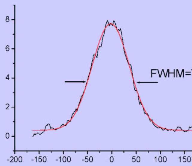
40 The excitonic peak appears without collection lens Sample TEC2, bunch of 24 optical fibres E= 9700 ev 1.0 with collection lens - BM08 without collection lens - BM Intensity (a.u./s) Wavelength (nm)

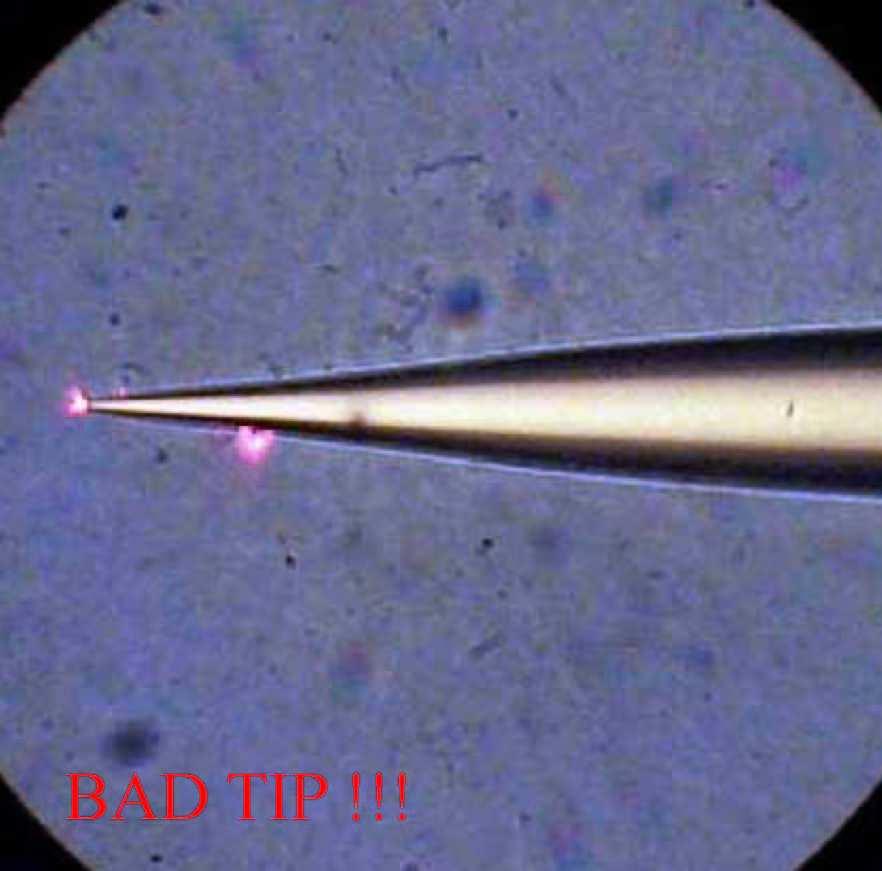
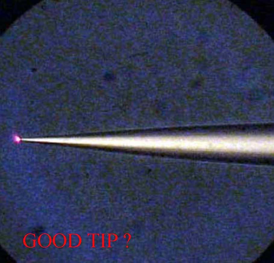
41 Goniometer characterisation Bad tip Intensity (µv) Angle (degree) Good tip Intensity (µv) 76.6 Angle (degree)
42 Radiation damage of the tip Phosphor luminescence spectra 1. directly measured 2. through unirradiated fiber 3. through X-rays irradiated fiber (10 hours)
 and quantum dots buried under Si layer (down).")
43 Promising results Luminescence distribution under X-rays for an uniform sample (up) and quantum dots buried under Si layer (down). The scanned surface is 5 µm x 5 µm

44
45 Three techniques/setup 1. XAS-STM STM mode photoelectrons emitted under X-ray irradiation collected by the STM tip 2. XAS-AFM AFM mode charge changes induced by X-rays are detected by the AFM tip 3. XAS-SNOM SNOM mode X-ray Excited Optical Luminescence (XEOL) is detected through the optical fiber of a SNOM Two kinds of measurements 1. Conventional scanning for 3D-mapping with element specific contrast 2. Probe fixed at a single point on the sample, X-ray energy tuned across the absorption edge
Microscopic Structures
 Microscopic Structures Image Analysis Metal, 3D Image (Red-Green) The microscopic methods range from dark field / bright field microscopy through polarisation- and inverse microscopy to techniques like
attosnom I: Topography and Force Images NANOSCOPY APPLICATION NOTE M06 RELATED PRODUCTS G
 APPLICATION NOTE M06 attosnom I: Topography and Force Images Scanning near-field optical microscopy is the outstanding technique to simultaneously measure the topography and the optical contrast of a sample.
attocfm I for Surface Quality Inspection NANOSCOPY APPLICATION NOTE M01 RELATED PRODUCTS G
 APPLICATION NOTE M01 attocfm I for Surface Quality Inspection Confocal microscopes work by scanning a tiny light spot on a sample and by measuring the scattered light in the illuminated volume. First,
Integrated into Nanowire Waveguides
 Supporting Information Widely Tunable Distributed Bragg Reflectors Integrated into Nanowire Waveguides Anthony Fu, 1,3 Hanwei Gao, 1,3,4 Petar Petrov, 1, Peidong Yang 1,2,3* 1 Department of Chemistry,
Design, Fabrication and Characterization of Very Small Aperture Lasers
 372 Progress In Electromagnetics Research Symposium 2005, Hangzhou, China, August 22-26 Design, Fabrication and Characterization of Very Small Aperture Lasers Jiying Xu, Jia Wang, and Qian Tian Tsinghua
Fabrication of Probes for High Resolution Optical Microscopy
 Fabrication of Probes for High Resolution Optical Microscopy Physics 564 Applied Optics Professor Andrès La Rosa David Logan May 27, 2010 Abstract Near Field Scanning Optical Microscopy (NSOM) is a technique
NSOM (SNOM) Overview
 Overview") NSOM (SNOM) Overview The limits of far field imaging In the early 1870s, Ernst Abbe formulated a rigorous criterion for being able to resolve two objects in a light microscope: d > ë / (2sinè) where d
NSOM (SNOM) Overview The limits of far field imaging In the early 1870s, Ernst Abbe formulated a rigorous criterion for being able to resolve two objects in a light microscope: d > ë / (2sinè) where d
:... resolution is about 1.4 μm, assumed an excitation wavelength of 633 nm and a numerical aperture of 0.65 at 633 nm.
 PAGE 30 & 2008 2007 PRODUCT CATALOG Confocal Microscopy - CFM fundamentals :... Over the years, confocal microscopy has become the method of choice for obtaining clear, three-dimensional optical images
Analytical analysis of modulated signal in apertureless scanning near-field optical microscopy C. H. Chuang and Y. L. Lo *
 Research Express@NCKU Volume 5 Issue 10 - October 3, 2008 [ http://research.ncku.edu.tw/re/articles/e/20081003/2.html ] Analytical analysis of modulated signal in apertureless scanning near-field optical
photolithographic techniques (1). Molybdenum electrodes (50 nm thick) are deposited by
. Molybdenum electrodes (50 nm thick) are deposited by") Supporting online material Materials and Methods Single-walled carbon nanotube (SWNT) devices are fabricated using standard photolithographic techniques (1). Molybdenum electrodes (50 nm thick) are deposited
Supporting online material Materials and Methods Single-walled carbon nanotube (SWNT) devices are fabricated using standard photolithographic techniques (1). Molybdenum electrodes (50 nm thick) are deposited
Nano Scale Optics with Nearfield Scanning Optical Microscopy (NSOM)
") Nano Scale Optics with Nearfield Scanning Optical Microscopy (NSOM) Presentation Overview Motivation for nearfield optics Introduction to NSOM What is NSOM today? What can you do with NSOM? November 2,
Nano Scale Optics with Nearfield Scanning Optical Microscopy (NSOM) Presentation Overview Motivation for nearfield optics Introduction to NSOM What is NSOM today? What can you do with NSOM? November 2,
- Near Field Scanning Optical Microscopy - Electrostatic Force Microscopy - Magnetic Force Microscopy
 - Near Field Scanning Optical Microscopy - Electrostatic Force Microscopy - Magnetic Force Microscopy Yongho Seo Near-field Photonics Group Leader Wonho Jhe Director School of Physics and Center for Near-field
SUPPLEMENTARY INFORMATION
 SUPPLEMENTARY INFORMATION Supplementary Information Real-space imaging of transient carrier dynamics by nanoscale pump-probe microscopy Yasuhiko Terada, Shoji Yoshida, Osamu Takeuchi, and Hidemi Shigekawa*
RECENTLY, using near-field scanning optical
 1 2 1 2 Theoretical and Experimental Study of Near-Field Beam Properties of High Power Laser Diodes W. D. Herzog, G. Ulu, B. B. Goldberg, and G. H. Vander Rhodes, M. S. Ünlü L. Brovelli, C. Harder Abstract
SUPPLEMENTARY INFORMATION
 Room-temperature continuous-wave electrically injected InGaN-based laser directly grown on Si Authors: Yi Sun 1,2, Kun Zhou 1, Qian Sun 1 *, Jianping Liu 1, Meixin Feng 1, Zengcheng Li 1, Yu Zhou 1, Liqun
Near-field Optical Microscopy
 Near-field Optical Microscopy R. Fernandez, X. Wang, N. Li, K. Parker, and A. La Rosa Physics Department Portland State University Portland, Oregon Near-Field SPIE Optics Microscopy East 2005 Group PSU
Study of shear force as a distance regulation mechanism for scanning near-field optical microscopy
 Study of shear force as a distance regulation mechanism for scanning near-field optical microscopy C. Durkan a) and I. V. Shvets Department of Physics, Trinity College Dublin, Ireland Received 31 May 1995;
PH880 Topics in Physics
 PH880 Topics in Physics Modern Optical Imaging (Fall 2010) Overview of week 12 Monday: FRET Wednesday: NSOM Förster resonance energy transfer (FRET) Fluorescence emission i FRET Donor Acceptor wikipedia
Diamond X-ray Rocking Curve and Topograph Measurements at CHESS
 Diamond X-ray Rocking Curve and Topograph Measurements at CHESS G. Yang 1, R.T. Jones 2, F. Klein 3 1 Department of Physics and Astronomy, University of Glasgow, Glasgow, UK G12 8QQ. 2 University of Connecticut
A Project Report Submitted to the Faculty of the Graduate School of the University of Minnesota By
 Observation and Manipulation of Gold Clusters with Scanning Tunneling Microscopy A Project Report Submitted to the Faculty of the Graduate School of the University of Minnesota By Dogukan Deniz In Partial
Nanoscale Systems for Opto-Electronics
 Nanoscale Systems for Opto-Electronics 675 PL intensity [arb. units] 700 Wavelength [nm] 650 625 600 5µm 1.80 1.85 1.90 1.95 Energy [ev] 2.00 2.05 1 Nanoscale Systems for Opto-Electronics Lecture 5 Interaction
RANDY W. ALKIRE, GEROLD ROSENBAUM AND GWYNDAF EVANS
 S-94,316 PATENTS-US-A96698 BEAM POSITION MONITOR RANDY W. ALKIRE, GEROLD ROSENBAUM AND GWYNDAF EVANS CONTRACTUAL ORIGIN OF THE INVENTION The United States Government has rights in this invention pursuant
Supplementary Information
 Supplementary Information For Nearly Lattice Matched All Wurtzite CdSe/ZnTe Type II Core-Shell Nanowires with Epitaxial Interfaces for Photovoltaics Kai Wang, Satish C. Rai,Jason Marmon, Jiajun Chen, Kun
Impact of the light coupling on the sensing properties of photonic crystal cavity modes Kumar Saurav* a,b, Nicolas Le Thomas a,b,
 Impact of the light coupling on the sensing properties of photonic crystal cavity modes Kumar Saurav* a,b, Nicolas Le Thomas a,b, a Photonics Research Group, Ghent University-imec, Technologiepark-Zwijnaarde
Lecture 20: Optical Tools for MEMS Imaging
 MECH 466 Microelectromechanical Systems University of Victoria Dept. of Mechanical Engineering Lecture 20: Optical Tools for MEMS Imaging 1 Overview Optical Microscopes Video Microscopes Scanning Electron
Applications of Steady-state Multichannel Spectroscopy in the Visible and NIR Spectral Region
 Feature Article JY Division I nformation Optical Spectroscopy Applications of Steady-state Multichannel Spectroscopy in the Visible and NIR Spectral Region Raymond Pini, Salvatore Atzeni Abstract Multichannel
Add CLUE to your SEM. High-efficiency CL signal-collection. Designed for your SEM and application. Maintains original SEM functionality
 Add CLUE to your SEM Designed for your SEM and application The CLUE family offers dedicated CL systems for imaging and spectroscopic analysis suitable for most SEMs. In addition, when combined with other
ELECTRON MICROSCOPY AN OVERVIEW
 ELECTRON MICROSCOPY AN OVERVIEW Anjali Priya 1, Abhishek Singh 2, Nikhil Anand Srivastava 3 1,2,3 Department of Electrical & Instrumentation, Sant Longowal Institute of Engg. & Technology, Sangrur, India.
Lithography. 3 rd. lecture: introduction. Prof. Yosi Shacham-Diamand. Fall 2004
 Lithography 3 rd lecture: introduction Prof. Yosi Shacham-Diamand Fall 2004 1 List of content Fundamental principles Characteristics parameters Exposure systems 2 Fundamental principles Aerial Image Exposure
k λ NA Resolution of optical systems depends on the wavelength visible light λ = 500 nm Extreme ultra-violet and soft x-ray light λ = 1-50 nm
 Resolution of optical systems depends on the wavelength visible light λ = 500 nm Spatial Resolution = k λ NA EUV and SXR microscopy can potentially resolve full-field images with 10-100x smaller features
VCSELs With Enhanced Single-Mode Power and Stabilized Polarization for Oxygen Sensing
 VCSELs With Enhanced Single-Mode Power and Stabilized Polarization for Oxygen Sensing Fernando Rinaldi and Johannes Michael Ostermann Vertical-cavity surface-emitting lasers (VCSELs) with single-mode,
Observation of X-rays generated by relativistic electrons in waveguide target mounted inside a betatron
 Observation of X-rays generated by relativistic electrons in waveguide target mounted inside a betatron V.V.Kaplin (1), V.V.Sohoreva (1), S.R.Uglov (1), O.F.Bulaev (2), A.A.Voronin (2), M.Piestrup (3),
ABSTRACT 1. INTRODUCTION
 Reflectance Fabry-Perot modulator utilizing electro-optic ZnO thin film Vikash Gulia* and Sanjeev Kumar Department of Physics and Astrophysics, University of Delhi, Delhi-117, India. *E-mail: vikasgulia222@rediffmail.com
First test experiments with FMB- Oxford direct drive DCM at the Sirius beamline of Synchrotron SOLEIL
 First test experiments with FMB- Oxford direct drive DCM at the Sirius beamline of Synchrotron SOLEIL Ciatto G., Moreno T., Aubert N., Feret P., Fontaine P. Synchrotron SOLEIL, L'Orme des Merisiers, Saint-Aubin,
SYNTHESIS AND CHARACTERIZATION OF II-IV GROUP AND SILICON RELATED NANOMATERIALS
 SYNTHESIS AND CHARACTERIZATION OF II-IV GROUP AND SILICON RELATED NANOMATERIALS ISMATHULLAKHAN SHAFIQ MASTER OF PHILOSOPHY CITY UNIVERSITY OF HONG KONG FEBRUARY 2008 CITY UNIVERSITY OF HONG KONG 香港城市大學
Today s Outline - January 25, C. Segre (IIT) PHYS Spring 2018 January 25, / 26
 PHYS Spring 2018 January 25, / 26") Today s Outline - January 25, 2018 C. Segre (IIT) PHYS 570 - Spring 2018 January 25, 2018 1 / 26 Today s Outline - January 25, 2018 HW #2 C. Segre (IIT) PHYS 570 - Spring 2018 January 25, 2018 1 / 26 Today
Today s Outline - January 25, 2018 C. Segre (IIT) PHYS 570 - Spring 2018 January 25, 2018 1 / 26 Today s Outline - January 25, 2018 HW #2 C. Segre (IIT) PHYS 570 - Spring 2018 January 25, 2018 1 / 26 Today
Introduction of New Products
 Field Emission Electron Microscope JEM-3100F For evaluation of materials in the fields of nanoscience and nanomaterials science, TEM is required to provide resolution and analytical capabilities that can
Administrative details:
 Administrative details: Anything from your side? www.photonics.ethz.ch 1 What are we actually doing here? Optical imaging: Focusing by a lens Angular spectrum Paraxial approximation Gaussian beams Method
Photon Diagnostics. FLASH User Workshop 08.
 Photon Diagnostics FLASH User Workshop 08 Kai.Tiedtke@desy.de Outline What kind of diagnostic tools do user need to make efficient use of FLASH? intensity (New GMD) beam position intensity profile on the
Angle-resolved cathodoluminescence spectroscopy
 Angle-resolved cathodoluminescence spectroscopy Toon Coenen, Ernst Jan R. Vesseur, and Albert Polman Center for Nanophotonics, FOM Institute AMOLF Science Park 104, 1098 XG Amsterdam, The Netherlands Abstract
Nano-structured superconducting single-photon detector
 Nano-structured superconducting single-photon detector G. Gol'tsman *a, A. Korneev a,v. Izbenko a, K. Smirnov a, P. Kouminov a, B. Voronov a, A. Verevkin b, J. Zhang b, A. Pearlman b, W. Slysz b, and R.
Measurement of Microscopic Three-dimensional Profiles with High Accuracy and Simple Operation
 238 Hitachi Review Vol. 65 (2016), No. 7 Featured Articles Measurement of Microscopic Three-dimensional Profiles with High Accuracy and Simple Operation AFM5500M Scanning Probe Microscope Satoshi Hasumura
Nd:YSO resonator array Transmission spectrum (a. u.) Supplementary Figure 1. An array of nano-beam resonators fabricated in Nd:YSO.
 Supplementary Figure 1. An array of nano-beam resonators fabricated in Nd:YSO.") a Nd:YSO resonator array µm Transmission spectrum (a. u.) b 4 F3/2-4I9/2 25 2 5 5 875 88 λ(nm) 885 Supplementary Figure. An array of nano-beam resonators fabricated in Nd:YSO. (a) Scanning electron microscope
a Nd:YSO resonator array µm Transmission spectrum (a. u.) b 4 F3/2-4I9/2 25 2 5 5 875 88 λ(nm) 885 Supplementary Figure. An array of nano-beam resonators fabricated in Nd:YSO. (a) Scanning electron microscope
GaAs polytype quantum dots
 GaAs polytype quantum dots Vilgailė Dagytė, Andreas Jönsson and Andrea Troian December 17, 2014 1 Introduction An issue that has haunted nanowire growth since it s infancy is the difficulty of growing
Photonic Crystal Slot Waveguide Spectrometer for Detection of Methane
 Photonic Crystal Slot Waveguide Spectrometer for Detection of Methane Swapnajit Chakravarty 1, Wei-Cheng Lai 2, Xiaolong (Alan) Wang 1, Che-Yun Lin 2, Ray T. Chen 1,2 1 Omega Optics, 10306 Sausalito Drive,
Examination Optoelectronic Communication Technology. April 11, Name: Student ID number: OCT1 1: OCT 2: OCT 3: OCT 4: Total: Grade:
 Examination Optoelectronic Communication Technology April, 26 Name: Student ID number: OCT : OCT 2: OCT 3: OCT 4: Total: Grade: Declaration of Consent I hereby agree to have my exam results published on
Heisenberg) relation applied to space and transverse wavevector
 relation applied to space and transverse wavevector") 2. Optical Microscopy 2.1 Principles A microscope is in principle nothing else than a simple lens system for magnifying small objects. The first lens, called the objective, has a short focal length (a
2. Optical Microscopy 2.1 Principles A microscope is in principle nothing else than a simple lens system for magnifying small objects. The first lens, called the objective, has a short focal length (a
Femtosecond laser microfabrication in. Prof. Dr. Cleber R. Mendonca
 Femtosecond laser microfabrication in polymers Prof. Dr. Cleber R. Mendonca laser microfabrication focus laser beam on material s surface laser microfabrication laser microfabrication laser microfabrication
Bandpass Edge Dichroic Notch & More
 Edmund Optics BROCHURE Filters COPYRIGHT 217 EDMUND OPTICS, INC. ALL RIGHTS RESERVED 1/17 Bandpass Edge Dichroic Notch & More Contact us for a Stock or Custom Quote Today! USA: +1-856-547-3488 EUROPE:
Nanowires for Quantum Optics
 Nanowires for Quantum Optics N. Akopian 1, E. Bakkers 1, J.C. Harmand 2, R. Heeres 1, M. v Kouwen 1, G. Patriarche 2, M. E. Reimer 1, M. v Weert 1, L. Kouwenhoven 1, V. Zwiller 1 1 Quantum Transport, Kavli
ANALYTICAL MICRO X-RAY FLUORESCENCE SPECTROMETER
 Copyright(c)JCPDS-International Centre for Diffraction Data 2001,Advances in X-ray Analysis,Vol.44 325 ANALYTICAL MICRO X-RAY FLUORESCENCE SPECTROMETER ABSTRACT William Chang, Jonathan Kerner, and Edward
High-Resolution Bubble Printing of Quantum Dots
 SUPPORTING INFORMATION High-Resolution Bubble Printing of Quantum Dots Bharath Bangalore Rajeeva 1, Linhan Lin 1, Evan P. Perillo 2, Xiaolei Peng 1, William W. Yu 3, Andrew K. Dunn 2, Yuebing Zheng 1,*
Oxidation of hydrogen-passivated silicon surfaces by scanning near-field optical lithography using uncoated and aluminum-coated fiber probes
 Downloaded from orbit.dtu.dk on: Dec 07, 2018 Oxidation of hydrogen-passivated silicon surfaces by scanning near-field optical lithography using uncoated and aluminum-coated fiber probes Madsen, Steen;
Human Retina. Sharp Spot: Fovea Blind Spot: Optic Nerve
 I am Watching YOU!! Human Retina Sharp Spot: Fovea Blind Spot: Optic Nerve Human Vision Optical Antennae: Rods & Cones Rods: Intensity Cones: Color Energy of Light 6 10 ev 10 ev 4 1 2eV 40eV KeV MeV Energy
Waveguiding in PMMA photonic crystals
 ROMANIAN JOURNAL OF INFORMATION SCIENCE AND TECHNOLOGY Volume 12, Number 3, 2009, 308 316 Waveguiding in PMMA photonic crystals Daniela DRAGOMAN 1, Adrian DINESCU 2, Raluca MÜLLER2, Cristian KUSKO 2, Alex.
*Corresponding author.
 Supporting Information for: Ligand-Free, Quantum-Confined Cs 2 SnI 6 Perovskite Nanocrystals Dmitriy S. Dolzhnikov, Chen Wang, Yadong Xu, Mercouri G. Kanatzidis, and Emily A. Weiss * Department of Chemistry,
Chapter 17: Wave Optics. What is Light? The Models of Light 1/11/13
 Chapter 17: Wave Optics Key Terms Wave model Ray model Diffraction Refraction Fringe spacing Diffraction grating Thin-film interference What is Light? Light is the chameleon of the physical world. Under
Nanonics Systems are the Only SPMs that Allow for On-line Integration with Standard MicroRaman Geometries
 Nanonics Systems are the Only SPMs that Allow for On-line Integration with Standard MicroRaman Geometries 2002 Photonics Circle of Excellence Award PLC Ltd, England, a premier provider of Raman microspectral
Mode analysis of Oxide-Confined VCSELs using near-far field approaches
 Annual report 998, Dept. of Optoelectronics, University of Ulm Mode analysis of Oxide-Confined VCSELs using near-far field approaches Safwat William Zaki Mahmoud We analyze the transverse mode structure
Improving the Collection Efficiency of Raman Scattering
 PERFORMANCE Unparalleled signal-to-noise ratio with diffraction-limited spectral and imaging resolution Deep-cooled CCD with excelon sensor technology Aberration-free optical design for uniform high resolution
CHAPTER 9 POSITION SENSITIVE PHOTOMULTIPLIER TUBES
 CHAPTER 9 POSITION SENSITIVE PHOTOMULTIPLIER TUBES The current multiplication mechanism offered by dynodes makes photomultiplier tubes ideal for low-light-level measurement. As explained earlier, there
Lesson 2 Diffractometers
 Lesson 2 Diffractometers Nicola Döbelin RMS Foundation, Bettlach, Switzerland January 14 16, 2015, Bern, Switzerland Repetition: Generation of X-rays / Diffraction SEM: BSE detector, BSED / SAED detector
Contents. Nano-2. Nano-2. Nanoscience II: Nanowires. 2. Growth of nanowires. 1. Nanowire concepts Nano-2. Nano-2
 Contents Nanoscience II: Nanowires Kai Nordlund 17.11.2010 Faculty of Science Department of Physics Division of Materials Physics 1. Introduction: nanowire concepts 2. Growth of nanowires 1. Spontaneous
EUV and Soft X-Ray Optics
 David Attwood University of California, Berkeley Cheiron School September 2012 SPring-8 1 The short wavelength region of the electromagnetic spectrum n = 1 + i,
Supplementary Information
 Supplementary Information Atomically flat single crystalline gold nanostructures for plasmonic nanocircuitry Jer Shing Huang 1,*, Victor Callegari 2, Peter Geisler 1, Christoph Brüning 1, Johannes Kern
Absorption: in an OF, the loss of Optical power, resulting from conversion of that power into heat.
 Absorption: in an OF, the loss of Optical power, resulting from conversion of that power into heat. Scattering: The changes in direction of light confined within an OF, occurring due to imperfection in
Nanopatterning using NSOM probes integrated with high transmission nanoscale bowtie aperture
 Nanopatterning using NSOM probes integrated with high transmission nanoscale bowtie aperture Nicholas Murphy-DuBay, Liang Wang, Edward C. Kinzel, Sreemanth M. V. Uppuluri, and X. Xu * School of Mechanical
Luminous Equivalent of Radiation
 Intensity vs λ Luminous Equivalent of Radiation When the spectral power (p(λ) for GaP-ZnO diode has a peak at 0.69µm) is combined with the eye-sensitivity curve a peak response at 0.65µm is obtained with
Advances in X-Ray Scintillator Technology Roger D. Durst Bruker AXS Inc.
 Advances in X-Ray Scintillator Technology Roger D. Durst Inc. Acknowledgements T. Thorson, Y. Diawara, E. Westbrook, MBC J. Morse, ESRF C. Summers, Georgia Tech/PTCE B. Wagner, Georgia Tech/PTCE V. Valdna,
Introduction Fundamentals of laser Types of lasers Semiconductor lasers
 ECE 5368 Introduction Fundamentals of laser Types of lasers Semiconductor lasers Introduction Fundamentals of laser Types of lasers Semiconductor lasers How many types of lasers? Many many depending on
Devices Imaged with Near-eld Scanning Optical Microscopy. G. H. Vander Rhodes, M. S. Unlu, and B. B. Goldberg. J. M. Pomeroy
 Internal Spatial Modes of One Dimensional Photonic Band Gap Devices Imaged with Near-eld Scanning Optical Microscopy G. H. Vander Rhodes, M. S. Unlu, and B. B. Goldberg Departments of Physics and Electrical
Optical behavior. Reading assignment. Topic 10
 Reading assignment Optical behavior Topic 10 Askeland and Phule, The Science and Engineering of Materials, 4 th Ed.,Ch. 0. Shackelford, Materials Science for Engineers, 6 th Ed., Ch. 16. Chung, Composite
Supplementary Materials for
 advances.sciencemag.org/cgi/content/full/3/10/eaao4204/dc1 Supplementary Materials for Enhanced mobility CsPbI3 quantum dot arrays for record-efficiency, high-voltage photovoltaic cells Erin M. Sanehira,
NIST EUVL Metrology Programs
 NIST EUVL Metrology Programs S.Grantham, C. Tarrio, R.E. Vest, Y. Barad, S. Kulin, K. Liu and T.B. Lucatorto National Institute of Standards and Technology (NIST) Gaithersburg, MD USA L. Klebanoff and
Lecture 19 Optical Characterization 1
 Lecture 19 Optical Characterization 1 1/60 Announcements Homework 5/6: Is online now. Due Wednesday May 30th at 10:00am. I will return it the following Wednesday (6 th June). Homework 6/6: Will be online
Supporting Information: Plasmonic and Silicon Photonic Waveguides
 Supporting Information: Efficient Coupling between Dielectric-Loaded Plasmonic and Silicon Photonic Waveguides Ryan M. Briggs, *, Jonathan Grandidier, Stanley P. Burgos, Eyal Feigenbaum, and Harry A. Atwater,
Scanning electron microscope
 Scanning electron microscope 5 th CEMM workshop Maja Koblar, Sc. Eng. Physics Outline The basic principle? What is an electron? Parts of the SEM Electron gun Electromagnetic lenses Apertures Detectors
Investigation of the Near-field Distribution at Novel Nanometric Aperture Laser
 Investigation of the Near-field Distribution at Novel Nanometric Aperture Laser Tiejun Xu, Jia Wang, Liqun Sun, Jiying Xu, Qian Tian Presented at the th International Conference on Electronic Materials
PHY 431 Homework Set #5 Due Nov. 20 at the start of class
 PHY 431 Homework Set #5 Due Nov. 0 at the start of class 1) Newton s rings (10%) The radius of curvature of the convex surface of a plano-convex lens is 30 cm. The lens is placed with its convex side down
Narrowing spectral width of green LED by GMR structure to expand color mixing field
 Narrowing spectral width of green LED by GMR structure to expand color mixing field S. H. Tu 1, Y. C. Lee 2, C. L. Hsu 1, W. P. Lin 1, M. L. Wu 1, T. S. Yang 1, J. Y. Chang 1 1. Department of Optical and
Outline: Introduction: What is SPM, history STM AFM Image treatment Advanced SPM techniques Applications in semiconductor research and industry
 1 Outline: Introduction: What is SPM, history STM AFM Image treatment Advanced SPM techniques Applications in semiconductor research and industry 2 Back to our solutions: The main problem: How to get nm
Medical Imaging. X-rays, CT/CAT scans, Ultrasound, Magnetic Resonance Imaging
 Medical Imaging X-rays, CT/CAT scans, Ultrasound, Magnetic Resonance Imaging From: Physics for the IB Diploma Coursebook 6th Edition by Tsokos, Hoeben and Headlee And Higher Level Physics 2 nd Edition
Microprobe-enabled Terahertz sensing applications
 Microprobe-enabled Terahertz sensing applications World of Photonics, Laser 2015, Munich Protemics GmbH Aachen, Germany Terahertz microprobing technology: Taking advantage of Terahertz range benefits without
A novel tunable diode laser using volume holographic gratings
 A novel tunable diode laser using volume holographic gratings Christophe Moser *, Lawrence Ho and Frank Havermeyer Ondax, Inc. 85 E. Duarte Road, Monrovia, CA 9116, USA ABSTRACT We have developed a self-aligned
Superconducting Nanowire Single Photon Detector (SNSPD) integrated with optical circuits
 integrated with optical circuits") Superconducting Nanowire Single Photon Detector (SNSPD) integrated with optical circuits Marcello Graziosi, ESR 3 within PICQUE (Marie Curie ITN project) and PhD student marcello.graziosi@ifn.cnr.it Istituto
Superconducting Nanowire Single Photon Detector (SNSPD) integrated with optical circuits Marcello Graziosi, ESR 3 within PICQUE (Marie Curie ITN project) and PhD student marcello.graziosi@ifn.cnr.it Istituto
OPTICAL SENSORS-CONSTRUCTION ALTERNATIVES
 OPTICAL SENSORS-CONSTRUCTION ALTERNATIVES Mariana ENACHE, Cristina ŢUINEA BOBE Universitatea Valahia Târgovişte, Facultatea Ştiinta si Ingineria Materialelor, B-dul Regele Carol I, Nr.2, 0200, Târgovişte,
High Performance Thin Film Optical Coatings Technical Reference Document 09/13. Coatings Capabilities. Heat Control - Hot Mirror Filters
 Heat Control - Hot Mirror Filters A hot mirror is in essence a thin film coating applied to substrates in an effort to reflect infra-red radiation either as a means to harness the reflected wavelengths
CHIRPED FIBER BRAGG GRATING (CFBG) BY ETCHING TECHNIQUE FOR SIMULTANEOUS TEMPERATURE AND REFRACTIVE INDEX SENSING
 BY ETCHING TECHNIQUE FOR SIMULTANEOUS TEMPERATURE AND REFRACTIVE INDEX SENSING") CHIRPED FIBER BRAGG GRATING (CFBG) BY ETCHING TECHNIQUE FOR SIMULTANEOUS TEMPERATURE AND REFRACTIVE INDEX SENSING Siti Aisyah bt. Ibrahim and Chong Wu Yi Photonics Research Center Department of Physics,
CHIRPED FIBER BRAGG GRATING (CFBG) BY ETCHING TECHNIQUE FOR SIMULTANEOUS TEMPERATURE AND REFRACTIVE INDEX SENSING Siti Aisyah bt. Ibrahim and Chong Wu Yi Photonics Research Center Department of Physics,
Components of Optical Instruments
 Components of Optical Instruments General Design of Optical Instruments Sources of Radiation Wavelength Selectors (Filters, Monochromators, Interferometers) Sample Containers Radiation Transducers (Detectors)
Scanning Tunneling Microscopy
 EMSE-515 02 Scanning Tunneling Microscopy EMSE-515 F. Ernst 1 Scanning Tunneling Microscope: Working Principle 2 Scanning Tunneling Microscope: Construction Principle 1 sample 2 sample holder 3 clamps
with valuable information only accessible with optical contrast. One should look at it as a complementary tool with some room for improvement.
 Introduction Optical microscopy has come a long way from Zacharias Jansen s first microscope at the end of the 16th century to today s highly developed microscopes. A number of different contrast mechanisms
Scanning Electron Microscopy Basics and Applications
 Scanning Electron Microscopy Basics and Applications Dr. Julia Deuschle Stuttgart Center for Electron Microscopy MPI for Solid State Research Room: 1E15, phone: 0711/ 689-1193 email: j.deuschle@fkf.mpg.de
Resolution. Diffraction from apertures limits resolution. Rayleigh criterion θ Rayleigh = 1.22 λ/d 1 peak at 2 nd minimum. θ f D
 Microscopy Outline 1. Resolution and Simple Optical Microscope 2. Contrast enhancement: Dark field, Fluorescence (Chelsea & Peter), Phase Contrast, DIC 3. Newer Methods: Scanning Tunneling microscopy (STM),
Chapter 1. Basic Electron Optics (Lecture 2)
") Chapter 1. Basic Electron Optics (Lecture 2) Basic concepts of microscope (Cont ) Fundamental properties of electrons Electron Scattering Instrumentation Basic conceptions of microscope (Cont ) Ray diagram
Chapter 1. Basic Electron Optics (Lecture 2) Basic concepts of microscope (Cont ) Fundamental properties of electrons Electron Scattering Instrumentation Basic conceptions of microscope (Cont ) Ray diagram
X-ray generation by femtosecond laser pulses and its application to soft X-ray imaging microscope
 X-ray generation by femtosecond laser pulses and its application to soft X-ray imaging microscope Kenichi Ikeda 1, Hideyuki Kotaki 1 ' 2 and Kazuhisa Nakajima 1 ' 2 ' 3 1 Graduate University for Advanced
plasmonic nanoblock pair
 Nanostructured potential of optical trapping using a plasmonic nanoblock pair Yoshito Tanaka, Shogo Kaneda and Keiji Sasaki* Research Institute for Electronic Science, Hokkaido University, Sapporo 1-2,
3D simulations of the experimental signal measured in near-field optical microscopy
 Journal of Microscopy, Vol. 194, Pt 2/3, May/June 1999, pp. 235 239. Received 6 December 1998; accepted 4 February 1999 3D simulations of the experimental signal measured in near-field optical microscopy
VISUAL PHYSICS ONLINE DEPTH STUDY: ELECTRON MICROSCOPES
 VISUAL PHYSICS ONLINE DEPTH STUDY: ELECTRON MICROSCOPES Shortly after the experimental confirmation of the wave properties of the electron, it was suggested that the electron could be used to examine objects
Laser stabilization and frequency modulation for trapped-ion experiments
 Laser stabilization and frequency modulation for trapped-ion experiments Michael Matter Supervisor: Florian Leupold Semester project at Trapped Ion Quantum Information group July 16, 2014 Abstract A laser
Unit thickness. Unit area. σ = NΔX = ΔI / I 0
 Unit thickness I 0 ΔI I σ = ΔI I 0 NΔX = ΔI / I 0 NΔX Unit area Δx Average probability of reaction with atom for the incident photons at unit area with the thickness of Delta-X Atom number at unit area