Titelfoto. Advanced Laser Beam Shaping - for Optimized Process Results and Quality Inspection in the PV Production - Maja Thies.
|
|
|
- Gabriella Stokes
- 5 years ago
- Views:
Transcription

1 2010 LIMO Lissotschenko Mikrooptik GmbH Titelfoto Advanced Laser Beam Shaping - for Optimized Process Results and Quality Inspection in the PV Production - Maja Thies Photonics Key Technology for an Effective and Cost-Efficient PV Production 27 th September 2012

2 LIMO Solar Cell Solution - Overview Gaussian-to-top-hat conversion for laser direct patterning Multi-spot-generators for fast parallel processing Laser line generators for material properties engineering Off-axis illumination for inline quality control 2
3 LIMO Solar Cell Solution - Overview Gaussian-to-top-hat conversion for laser direct patterning Multi-spot-generators for fast parallel processing Laser line generators for material properties engineering Off-axis illumination for inline quality control 3


4 Beam Shaping Principle: Phase Shifting (for single mode lasers) Collimated Gaussian beam Free-form phase shifting element Generated Top-hat profile Simulation Measurement 4
![Overview g2t Converter Overview g2t converters Wavelength [nm] Top hat [mm] WD [mm] DOF [mm] 355 0.03 x 0.03 0.05 x 0.05 69 92 ±0.04 ±0.07 532 1.064 10.0 x 10.0 0.03 x 0.03 0.05 x 0.05 0.](/docs-images/83/88153514/images/5-2.jpg "05 x 0.05 10.0 x 10.0 0.5 x 0.5 204 71 96 147 190 46 ±8 ±0.05 ±0.30 ±0.40 ±10.0 ±0.20 2nd converter generation with increased depth of field 9.6 x 9.6 196 ±13 5")
5 Overview g2t Converter Overview g2t converters Wavelength [nm] Top hat [mm] WD [mm] DOF [mm] x x ±0.04 ± x x x x x x ±8 ±0.05 ±0.30 ±0.40 ±10.0 ±0.20 2nd converter generation with increased depth of field 9.6 x ±13 5


6 Laser Direct Patterning Gaussian Profile vs. Top Hat Profiles Steep edges Uniform patterning 6


7 Laser Direct Patterning Gaussian Profile vs. Top Hat Profiles Higher efficiency Energy content Increase of Efficiency 2D Profile Gauss Top-Hat Top Hat- Gauss FW90% 36% 68% +80% FW50% 74% 90% +20% Smooth edges, increased throughput 7
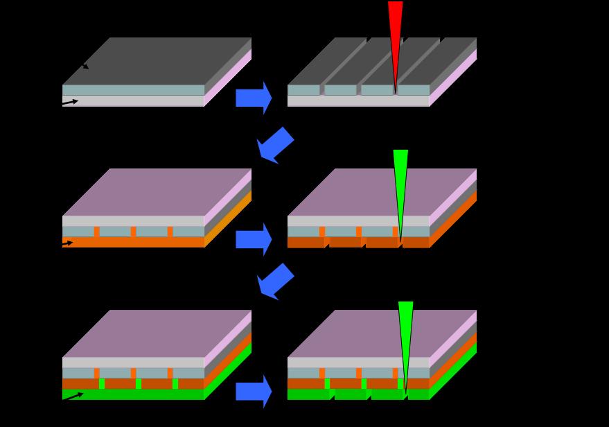

8 Laser Structuring of Thin Film Solar Cells 8


9 Patterning Examples SnO 2 Gaussian profile Top hat profile Polyimide Structuring Advantages Smooth edges Reduced heat affected zone, no delamination Precise thin film ablation, no damage of underlying material 9
10 LIMO g2t -Scan-System Single Mode Laser Attenuator Beam Expander g2t 30 mm Scanner XY-stage XY-stage g2tf-theta lens Specification ~ 200 mm Wavelength 532 nm Top hat size 50 µm Scan area 156 x156 mm² ~ 500 mm ~ 400 mm Advantages Top hat patterning High speed Precision Target 10


11 Laser Fired Contacts Local contacts through the passivation are created with single laser pulses contact energy threshold Energy high above the contact threshold induces damage to the Silicon substrate 11
12 LIMO Solar Cell Solution - Overview Gaussian-to-top-hat conversion for laser direct patterning Multi-Spot-generators for fast parallel processing Laser line generators for material properties engineering Off-axis illumination for inline quality control 12

13 LIMO Proprietary Technology NO quantization error NO scattering on the relief discontinuities NO surface defects HIGH damage threshold Efficiency > 95% HIGH homogeneity also coherent beam combining 13

 1 DOE Profile 0.5. 0 0 0.02 0.04 0.06 0.08 0.1 0.12 0.14 0.")
14 Z, um Kinoform Beam Splitters Romero, L.A., Dickey, F. M., "Theory of optimal beam splitting by phase gratings. I. One-dimensional gratings", J. Opt. Soc. Am. A, 24, (2007) 1 DOE Profile x, mm Quartz, Pitch 20 µm, λ = 1064 nm, inter-beam angle i = /Pitch = 53.2 mrad 14


15 Measurement Data: Power Distribution Inhomogeneity: ± 5% Total Efficiency: 95 ± 2 % Foto 2 15
16 LIMO Solar Cell Solution - Overview Gaussian-to-top-hat conversion for laser direct patterning Multi-spot-generators for fast parallel processing Laser line generators for material properties engineering Off-axis illumination for inline quality control 16


17 LIMO Line Laser Punctiform laser source Discontinous, multidirectional heat distribution L³ - Limo Line Laser Continous linear heat distribution Punctiform laser source L³ - Limo Line Laser 17


18 Crystallization of a-si Thin Films on Glass Using a Diode Laser Laser source 450W, 808 nm direct diode line beam 12 mm x 100 µm Material 200 nm a-si on glass Process First results (R&D) single scan at a scanning speed of 33 mm/s crystal grain size > 100 µm increased charge carrier mobility in the absorber layer reduced surface resistance (R sq ) Pictures: IPHT, Jena Foto 1 Foto 1 Foto µm 18
19 LIMO Solar Cell Solution - Overview Gaussian-to-top-hat conversion for laser direct patterning Multi-spot-generators for fast parallel processing Laser line generators for material properties engineering Off-axis illumination for inline quality control 19


20 Inline Quality Control Advantages of quality assurance by photoluminescence At various inline production steps possible Contactless and non-destructive Cost-efficient Fast, high throughput Technical Specifications of illumination source Top-Hat profile under an illumination angle of 35 Field size: > 156 x 156 mm² Power: variable Wavelength: 790 / 808 nm Inhomogeneity: (lmax-lmin)/(lmax+lmin) < 7.5 % 20


21 Asymmetric Homogenizers Give Best Uniformity Symmetric homogenizer Inhomogeneity ~ 25 % Asymmetric homogenizer Inhomogeneity < 7.5 % 21
 / (Imax+Imin) < 7.")
22 Line Laser for Scanning of the Solar Cell Technical specifications for laser line generator: Compactness Line dimensions: 165 mm x 3 mm Power: 40 W Wavelength: 790 / 808 nm Inhomogeneity: (lmax-imin) / (Imax+Imin) < 7.5 % Foto 2 22

")


23 Photoluminescence Results As cut wafers Solar cell (Courtesy of J. Haunschild, Fraunhofer ISE ) Good correlation between PL of as-cut wafers and solar cells Effective and cost-efficient inline analysis in solar cell production 23


24 LIMOs Application-Specific Optics Solutions Have the Following Advantages Very homogeneous light fields and spots Highest efficiency and throughput Superior manufacturing results Increased productivity and decreased cost per unit! Foto 1 Foto 1 Foto 1 24

25 2010 LIMO Lissotschenko Mikrooptik GmbH Titelfoto Thank you for your attention!
Generation of a Line Focus for Material Processing from an Array of High Power Diode Laser Bars R. Baettig, N. Lichtenstein, R. Brunner, J.
 Generation of a Line Focus for Material Processing from an Array of High Power Diode Laser Bars R. Baettig, N. Lichtenstein, R. Brunner, J. Müller, B. Valk, M. Kreijci, S. Weiss Overview This slidepack
Beam Shaping and Simultaneous Exposure by Diffractive Optical Element in Laser Plastic Welding
 Beam Shaping and Simultaneous Exposure by Diffractive Optical Element in Laser Plastic Welding AKL`12 9th May 2012 Dr. Daniel Vogler Page 1 Motivation: Quality and flexibility diffractive spot shaping
Practical Applications of Laser Technology for Semiconductor Electronics
 Practical Applications of Laser Technology for Semiconductor Electronics MOPA Single Pass Nanosecond Laser Applications for Semiconductor / Solar / MEMS & General Manufacturing Mark Brodsky US Application
Inline PL Imaging Techniques for Crystalline Silicon Cell Production. F. Korsós, Z. Kiss, Ch. Defranoux and S. Gaillard
 Inline PL Imaging Techniques for Crystalline Silicon Cell Production F. Korsós, Z. Kiss, Ch. Defranoux and S. Gaillard OUTLINE I. Categorization of PL imaging techniques II. PL imaging setups III. Inline
CREATING ROUND AND SQUARE FLATTOP LASER SPOTS IN MICROPROCESSING SYSTEMS WITH SCANNING OPTICS Paper M305
 CREATING ROUND AND SQUARE FLATTOP LASER SPOTS IN MICROPROCESSING SYSTEMS WITH SCANNING OPTICS Paper M305 Alexander Laskin, Vadim Laskin AdlOptica Optical Systems GmbH, Rudower Chaussee 29, 12489 Berlin,
Micro- and Nano-Technology... for Optics
 Micro- and Nano-Technology...... for Optics 3.2 Lithography U.D. Zeitner Fraunhofer Institut für Angewandte Optik und Feinmechanik Jena Printing on Stones Map of Munich Stone Print Contact Printing light
Point Autofocus Probe Surface Texture Measuring Instrument. PF-60 technical report
 Point Autofocus Probe Surface Texture Measuring Instrument PF-60 technical report ISO approved Mitaka measuring method for areal surface texture (ISO 25178-605) Document No, Title Published ISO 25178-6
Beam shaping imaging system for laser microprocessing with scanning optics
 Beam shaping imaging system for laser microprocessing with scanning optics Alexander Laskin a, Nerijus Šiaulys b, Gintas Šlekys b, Vadim Laskin a a AdlOptica GmbH, Rudower Chaussee 29, 12489 Berlin, Germany
Optical Components for Laser Applications. Günter Toesko - Laserseminar BLZ im Dezember
 Günter Toesko - Laserseminar BLZ im Dezember 2009 1 Aberrations An optical aberration is a distortion in the image formed by an optical system compared to the original. It can arise for a number of reasons
ARCoptix. Radial Polarization Converter. Arcoptix S.A Ch. Trois-portes Neuchâtel Switzerland Mail: Tel:
 ARCoptix Radial Polarization Converter Arcoptix S.A Ch. Trois-portes 18 2000 Neuchâtel Switzerland Mail: info@arcoptix.com Tel: ++41 32 731 04 66 Radially and azimuthally polarized beams generated by Liquid
Properties of Structured Light
 Properties of Structured Light Gaussian Beams Structured light sources using lasers as the illumination source are governed by theories of Gaussian beams. Unlike incoherent sources, coherent laser sources
Measurement of Surface Profile and Layer Cross-section with Wide Field of View and High Precision
 Hitachi Review Vol. 65 (2016), No. 7 243 Featured Articles Measurement of Surface Profile and Layer Cross-section with Wide Field of View and High Precision VS1000 Series Coherence Scanning Interferometer
attocfm I for Surface Quality Inspection NANOSCOPY APPLICATION NOTE M01 RELATED PRODUCTS G
 APPLICATION NOTE M01 attocfm I for Surface Quality Inspection Confocal microscopes work by scanning a tiny light spot on a sample and by measuring the scattered light in the illuminated volume. First,
Fastest high definition Raman imaging. Fastest Laser Raman Microscope RAMAN
 Fastest high definition Raman imaging Fastest Laser Raman Microscope RAMAN - 11 www.nanophoton.jp Observation A New Generation in Raman Observation RAMAN-11 developed by Nanophoton was newly created by
Near-field optical photomask repair with a femtosecond laser
 Journal of Microscopy, Vol. 194, Pt 2/3, May/June 1999, pp. 537 541. Received 6 December 1998; accepted 9 February 1999 Near-field optical photomask repair with a femtosecond laser K. LIEBERMAN, Y. SHANI,
White Paper: Modifying Laser Beams No Way Around It, So Here s How
 White Paper: Modifying Laser Beams No Way Around It, So Here s How By John McCauley, Product Specialist, Ophir Photonics There are many applications for lasers in the world today with even more on the
Diffractive Axicon application note
 Diffractive Axicon application note. Introduction 2. General definition 3. General specifications of Diffractive Axicons 4. Typical applications 5. Advantages of the Diffractive Axicon 6. Principle of
Beam Shaping in High-Power Laser Systems with Using Refractive Beam Shapers
 - 1 - Beam Shaping in High-Power Laser Systems with Using Refractive Beam Shapers Alexander Laskin, Vadim Laskin AdlOptica GmbH, Rudower Chaussee 29, 12489 Berlin, Germany ABSTRACT Beam Shaping of the
Rear Side Processing of Soda-Lime Glass Using DPSS Nanosecond Laser
 Lasers in Manufacturing Conference 215 Rear Side Processing of Soda-Lime Glass Using DPSS Nanosecond Laser Juozas Dudutis*, Paulius Gečys, Gediminas Račiukaitis Center for Physical Sciences and Technology,
Fast Laser Raman Microscope RAMAN
 Fast Laser Raman Microscope RAMAN - 11 www.nanophoton.jp Fast Raman Imaging A New Generation of Raman Microscope RAMAN-11 developed by Nanophoton was created by combining confocal laser microscope technology
Fast Laser Raman Microscope RAMAN
 Fast Laser Raman Microscope RAMAN - 11 www.nanophoton.jp Fast Raman Imaging A New Generation of Raman Microscope RAMAN-11 developed by Nanophoton was created by combining confocal laser microscope technology
Lithography. 3 rd. lecture: introduction. Prof. Yosi Shacham-Diamand. Fall 2004
 Lithography 3 rd lecture: introduction Prof. Yosi Shacham-Diamand Fall 2004 1 List of content Fundamental principles Characteristics parameters Exposure systems 2 Fundamental principles Aerial Image Exposure
Microprobe-enabled Terahertz sensing applications
 Microprobe-enabled Terahertz sensing applications World of Photonics, Laser 2015, Munich Protemics GmbH Aachen, Germany Terahertz microprobing technology: Taking advantage of Terahertz range benefits without
Application of EOlite Flexible Pulse Technology. Matt Rekow Yun Zhou Nicolas Falletto
 Application of EOlite Flexible Pulse Technology Matt Rekow Yun Zhou Nicolas Falletto 1 Topics Company Background What is a Flexible Pulse Laser? Why Tailored or Flexible Pulse? Application of Flexible
BEAM SHAPING OPTICS TO IMPROVE HOLOGRAPHIC AND INTERFEROMETRIC NANOMANUFACTURING TECHNIQUES Paper N405 ABSTRACT
 BEAM SHAPING OPTICS TO IMPROVE HOLOGRAPHIC AND INTERFEROMETRIC NANOMANUFACTURING TECHNIQUES Paper N5 Alexander Laskin, Vadim Laskin AdlOptica GmbH, Rudower Chaussee 9, 89 Berlin, Germany ABSTRACT Abstract
HCS 50W, 60W & 80W. Data Sheet. Housed Collimated High Power Laser Diode Bar
 HCS 50W, 60W & 80W Housed Collimated High Power Laser Diode Bar Features: The II-VI Laser Enterprise HCS series of hard soldered collimated laser diode bars offer superior optical beam parameters with
Wavelength Stabilization of HPDL Array Fast-Axis Collimation Optic with integrated VHG
 Wavelength Stabilization of HPDL Array Fast-Axis Collimation Optic with integrated VHG C. Schnitzler a, S. Hambuecker a, O. Ruebenach a, V. Sinhoff a, G. Steckman b, L. West b, C. Wessling c, D. Hoffmann
Diffuser / Homogenizer - diffractive optics
 Diffuser / Homogenizer - diffractive optics Introduction Homogenizer (HM) product line can be useful in many applications requiring a well-defined beam shape with a randomly-diffused intensity profile.
A process for, and optical performance of, a low cost Wire Grid Polarizer
 1.0 Introduction A process for, and optical performance of, a low cost Wire Grid Polarizer M.P.C.Watts, M. Little, E. Egan, A. Hochbaum, Chad Jones, S. Stephansen Agoura Technology Low angle shadowed deposition
Coherent PowerLine. High-Power Structured Light Pattern Generating Laser FEATURES
 Coherent PowerLine High-Power Structured Light Pattern Generating Laser Coherent s PowerLine structured light laser is a line generator developed for demanding industrial machine vision and scientific
UV EXCIMER LASER BEAM HOMOGENIZATION FOR MICROMACHINING APPLICATIONS
 Optics and Photonics Letters Vol. 4, No. 2 (2011) 75 81 c World Scientific Publishing Company DOI: 10.1142/S1793528811000226 UV EXCIMER LASER BEAM HOMOGENIZATION FOR MICROMACHINING APPLICATIONS ANDREW
Lasers Defect Correction in DRAM's Problem: very hard to make memory chips with no defects Memory chips have maximum density of devices Repeated
 Lasers Defect Correction in DRAM's Problem: very hard to make memory chips with no defects Memory chips have maximum density of devices Repeated structures all substitutable Create spare rows and columns
Applying of refractive beam shapers of circular symmetry to generate non-circular shapes of homogenized laser beams
 - 1 - Applying of refractive beam shapers of circular symmetry to generate non-circular shapes of homogenized laser beams Alexander Laskin a, Vadim Laskin b a MolTech GmbH, Rudower Chaussee 29-31, 12489
EE119 Introduction to Optical Engineering Spring 2003 Final Exam. Name:
 EE119 Introduction to Optical Engineering Spring 2003 Final Exam Name: SID: CLOSED BOOK. THREE 8 1/2 X 11 SHEETS OF NOTES, AND SCIENTIFIC POCKET CALCULATOR PERMITTED. TIME ALLOTTED: 180 MINUTES Fundamental
Optical Characterization and Defect Inspection for 3D Stacked IC Technology
 Minapad 2014, May 21 22th, Grenoble; France Optical Characterization and Defect Inspection for 3D Stacked IC Technology J.Ph.Piel, G.Fresquet, S.Perrot, Y.Randle, D.Lebellego, S.Petitgrand, G.Ribette FOGALE
Measurement of Microscopic Three-dimensional Profiles with High Accuracy and Simple Operation
 238 Hitachi Review Vol. 65 (2016), No. 7 Featured Articles Measurement of Microscopic Three-dimensional Profiles with High Accuracy and Simple Operation AFM5500M Scanning Probe Microscope Satoshi Hasumura
EUV Substrate and Blank Inspection
 EUV Substrate and Blank Inspection SEMATECH EUV Workshop 10/11/99 Steve Biellak KLA-Tencor RAPID Division *This work is partially funded by NIST-ATP project 98-06, Project Manager Purabi Mazumdar 1 EUV
Dr. Ralf Freiberger. TEMA GmbH / Mühlbauer Group
 Welcome to ADF&PCD Paris 2018 Inline Final Inspection of Aerosol Cans Dr. Ralf Freiberger TEMA GmbH / Mühlbauer Group Overview 1. Purpose 2. State of the Art: Integration in Line 3. New: Inspection at
Ultrafast Lasers with Radial and Azimuthal Polarizations for Highefficiency. Applications
 WP Ultrafast Lasers with Radial and Azimuthal Polarizations for Highefficiency Micro-machining Applications Beneficiaries Call Topic Objective ICT-2013.3.2 Photonics iii) Laser for Industrial processing
Optical Bus for Intra and Inter-chip Optical Interconnects
 Optical Bus for Intra and Inter-chip Optical Interconnects Xiaolong Wang Omega Optics Inc., Austin, TX Ray T. Chen University of Texas at Austin, Austin, TX Outline Perspective of Optical Backplane Bus
Spatial Light Modulators in Laser Microprocessing
 Spatial Light Modulators in Laser Microprocessing Grigory Lazarev HOLOEYE Photonics AG Berlin, Germany Workshop: APPOLO 04.11.2015, BFH Burgdorf SLMs Variety Today MEMS (one- or two dimensional) Piston-like
Criteria for Optical Systems: Optical Path Difference How do we determine the quality of a lens system? Several criteria used in optical design
 Criteria for Optical Systems: Optical Path Difference How do we determine the quality of a lens system? Several criteria used in optical design Computer Aided Design Several CAD tools use Ray Tracing (see
Supplementary Figure 1. GO thin film thickness characterization. The thickness of the prepared GO thin
 Supplementary Figure 1. GO thin film thickness characterization. The thickness of the prepared GO thin film is characterized by using an optical profiler (Bruker ContourGT InMotion). Inset: 3D optical
Will contain image distance after raytrace Will contain image height after raytrace
 Name: LASR 51 Final Exam May 29, 2002 Answer all questions. Module numbers are for guidance, some material is from class handouts. Exam ends at 8:20 pm. Ynu Raytracing The first questions refer to the
LITE /LAB /SCAN /INLINE:
 Metis Metis LITE /LAB /SCAN/ INLINE Metis LITE /LAB /SCAN /INLINE: Spectral Offline and Inline Measuring System, using Integrating Sphere, for coatings on foils/web and on large size glasses To ensure
Precision Cold Ablation Material Processing using High-Power Picosecond Lasers
 Annual meeting Burgdorf Precision Cold Ablation Material Processing using High-Power Picosecond Lasers Dr. Kurt Weingarten kw@time-bandwidth.com 26 November 2009 Background of Time-Bandwidth Products First
The End of Thresholds: Subwavelength Optical Linewidth Measurement Using the Flux-Area Technique
 The End of Thresholds: Subwavelength Optical Linewidth Measurement Using the Flux-Area Technique Peter Fiekowsky Automated Visual Inspection, Los Altos, California ABSTRACT The patented Flux-Area technique
PHY 431 Homework Set #5 Due Nov. 20 at the start of class
 PHY 431 Homework Set #5 Due Nov. 0 at the start of class 1) Newton s rings (10%) The radius of curvature of the convex surface of a plano-convex lens is 30 cm. The lens is placed with its convex side down
Refractive Micro-optics for Multi-spot and Multi-line Generation
 Refractive Micro-optics for Multi-spot and Multi-line Generation Maik ZIMMERMANN *1, Michael SCHMIDT *1 and Andreas BICH *2, Reinhard VOELKEL *2 *1 Bayerisches Laserzentrum GmbH, Konrad-Zuse-Str. 2-6,
Photolithography II ( Part 2 )
") 1 Photolithography II ( Part 2 ) Chapter 14 : Semiconductor Manufacturing Technology by M. Quirk & J. Serda Saroj Kumar Patra, Department of Electronics and Telecommunication, Norwegian University of Science
1 Photolithography II ( Part 2 ) Chapter 14 : Semiconductor Manufacturing Technology by M. Quirk & J. Serda Saroj Kumar Patra, Department of Electronics and Telecommunication, Norwegian University of Science
Micro- and Nano-Technology... for Optics
 Micro- and Nano-Technology...... for Optics 3.2 Lithography U.D. Zeitner Fraunhofer Institut für Angewandte Optik und Feinmechanik Jena Printing on Stones Map of Munich Stone Print Shadow Printing Photomask
:... resolution is about 1.4 μm, assumed an excitation wavelength of 633 nm and a numerical aperture of 0.65 at 633 nm.
 PAGE 30 & 2008 2007 PRODUCT CATALOG Confocal Microscopy - CFM fundamentals :... Over the years, confocal microscopy has become the method of choice for obtaining clear, three-dimensional optical images
Laser Beam Analysis Using Image Processing
 Journal of Computer Science 2 (): 09-3, 2006 ISSN 549-3636 Science Publications, 2006 Laser Beam Analysis Using Image Processing Yas A. Alsultanny Computer Science Department, Amman Arab University for
Confocal Imaging Through Scattering Media with a Volume Holographic Filter
 Confocal Imaging Through Scattering Media with a Volume Holographic Filter Michal Balberg +, George Barbastathis*, Sergio Fantini % and David J. Brady University of Illinois at Urbana-Champaign, Urbana,
Beam Shaping Excellence
 Beam Shaping Excellence 300 patents 200 employees 13 countries 2 Every photon. In the right place, at the right time. LIMO: The world of beam shaping Whether it's materials processing, illumination or
Instructions for the Experiment
 Instructions for the Experiment Excitonic States in Atomically Thin Semiconductors 1. Introduction Alongside with electrical measurements, optical measurements are an indispensable tool for the study of
photolithographic techniques (1). Molybdenum electrodes (50 nm thick) are deposited by
. Molybdenum electrodes (50 nm thick) are deposited by") Supporting online material Materials and Methods Single-walled carbon nanotube (SWNT) devices are fabricated using standard photolithographic techniques (1). Molybdenum electrodes (50 nm thick) are deposited
Supporting online material Materials and Methods Single-walled carbon nanotube (SWNT) devices are fabricated using standard photolithographic techniques (1). Molybdenum electrodes (50 nm thick) are deposited
New techniques for laser micromachining MEMS devices
 New techniques for laser micromachining MEMS devices Charles Abbott, Ric Allott, Bob Bann, Karl Boehlen, Malcolm Gower, Phil Rumsby, Ines Stassen- Boehlen and Neil Sykes Exitech Ltd, Oxford Industrial
Copyright 2000 Society of Photo Instrumentation Engineers.
 Copyright 2000 Society of Photo Instrumentation Engineers. This paper was published in SPIE Proceedings, Volume 4043 and is made available as an electronic reprint with permission of SPIE. One print or
Optical Isolator Tutorial (Page 1 of 2) νlh, where ν, L, and H are as defined below. ν: the Verdet Constant, a property of the
 νlh, where ν, L, and H are as defined below. ν: the Verdet Constant, a property of the") Aspheric Optical Isolator Tutorial (Page 1 of 2) Function An optical isolator is a passive magneto-optic device that only allows light to travel in one direction. Isolators are used to protect a source
Aspheric Optical Isolator Tutorial (Page 1 of 2) Function An optical isolator is a passive magneto-optic device that only allows light to travel in one direction. Isolators are used to protect a source
High-speed Micro-crack Detection of Solar Wafers with Variable Thickness
 High-speed Micro-crack Detection of Solar Wafers with Variable Thickness T. W. Teo, Z. Mahdavipour, M. Z. Abdullah School of Electrical and Electronic Engineering Engineering Campus Universiti Sains Malaysia
Using Stock Optics. ECE 5616 Curtis
 Using Stock Optics What shape to use X & Y parameters Please use achromatics Please use camera lens Please use 4F imaging systems Others things Data link Stock Optics Some comments Advantages Time and
PGS Family Plane Grating Spectrometer from ZEISS
 PGS Family Plane Grating Spectrometer from ZEISS 2 PGS Family the NIR specialists The spectrometers of the PGS family are designed for use in the NIR. InGaAs (indium-galliumarsenide) is used as a detector
Single-Photon and Two-Photon correlation case study on digital devices
 OPTICAL AND ELECTRONIC SOLUTIONS FOR TESTING AND FAILURE ANALYSIS Single-Photon and Two-Photon correlation case study on digital devices Sébastien Jonathas PULSCAN sebastien.jonathas@pulscan.com Outline
OPTI510R: Photonics. Khanh Kieu College of Optical Sciences, University of Arizona Meinel building R.626
 OPTI510R: Photonics Khanh Kieu College of Optical Sciences, University of Arizona kkieu@optics.arizona.edu Meinel building R.626 Announcements Homework #3 is due today No class Monday, Feb 26 Pre-record
OPTICAL NETWORKS. Building Blocks. A. Gençata İTÜ, Dept. Computer Engineering 2005
 OPTICAL NETWORKS Building Blocks A. Gençata İTÜ, Dept. Computer Engineering 2005 Introduction An introduction to WDM devices. optical fiber optical couplers optical receivers optical filters optical amplifiers
3D light microscopy techniques
 3D light microscopy techniques The image of a point is a 3D feature In-focus image Out-of-focus image The image of a point is not a point Point Spread Function (PSF) 1D imaging 1 1 2! NA = 0.5! NA 2D imaging
Process Optimization
 Process Optimization Process Flow for non-critical layer optimization START Find the swing curve for the desired resist thickness. Determine the resist thickness (spin speed) from the swing curve and find
EE119 Introduction to Optical Engineering Fall 2009 Final Exam. Name:
 EE119 Introduction to Optical Engineering Fall 2009 Final Exam Name: SID: CLOSED BOOK. THREE 8 1/2 X 11 SHEETS OF NOTES, AND SCIENTIFIC POCKET CALCULATOR PERMITTED. TIME ALLOTTED: 180 MINUTES Fundamental
AVIA DPSS Lasers: Advanced Design for Increased Process Throughput
 White Paper AVIA DPSS Lasers: Advanced Design for Increased Process Throughput The Q-switched, diode-pumped, solid-state (DPSS) laser has become a widely employed tool in a broad range of industrial micromachining
CHAPTER 9 POSITION SENSITIVE PHOTOMULTIPLIER TUBES
 CHAPTER 9 POSITION SENSITIVE PHOTOMULTIPLIER TUBES The current multiplication mechanism offered by dynodes makes photomultiplier tubes ideal for low-light-level measurement. As explained earlier, there
Making the Invisible Visible: New Luminescence Inspection Technology for PV Production
 Breaking the limits of solar inspection Making the Invisible Visible: New Luminescence Inspection Technology for PV Production One of the most effective ways of increasing the quality and lowering the
Midaz Micro-Slab DPSS Lasers:
 Midaz Micro-Slab DPSS Lasers: Higher power & pulse rate for higher speed micromachining Professor Mike Damzen Midaz Laser Ltd 4 June 2008 AILU Meeting Industrial opportunities in laser micro and nano processing
Available online at ScienceDirect. Energy Procedia 92 (2016 ) 10 15
 10 15") Available online at www.sciencedirect.com ScienceDirect Energy Procedia 92 (16 ) 15 6th International Conference on Silicon Photovoltaics, SiliconPV 16 Local solar cell efficiency analysis performed by
Available online at www.sciencedirect.com ScienceDirect Energy Procedia 92 (16 ) 15 6th International Conference on Silicon Photovoltaics, SiliconPV 16 Local solar cell efficiency analysis performed by
Stereoscopic Hologram
 Stereoscopic Hologram Joonku Hahn Kyungpook National University Outline: 1. Introduction - Basic structure of holographic display - Wigner distribution function 2. Design of Stereoscopic Hologram - Optical
2. Pulsed Acoustic Microscopy and Picosecond Ultrasonics
 1st International Symposium on Laser Ultrasonics: Science, Technology and Applications July 16-18 2008, Montreal, Canada Picosecond Ultrasonic Microscopy of Semiconductor Nanostructures Thomas J GRIMSLEY
High Power Dense Spectral Combination Using Commercially Available Lasers and VHGs
 High Power Dense Spectral Combination Using Commercially Available Lasers and VHGs Christophe Moser, CEO Moser@ondax.com Contributors: Gregory Steckman, Frank Havermeyer, Wenhai Liu: Ondax Inc. Christian
2009 International Workshop on EUV Lithography
 Contents Introduction Absorber Stack Optimization Non-flatness Correction Blank Defect and Its Mitigation Wafer Printing Inspection Actinic Metrology Cleaning and Repair Status Remaining Issues in EUV
Illumination of Linear Variable Filters with a laser beam
 Illumination of Linear Variable Filters with a laser beam The intensity distribution in the laser beam from a super continuum light-source is assumed to be purely Gaussian. The spot size on the linear
Excimer laser projector for microelectronics applications
 Excimer laser projector for microelectronics applications P T Rumsby and M C Gower Exitech Ltd Hanborough Park, Long Hanborough, Oxford OX8 8LH, England ABSTRACT Fully integrated excimer laser mask macro
SUPPLEMENTARY INFORMATION
 Transfer printing stacked nanomembrane lasers on silicon Hongjun Yang 1,3, Deyin Zhao 1, Santhad Chuwongin 1, Jung-Hun Seo 2, Weiquan Yang 1, Yichen Shuai 1, Jesper Berggren 4, Mattias Hammar 4, Zhenqiang
Extending Acoustic Microscopy for Comprehensive Failure Analysis Applications
 Extending Acoustic Microscopy for Comprehensive Failure Analysis Applications Sebastian Brand, Matthias Petzold Fraunhofer Institute for Mechanics of Materials Halle, Germany Peter Czurratis, Peter Hoffrogge
Luminous Equivalent of Radiation
 Intensity vs λ Luminous Equivalent of Radiation When the spectral power (p(λ) for GaP-ZnO diode has a peak at 0.69µm) is combined with the eye-sensitivity curve a peak response at 0.65µm is obtained with
Planar micro-optic solar concentration. Jason H. Karp
 Planar micro-optic solar concentration Jason H. Karp Eric J. Tremblay, Katherine A. Baker and Joseph E. Ford Photonics Systems Integration Lab University of California San Diego Jacobs School of Engineering
Evaluation of laser-based active thermography for the inspection of optoelectronic devices
 More info about this article: http://www.ndt.net/?id=15849 Evaluation of laser-based active thermography for the inspection of optoelectronic devices by E. Kollorz, M. Boehnel, S. Mohr, W. Holub, U. Hassler
User s Guide Modulator Alignment Procedure
 User s Guide Modulator Alignment Procedure Models 350, 360, 370, 380, 390 series Warranty Information Conoptics, Inc. guarantees its products to be free of defects in materials and workmanship for one
plasmonic nanoblock pair
 Nanostructured potential of optical trapping using a plasmonic nanoblock pair Yoshito Tanaka, Shogo Kaneda and Keiji Sasaki* Research Institute for Electronic Science, Hokkaido University, Sapporo 1-2,
Administrative details:
 Administrative details: Anything from your side? www.photonics.ethz.ch 1 What are we actually doing here? Optical imaging: Focusing by a lens Angular spectrum Paraxial approximation Gaussian beams Method
Wuxi OptonTech Ltd. Structured light DOEs without requiring collimation: For surface-emitting lasers (e.g. VCSELs)
") . specializes in diffractive optical elements (DOEs) and computer generated holograms (CGHs)for beam shaping, beam splitting and beam homogenizing (diffusing). We design and provide standard and custom
. specializes in diffractive optical elements (DOEs) and computer generated holograms (CGHs)for beam shaping, beam splitting and beam homogenizing (diffusing). We design and provide standard and custom
Lithography. Development of High-Quality Attenuated Phase-Shift Masks
 Lithography S P E C I A L Development of High-Quality Attenuated Phase-Shift Masks by Toshihiro Ii and Masao Otaki, Toppan Printing Co., Ltd. Along with the year-by-year acceleration of semiconductor device
Features. Applications. Optional Features
 Features Compact, Rugged Design TEM Beam with M 2 < 1.2 Pulse Rates from Single Shot to 15 khz IR, Green, UV, and Deep UV Wavelengths Available RS232 Computer Control Patented Harmonic Generation Technology
Speckle free laser projection
 Speckle free laser projection With Optotune s Laser Speckle Reducer October 2013 Dr. Selina Casutt, Application Engineer Bernstrasse 388 CH-8953 Dietikon Switzerland Phone +41 58 856 3011 www.optotune.com
Continuum White Light Generation. WhiteLase: High Power Ultrabroadband
 Continuum White Light Generation WhiteLase: High Power Ultrabroadband Light Sources Technology Ultrafast Pulses + Fiber Laser + Non-linear PCF = Spectral broadening from 400nm to 2500nm Ultrafast Fiber
New Optics for Astronomical Polarimetry
 New Optics for Astronomical Polarimetry Located in Colorado USA Topics Components for polarization control and polarimetry Organic materials Liquid crystals Birefringent polymers Microstructures Metrology
MASSACHUSETTS INSTITUTE OF TECHNOLOGY. 2.71/2.710 Optics Spring 14 Practice Problems Posted May 11, 2014
 MASSACHUSETTS INSTITUTE OF TECHNOLOGY 2.71/2.710 Optics Spring 14 Practice Problems Posted May 11, 2014 1. (Pedrotti 13-21) A glass plate is sprayed with uniform opaque particles. When a distant point
UV/EUV CONTINUOUS POSITION SENSOR
 UV/EUV CONTINUOUS POSITION SENSOR ODD-SXUV-DLPSD FEATURES Submicron position resolution Stable response after exposure to UV/EUV 5 mm x 5 mm active area TO-8 windowless package RoHS ELECTRO-OPTICAL CHARACTERISTICS
Optical Systems. Selection Guide. Simple Telescope Kit page 6.4. Variable Attenuators for linearly polarized laser beam page 6.
 Selection Guide F-Theta Lens page 6. Compact Beam Expander page 6.3 Zoom Beam Expander page 6.3 Simple Telescope Kit page 6.4 Gauss-to-Top Hat Beam Shaping Lens page 6.5 Continuously Variable Attenuator
Design Description Document
 UNIVERSITY OF ROCHESTER Design Description Document Flat Output Backlit Strobe Dare Bodington, Changchen Chen, Nick Cirucci Customer: Engineers: Advisor committee: Sydor Instruments Dare Bodington, Changchen
Practical Guide to Specifying Optical Components
 Practical Guide to Specifying Optical Components OPTI 521 Introduction to Opto-Mechanical Engineering Fall 2012 December 10, 2012 Brian Parris Introduction This paper is intended to serve as a practical
Large-Area Interference Lithography Exposure Tool Development
 Large-Area Interference Lithography Exposure Tool Development John Burnett 1, Eric Benck 1 and James Jacob 2 1 Physical Measurements Laboratory, NIST, Gaithersburg, MD, USA 2 Actinix, Scotts Valley, CA