The Road to 450 mm Semiconductor Wafers Ira Feldman
|
|
|
- Abner Todd
- 6 years ago
- Views:
Transcription


1 The Road to 450 mm Semiconductor Wafers Ira Feldman Feldman Engineering Corp.

2 Why 450 mm Wafers? Technical Challenges Economic Challenges Solutions Summary Overview 2

3 the number of transistors on a chip will double approximately every year two years 3 Gordon Moore 1962 credit: Fairchild Camera & Instrument Corporation.
4 Electronics, Volume 38, Number 8, April 19, 1965 The experts look ahead Cramming more components onto integrated circuits With unit cost falling as the number of components per circuit rises, by 1975 economics may dictate squeezing as many as 65,000 components on a single silicon chip By Gordon E. Moore Director, Research and Development Laboratories, Fairchild Semiconductor division of Fairchild Camera and Instrument Corp. The complexity for minimum component costs has increased at a rate of roughly a factor of two per year (see graph on next page). Certainly over the short term this rate can be expected to continue, if not to increase. Over the longer term, the rate of increase is a bit more uncertain, although there is no reason to believe it will not remain nearly constant for at least 10 years. That means by 1975, the number of components per integrated circuit for minimum cost will be 65,000. 4
5 r = 1.5r r A = 2.25A A= πr 2 If cost = cost cost /A cost/a = 0.5 Economics again! If the total incremental cost of manufacturing a wafer 1.5 times the previous size is held to 12.5%, the cost per area for the larger wafer is half. 1 process node Intel mm > 30% per die cost reduction 5
6 2006 estimate 2009 update current estimate complete Dean Freeman, The Shift to Mobility, SEMI SV Lunch Forum, April 19,
7 TECHNICAL CHALLENGES 7

8 Prober Direct Scale Up? 1.5x Accretech Dimensions Weight 1450 wx 1775 d x 1420 h mm 1500 kg Dimensions 2175 wx 2663 d x 1420 h mm? Weight 3375 kg? 8
9 WIP / Cycle Time Impact Half Boat Candidates 300 mm examples Test time per wafer (hr) 9
 Half Boat Candidates 450 mm examples 300")
10 WIP / Cycle Time Impact Test time per wafer (hr) Half Boat Candidates 450 mm examples 300 mm 10
11 Very Large Printed Circuit Boards (PCB) 300 mm 450 mm 450 mm 440 mm [17.3 in] Current DRAM tester 590 mm [23.2 in] Same connector area width 660 mm [26.0 in] Connector area increased by 2.25x for additional signals 11
 Marinissen IMEC / Cascade Microtech")
12 Probe Force Total Probe Force (kgf) Current High Force Probers FormFactor 4mil FormFactor 3mil Touchdown, Microfabrica & others ~2 gf Cascade Microtech ~1 gf Number of Probes (K) Marinissen IMEC / Cascade Microtech 2011; Losey Touchdown Technologies 2010; Huebner FormFactor 2009; Folk Microfabrica
13 Operational probe movement Probe card operating range Change in Position, µm Change in Temperature ( T), C Please see notes on next page 13
14 ECONOMIC CHALLENGES 15

15 Can Stock Photo Inc. / alekseykh 16

16 Only Serial Fab Processes: Photolithography reticle stepping Ion Implantation Metrology & inspection Non-full wafer test Can Stock Photo Inc. / stillfx 17


17 Larger Probe Cards = Higher Material & Processing Costs New NREs New Equipment Yield larger area requires lower defect density or cost effective rework. Feldman SWTW


18 Intel made it simple last time: Relative Capital Cost <= 1.3 Relative Footprint <= 1.0 Seligson 19


19 Mike Splinter, SEMI ISS, January 17,
20 SOLUTIONS 21

21 For extreme diseases, extreme methods of cure, as to restriction, are most suitable. Hippocrates ca BCE Engraving by Rubens 22
22 Possible Solutions Location Type Research & Development In Fab In Process / Parametric Semi automatic probe station Single to medium multisite Short Term (delayed investment) Flying probe Long Term Super sized wafer prober Super sized wafer prober Post Fab Full wafer contact (1 10? TDs) Quartered wafers Reconstituted wafers Test in Tray Simplified prober / restricted movement 23


23 Flying Probe for In Process SPEA 24
24 Possible Solutions Location Type Research & Development In Fab In Process / Parametric Semi automatic probe station Single to medium multisite Short Term (delayed investment) Flying probe Long Term Super sized wafer prober Super sized wafer prober Post Fab Full wafer contact (1 10? TDs) Quartered wafers Reconstituted wafers Test in Tray Simplified prober / restricted movement 25
25 Quarter the Wafer? D=450 mm 26
26 Issues: Equipment (prober) compatibility Lost die Inefficient utilization Four different step / probe patterns for high parallelism probing D=300 mm X Lost Die 27


27 Reconstituted partial wafer Dice arrayed in efficient probing shape on 300 mm film frame Intel Ivy Bridge mash up 28
28 Possible Solutions Location Type Research & Development In Fab In Process / Parametric Semi automatic probe station Single to medium multisite Short Term (delayed investment) Flying probe Long Term Super sized wafer prober Super sized wafer prober Post Fab Full wafer contact (1 10? TDs) Quartered wafers Reconstituted wafers Test in Tray Simplified prober / restricted movement 29


29 Test-in-Tray Centipede Systems FlexFrame Reusable tray Example devices: 64 die per tray 7.2 mm x 8.3 mm 50 µm Al pads Centipede Systems See also: Test in Tray: Thomas Di Stefano - BiTS
30 Possible Solutions Location Type Research & Development In Fab In Process / Parametric Semi automatic probe station Single to medium multisite Short Term (delayed investment) Flying probe Long Term Super sized wafer prober Super sized wafer prober Post Fab Full wafer contact (1 10? TDs) Quartered wafers Reconstituted wafers Test in Tray Simplified prober / restricted movement 31
31 Chuck Area Minimum chuck area is approximately: D = 300 mm 636 mm sq. D = 450 mm 955 mm sq. to reach center of head plate opening with all die, sub-chuck, & camera. D camera Head plate opening 0.5D Wafer chuck & ¼ wafer sub-chuck ~ 3D/( 2) 32

32 Full Wafer Contactor Prober? Prober designed for use with full wafer contactors (FWC) such as 1 TD or rainbow probe cards. Head plate opening Wafer chuck FormFactor SmartMatrix Restricted movement to +/- 50 mm Y, +/- 10 mm X? ~ D + 2*50 mm D ~ D + 2*10 mm 33

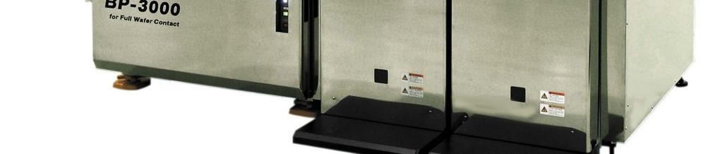
33 Micronics Japan Co. 34

34 Future Test Cell? 35
35 Summary Some challenges are 1.5x others are 2.25x Multiple solutions to technical challenges for R&D, short term, and long term Need to plan accordingly Largest challenge is financial Need right solution for each problem with proper return on investment (ROI) Don t want to over invest or miss the boat Inflection point enables innovation 36


36 450 mm 300 mm Can Stock Photo Inc. / andrewro 37
37 Acknowledgments Accretech Applied Materials Cascade Microtech Centipede Systems FormFactor Micronics Japan Co. (MJC) Multitest SPEA Tokyo Electron 38
38 Thank You! Ira Feldman Visit my blog for my summary of SWTW 39
39 References Cramming more components onto integrated circuits, Gordon E. Moore, Electronics, Volume 38, Number 8, April 19, Planning for the 300mm Transition, Daniel Seligson, Intel Technology Journal Q Position Paper for 450mm Development, International Technology Roadmap for Semiconductors (ITRS) Starting Materials Sub TWG, June
Are You Really Going to Package That? Ira Feldman Debbora Ahlgren
 Are You Really Going to Package That? Ira Feldman Debbora Ahlgren Feldman Engineering Corp. Outline Situation Cost of Test New Paradigm Probe Card Cost Drivers Computational Evolution New Approaches Conclusion
International Technology Roadmap for Semiconductors. Dave Armstrong Advantest Ira Feldman Feldman Engineering Marc Loranger - FormFactor
 International Technology Roadmap for Semiconductors Dave Armstrong Advantest Ira Feldman Feldman Engineering Marc - FormFactor Who are we? Why a roadmap? What is the purpose? Example Trends How can you
International Technology Roadmap for Semiconductors. Dave Armstrong Advantest Ira Feldman Feldman Engineering Marc Loranger FormFactor
 International Technology Roadmap for Semiconductors Dave Armstrong Advantest Ira Feldman Feldman Engineering Marc Loranger FormFactor Who are we? Why a roadmap? What is the purpose? Example Trends How
Progress due to: Feature size reduction - 0.7X/3 years (Moore s Law). Increasing chip size - 16% per year. Creativity in implementing functions.
. Increasing chip size - 16% per year. Creativity in implementing functions.") Introduction - Chapter 1 Evolution of IC Fabrication 1960 and 1990 integrated t circuits. it Progress due to: Feature size reduction - 0.7X/3 years (Moore s Law). Increasing chip size - 16% per year. Creativity
Introduction - Chapter 1 Evolution of IC Fabrication 1960 and 1990 integrated t circuits. it Progress due to: Feature size reduction - 0.7X/3 years (Moore s Law). Increasing chip size - 16% per year. Creativity
Testing of Complex Digital Chips. Juri Schmidt Advanced Seminar
 Testing of Complex Digital Chips Juri Schmidt Advanced Seminar - 11.02.2013 Outline Motivation Why testing is necessary Background Chip manufacturing Yield Reasons for bad Chips Design for Testability
450mm silicon wafers specification challenges. Mike Goldstein Intel Corp.
 450mm silicon wafers specification challenges Mike Goldstein Intel Corp. Outline Background 450mm transition program 450mm silicon evolution Mechanical grade wafers (spec case study) Developmental (test)
San Diego, CA, June 11 to 14, 2006
 To Advance Wafer Test Technology To Serve and Inform the Wafer Test Professional To Boldly Go Where No Workshop Has Gone Before San Diego, CA, June 11 to 14, 2006 16th Annual SWTW Probe Year In Review
Intel's 65 nm Logic Technology Demonstrated on 0.57 µm 2 SRAM Cells
 Intel's 65 nm Logic Technology Demonstrated on 0.57 µm 2 SRAM Cells Mark Bohr Intel Senior Fellow Director of Process Architecture & Integration Intel 1 What are We Announcing? Intel has fabricated fully-functional
ISSCC 2003 / SESSION 1 / PLENARY / 1.1
 ISSCC 2003 / SESSION 1 / PLENARY / 1.1 1.1 No Exponential is Forever: But Forever Can Be Delayed! Gordon E. Moore Intel Corporation Over the last fifty years, the solid-state-circuits industry has grown
SWTW 2000, June Assessing Pad Damage and Bond Integrity for Fine Pitch Probing
 SWTW 2000, June 11-14 Assessing Pad Damage and Bond Integrity for Fine Pitch Probing Dean Gahagan, Pyramid Probe Division, Cascade Microtech & Lee Levine, Kulicke & Soffa Industries Challenges of die shrinks
Manufacturing Case Studies: Copy Exactly (CE!) and the two-year cycle at Intel
 and the two-year cycle at Intel") Manufacturing Case Studies: Copy Exactly (CE!) and the two-year cycle at Intel Paolo A. Gargini Director Technology Strategy Intel Fellow 1 Agenda 2-year cycle Copy Exactly Conclusions 2 I see no reason
Manufacturing Case Studies: Copy Exactly (CE!) and the two-year cycle at Intel Paolo A. Gargini Director Technology Strategy Intel Fellow 1 Agenda 2-year cycle Copy Exactly Conclusions 2 I see no reason
Chapter 1, Introduction
 Introduction to Semiconductor Manufacturing Technology Chapter 1, Introduction hxiao89@hotmail.com 1 Objective After taking this course, you will able to Use common semiconductor terminology Describe a
Trends and Challenges in VLSI Technology Scaling Towards 100nm
 Trends and Challenges in VLSI Technology Scaling Towards 100nm Stefan Rusu Intel Corporation stefan.rusu@intel.com September 2001 Stefan Rusu 9/2001 2001 Intel Corp. Page 1 Agenda VLSI Technology Trends
Multiple Four Sided, Fine Pitch, Small Pad Devices
 1 2000 SouthWest Test Workshop A Method for Probing... Multiple Four Sided, Fine Pitch, Small Pad Devices... using Cantilever Probes Presented by: Louis Molinari Director of Engineering (480) 333-1579
ISMI Industry Productivity Driver
 SEMATECH Symposium Japan September 15, 2010 Accelerating Manufacturing Productivity ISMI Industry Productivity Driver Scott Kramer VP Manufacturing Technology SEMATECH Copyright 2010 SEMATECH, Inc. SEMATECH,
Testing of Chips Used for Artificial Intelligence. PH Chen, Project Management KeyStone Alan Liao, Product Marketing FormFactor
 Testing of Chips Used for Artificial Intelligence PH Chen, Project Management KeyStone Alan Liao, Product Marketing FormFactor Agenda Artificial Intelligence Evolution and Market Space Why AI Today AI
Challenges and More Challenges SW Test Workshop June 9, 2004
 Innovating Test Technologies Challenges and More Challenges SW Test Workshop June 9, 2004 Cascade Microtech Pyramid Probe Division Ken Smith Dean Gahagan Challenges and More Challenges Probe card requirements
1 Digital EE141 Integrated Circuits 2nd Introduction
 Digital Integrated Circuits Introduction 1 What is this lecture about? Introduction to digital integrated circuits + low power circuits Issues in digital design The CMOS inverter Combinational logic structures
450mm and Moore s Law Advanced Packaging Challenges and the Impact of 3D
 450mm and Moore s Law Advanced Packaging Challenges and the Impact of 3D Doug Anberg VP, Technical Marketing Ultratech SOKUDO Lithography Breakfast Forum July 10, 2013 Agenda Next Generation Technology
Introduction. Digital Integrated Circuits A Design Perspective. Jan M. Rabaey Anantha Chandrakasan Borivoje Nikolic. July 30, 2002
 Digital Integrated Circuits A Design Perspective Jan M. Rabaey Anantha Chandrakasan Borivoje Nikolic Introduction July 30, 2002 1 What is this book all about? Introduction to digital integrated circuits.
The future of lithography and its impact on design
 The future of lithography and its impact on design Chris Mack www.lithoguru.com 1 Outline History Lessons Moore s Law Dennard Scaling Cost Trends Is Moore s Law Over? Litho scaling? The Design Gap The
Advanced Stepper Lithography Technology to Enable Flexible AMOLED Displays. Keith Best Roger McCleary Elvino M da Silveira 5/19/17
 Advanced Stepper Lithography Technology to Enable Flexible AMOLED Displays Keith Best Roger McCleary Elvino M da Silveira 5/19/17 Agenda About Rudolph JetStep G System overview and performance Display
W ith development risk fully borne by the equipment industry and a two-year delay in the main
 Page 1 of 5 Economic Challenges and Opportunities in the 300 mm Transition Iddo Hadar, Jaim Nulman, Kunio Achiwa, and Oded Turbahn, Applied Materials Inc. -- 10/1/1998 Semiconductor International W ith
The Infinity Probe for On-Wafer Device Characterization and Modeling to 110 GHz
 Q & A Innovating Test Technologies The Infinity Probe for On-Wafer Device Characterization and Modeling to 110 GHz Why is this announcement important? INFINITY-QA-1102 Data subject to change without notice
IEEE Semiconductor Wafer Test Workshop June 10 to 13, 2012 at Rancho Bernardo Inn, San Diego, CA
 IEEE Semiconductor Wafer Test Workshop June 10 to 13, 2012 at Rancho Bernardo Inn, San Diego, CA Submitted by Jerry Broz, Ph.D., General Chair of IEEE SW Test and IEEE Senior Member Ira Feldman, IEEE Member
Lithography in our Connected World
 Lithography in our Connected World SEMI Austin Spring Forum TOP PAN P R INTING CO., LTD MATER IAL SOLUTIONS DIVISION Toppan Printing Co., LTD A Broad-Based Global Printing Company Foundation: January 17,
Comparison of Drilling Rates and Tolerances of Laser-Drilled holes in Silicon Nitride and Polyimide Vertical Probe Cards
 Dr. Alan Ferguson Oxford Lasers Comparison of Drilling Rates and Tolerances of Laser-Drilled holes in Silicon Nitride and Polyimide Vertical Probe Cards June 8-11, 8 2008 San Diego, CA USA Overview Introduction
Intel Technology Journal
 Volume 06 Issue 02 Published, May 16, 2002 ISSN 1535766X Intel Technology Journal Semiconductor Technology and Manufacturing The Intel Lithography Roadmap A compiled version of all papers from this issue
WLP Probing Technology Opportunity and Challenge. Clark Liu
 WLP Probing Technology Opportunity and Challenge Founded Capital PTI Group Overview : May/15/97 : USD 246 Millions PTI HQ Total Assets : USD 2.2B Employees Major Services : 11,100 (Greatek included) :
EMERGING SUBSTRATE TECHNOLOGIES FOR PACKAGING
 EMERGING SUBSTRATE TECHNOLOGIES FOR PACKAGING Henry H. Utsunomiya Interconnection Technologies, Inc. Suwa City, Nagano Prefecture, Japan henryutsunomiya@mac.com ABSTRACT This presentation will outline
Adaptive Patterning. ISS 2019 January 8th
 Creating a system to balance natural variation ISS 2019 January 8th Tim Olson Founder & CTO Let s start with an industry perspective Historically, three distinct electronic industry silos Foundries SATS
Optical lithography is the technique for
 By Chris A. Mack Snapshot: The author describes optical lithography in the context of the semiconductor industry. Past trends are evaluated and used to predict future possibilities. The economics of the
A Perspective on Semiconductor Equipment. R. B. Herring March 4, 2004
 A Perspective on Semiconductor Equipment R. B. Herring March 4, 2004 Outline Semiconductor Industry Overview of circuit fabrication Semiconductor Equipment Industry Some equipment business strategies Product
It s Time for 300mm Prime
 It s Time for 300mm Prime Iddo Hadar Managing Director, 300mm Prime Program Office SEMI Strategic Business Conference Napa Valley, California Tuesday, April 24, 2007 Safe Harbor Statement This presentation
B. Flip-Chip Technology
 B. Flip-Chip Technology B1. Level 1. Introduction to Flip-Chip techniques B1.1 Why flip-chip? In the development of packaging of electronics the aim is to lower cost, increase the packaging density, improve
21 rue La Noue Bras de Fer Nantes - France Phone : +33 (0) w7-foldite :
 w7-foldite :") 21 rue La Noue Bras de Fer 44200 - Nantes - France Phone : +33 (0) 240 180 916 - email : info@systemplus.fr - w7-foldite : www.systemplus.fr February 2013 Version 1 Written by: Sylvain HALLEREAU DISCLAIMER
21 rue La Noue Bras de Fer 44200 - Nantes - France Phone : +33 (0) 240 180 916 - email : info@systemplus.fr - w7-foldite : www.systemplus.fr February 2013 Version 1 Written by: Sylvain HALLEREAU DISCLAIMER
5G: THE NEXT DISRUPTIVE TECHNOLOGY IN PRODUCTION TEST
 5G: THE NEXT DISRUPTIVE TECHNOLOGY IN PRODUCTION TEST Daniel Bock, Ph.D. Mike Bishop Jeff Damm Michael Engelhardt Michael Hemena Robert Murphy Balbir Singh Introduction The development of 5G / WiGig products
The SEMATECH Model: Potential Applications to PV
 Continually cited as the model for a successful industry/government consortium Accelerating the next technology revolution The SEMATECH Model: Potential Applications to PV Dr. Michael R. Polcari President
Market and technology trends in advanced packaging
 Close Market and technology trends in advanced packaging Executive OVERVIEW Recent advances in device miniaturization trends have placed stringent requirements for all aspects of product manufacturing.
Production Test of Process Control Monitors (PCMs) with Pyramid Probe Cards
 with Pyramid Probe Cards") Production Test of Process Control Monitors (PCMs) with Pyramid Probe Cards Ken Smith, Cascade Microtech Bill Knauer, Keithley Instruments Dr. Jerry Broz, Jason Aronoff, Texas Instruments Goal of Presentation
Production Test of Process Control Monitors (PCMs) with Pyramid Probe Cards Ken Smith, Cascade Microtech Bill Knauer, Keithley Instruments Dr. Jerry Broz, Jason Aronoff, Texas Instruments Goal of Presentation
Opto-Mechanical Equipment of KBTEM: Present Day and the Future
 KBTEM JSC, Minsk, Belarus Opto-Mechanical Equipment of KBTEM: Present Day and the Future Quality Management System Certificate ISO-9001 since 2001 SPIE Member since 2003 www.kb-omo.by Dr. S.Avakaw SEMI
Wafer-Edge Challenges
 Wafer-Edge Challenges SEMI STEP Wafer Edge Profile SEMICON/West 2006 Tetsuo Fukuda SEMI Japan (Fujitsu) Japan Advanced Wafer Geometry Task Force SEMI Japan Abstract Issues on edge profile are discussed
DOC. NO. FT02000-S E FULLY AUTOMATIC PROBER SPECIFICATIONS TOKYO SEIMITSU CO., LTD.
 DOC. NO. FT02000-S 0 0 1- E1 1 1-18 -9 7 FULLY AUTOMATIC PROBER SPECIFICATIONS TOKYO SEIMITSU CO., LTD. TOKYO, JAPAN Contents of this document may be subject to change without notice. No part of this document
Technology for the MEMS processing and testing environment. SUSS MicroTec AG Dr. Hans-Georg Kapitza
 Technology for the MEMS processing and testing environment SUSS MicroTec AG Dr. Hans-Georg Kapitza 1 SUSS MicroTec Industrial Group Founded 1949 as Karl Süss KG GmbH&Co. in Garching/ Munich San Jose Waterbury
Photolithography I ( Part 1 )
") 1 Photolithography I ( Part 1 ) Chapter 13 : Semiconductor Manufacturing Technology by M. Quirk & J. Serda Bjørn-Ove Fimland, Department of Electronics and Telecommunication, Norwegian University of Science
1 Photolithography I ( Part 1 ) Chapter 13 : Semiconductor Manufacturing Technology by M. Quirk & J. Serda Bjørn-Ove Fimland, Department of Electronics and Telecommunication, Norwegian University of Science
HOW TO CONTINUE COST SCALING. Hans Lebon
 HOW TO CONTINUE COST SCALING Hans Lebon OUTLINE Scaling & Scaling Challenges Imec Technology Roadmap Wafer size scaling : 450 mm 2 COST SCALING IMPROVED PERFORMANCE 3 GLOBAL TRAFFIC FORECAST Cloud Traffic
Advanced Packaging Lithography and Inspection Solutions for Next Generation FOWLP-FOPLP Processing
 Advanced Packaging Lithography and Inspection Solutions for Next Generation FOWLP-FOPLP Processing Keith Best, Gurvinder Singh, and Roger McCleary Rudolph Technologies, Inc. 16 Jonspin Rd. Wilmington,
Practical Information
 EE241 - Spring 2010 Advanced Digital Integrated Circuits TuTh 3:30-5pm 293 Cory Practical Information Instructor: Borivoje Nikolić 550B Cory Hall, 3-9297, bora@eecs Office hours: M 10:30am-12pm Reader:
Multiple Patterning for Immersion Extension and EUV Insertion. Chris Bencher Distinguished Member of Technical Staff Applied Materials CTO group
 Multiple Patterning for Immersion Extension and EUV Insertion Chris Bencher Distinguished Member of Technical Staff Applied Materials CTO group Abstract Multiple Patterning for Immersion Extension and
Copyright 2003 by the Society of Photo-Optical Instrumentation Engineers.
 Copyright 2003 by the Society of Photo-Optical Instrumentation Engineers. This paper was published in the proceedings of Optical Microlithography XVI, SPIE Vol. 5040, pp. xxi-xxxi. It is made available
2008 IEEE Semiconductor Wafer Test Workshop
 2008 IEEE Semiconductor Wafer Test Workshop 18 th Annual SWTW You Are Here! Paradise Point and Spa, San Diego, CA Bill Mann (Chair Emeritus) Jerry Broz, Ph.D. (General Chair) Probe Year In Review With
ASML Market dynamics. Dave Chavoustie EVP Sales Analyst Day, September 30, 2004
 ASML Market dynamics Dave Chavoustie EVP Sales Analyst Day, September 30, 2004 Agenda! Market Overview! Growth Opportunities! 300mm Market! Asia Overview / Slide 2 ASML Unit Market Share Trend 60% 12 &
EMT 251 Introduction to IC Design
 EMT 251 Introduction to IC Design (Pengantar Rekabentuk Litar Terkamir) Semester II 2011/2012 Introduction to IC design and Transistor Fundamental Some Keywords! Very-large-scale-integration (VLSI) is
Economic Model Workshop, Philadelphia
 Economic Model Workshop, Philadelphia Denis Fandel, Project Manager, MM&P 1 August 2001 Meeting Guidelines Project Mission / Model Overview Early Production Test Program Fundamental Assumption Allocation
Welcome to the 24th Annual IEEE SW Test Workshop Jerry Broz, Ph.D.
 Welcome to the 24th Annual IEEE SW Test Workshop Jerry Broz, Ph.D. SW Test General Chair Twenty Four Years of Probe Technology Many thanks to all of the 7500+ attendees from around the world! J. Broz 2
CMP: Where have we been and where are we headed next? Robert L. Rhoades, Ph.D. NCCAVS CMPUG Meeting at Semicon West San Francisco, July 10, 2013
 CMP: Where have we been and where are we headed next? Robert L. Rhoades, Ph.D. NCCAVS CMPUG Meeting at Semicon West San Francisco, July 10, 2013 Outline Where have we been? Semiconductor Industry Birth
Enabling High Parallelism in Production RF Test
 Enabling High Parallelism in Production RF Test Patrick Rhodes Ryan Garrison Ram Lakshmanan FormFactor Connectivity is Driving Change The connected world is driving the growth of RFICs in the market. These
+1 (479)
") Introduction to VLSI Design http://csce.uark.edu +1 (479) 575-6043 yrpeng@uark.edu Invention of the Transistor Vacuum tubes ruled in first half of 20th century Large, expensive, power-hungry, unreliable
Introduction to VLSI Design http://csce.uark.edu +1 (479) 575-6043 yrpeng@uark.edu Invention of the Transistor Vacuum tubes ruled in first half of 20th century Large, expensive, power-hungry, unreliable
Disruptive Developments for Advanced Die Attach to Tackle the Challenges of Heterogeneous Integration
 Disruptive Developments for Advanced Die Attach to Tackle the Challenges of Heterogeneous Integration Hugo Pristauz & Andreas Mayr, Besi Austria presented by: Stefan Behler, Besi Switzerland ECTC 2018
NO COST APPLICATIONS FOR ASSEMBLY CYCLE TIME REDUCTION
 NO COST APPLICATIONS FOR ASSEMBLY CYCLE TIME REDUCTION Steven Brown, Joerg Domaschke, and Franz Leibl Siemens AG, HL MS Balanstrasse 73 Munich 81541, Germany email: steven.brown@siemens-scg.com KEY WORDS
3D-MEMS Probe for Fine Pitch Probing
 3D-MEMS Probe for Fine Pitch Probing Ryuichiro Mori R&D Japan Electronic Materials Corp. 2007 IEEE SW Test Workshop 1 Presentation Overview 1. Introduction JEM product overview 2. Objectives Challenges
Energy beam processing and the drive for ultra precision manufacturing
 Energy beam processing and the drive for ultra precision manufacturing An Exploration of Future Manufacturing Technologies in Response to the Increasing Demands and Complexity of Next Generation Smart
Test Structures Basics Part 1
 Test Structures Basics Part 1 By Christopher Henderson In this document we will provide an overview of test structures as they pertain to reliability. Test structures can provide critical insight into
4082A Parametric Test System Keysight 4080 Series
 4082A Parametric Test System Keysight 4080 Series Leading-edge technologies demand high performance semiconductor devices available at the lower cost-of-test in high volume manufacturing. Keysight offers
Core Business: Semiconductor-related Inspection Equipment
 Core Business: Semiconductor-related Inspection Equipment Lasertec manufactures unique inspection and measurement systems that incorporate the cutting-edge technologies of applied optics and offers them
International SEMATECH Wafer Probe Benchmarking Project WAFER PROBE ROADMAP. Guidance For Wafer Probe R&D Resources Edition
 International SEMATECH Wafer Probe Benchmarking Project WAFER PROBE ROADMAP Guidance For Wafer Probe R&D Resources 2002 Edition Fred Taber, IBM Microelectronics Probe Project Chair Gavin Gibson, Infineon
End-of-line Standard Substrates For the Characterization of organic
 FRAUNHOFER INSTITUTe FoR Photonic Microsystems IPMS End-of-line Standard Substrates For the Characterization of organic semiconductor Materials Over the last few years, organic electronics have become
Noel Technologies. Provider of Advanced Lithography and Semiconductor Thin Film Services
 Noel Technologies Provider of Advanced Lithography and Semiconductor Thin Film Services Noel Technologies Keith Best Biography Over the last 27 years, Keith Best has held a variety of semiconductor processing
A Presentation to the National Academies July 29, Larry W. Sumney President/CEO Semiconductor Research Corporation1
 A Presentation to the National Academies July 29, 2009 Larry W. Sumney President/CEO Semiconductor Research Corporation1 What is SRC? World s leading consortium funding collaborative university research
PAPER. Reducing parametric test costs with faster, smarter parallel test techniques
 WHITE PAPER Reducing parametric test costs with faster, smarter parallel test techniques Jeff Kuo, Steven Weinzierl, Keithley Instruments Glenn Alers, Gregory Harm, Novellus Systems Introduction The 1999
Can Nano-Coatings Really Improve Stencil Performance? Tony Lentz FCT Assembly
 Can Nano-Coatings Really Improve Stencil Performance? Tony Lentz FCT Assembly tlentz@fctassembly.com Outline/Agenda Introduction Claims & questions about coatings Experiment design Results of coating performance
Visible Light Photon R&D in the US. A. Bross KEK ISS Meeting January 25, 2006
 Visible Light Photon R&D in the US A. Bross KEK ISS Meeting January 25, 2006 Some History First VLPC History In 1987, a paper was published by Rockwell detailing the performance of Solid State PhotoMultipliers
Jan M. Rabaey Anantha Chandrakasan Borivoje Nikolic. July 30, Digital EE141 Integrated Circuits 2nd Introduction
 Digital Integrated Circuits A Design Perspective Jan M. Rabaey Anantha Chandrakasan Borivoje Nikolic Introduction July 30, 2002 1 What is this book all about? Introduction to digital integrated circuits.
POSSUM TM Die Design as a Low Cost 3D Packaging Alternative
 POSSUM TM Die Design as a Low Cost 3D Packaging Alternative The trend toward 3D system integration in a small form factor has accelerated even more with the introduction of smartphones and tablets. Integration
Public. Introduction to ASML. Ron Kool. SVP Corporate Strategy and Marketing. March-2015 Veldhoven
 Public Introduction to ASML Ron Kool SVP Corporate Strategy and Marketing March-2015 Veldhoven 1991 1992 1993 1994 1995 1996 1997 1998 1999 2000 2001 2002 2003 2004 2005 2006 2007 2008 2009 2010 2011 2012
Progress Towards Computer-Aided Design For Complex Photonic Integrated Circuits
 Department of Electrical and Computer Engineering Progress Towards Computer-Aided Design For Complex Photonic Integrated Circuits Wei-Ping Huang Department of Electrical and Computer Engineering McMaster
FPGA Based System Design
 FPGA Based System Design Reference Wayne Wolf, FPGA-Based System Design Pearson Education, 2004 Why VLSI? Integration improves the design: higher speed; lower power; physically smaller. Integration reduces
2 Integrated Circuit Manufacturing:
 2 Integrated Circuit Manufacturing: A Technology Resource 2 IC MANUFACTURING TECHNOLOGIES While the integrated circuit drives the packaging and assembly, the IC manufacturing process, and associated methodologies,
LSI ON GLASS SUBSTRATES
 LSI ON GLASS SUBSTRATES OUTLINE Introduction: Why System on Glass? MOSFET Technology Low-Temperature Poly-Si TFT Technology System-on-Glass Technology Issues Conclusion System on Glass CPU SRAM DRAM EEPROM
Flexline - A Flexible Manufacturing Method for Wafer Level Packages (Extended Abstract)
") Flexline - A Flexible Manufacturing Method for Wafer Level Packages (Extended Abstract) by Tom Strothmann, *Damien Pricolo, **Seung Wook Yoon, **Yaojian Lin STATS ChipPAC Inc.1711 W Greentree Drive Tempe,
Flexline - A Flexible Manufacturing Method for Wafer Level Packages (Extended Abstract) by Tom Strothmann, *Damien Pricolo, **Seung Wook Yoon, **Yaojian Lin STATS ChipPAC Inc.1711 W Greentree Drive Tempe,
DUV. Matthew McLaren Vice President Program Management, DUV. 24 November 2014
 DUV Matthew McLaren Vice President Program Management, DUV 24 Forward looking statements This document contains statements relating to certain projections and business trends that are forward-looking,
Announcements. Advanced Digital Integrated Circuits. Project proposals due today. Homework 1. Lecture 8: Gate delays,
 EE4 - Spring 008 Advanced Digital Integrated Circuits Lecture 8: Gate delays, Variability Announcements Project proposals due today Title Team members ½ page ~5 references Post it on your EECS web page
Improved ON-resistance Measurement at Wafer Probe using a "DARUMA" stage
 Improved ON-resistance Measurement at Wafer Probe using a "DARUMA" stage Masatomo TAKAHASHI ACCRETECH, Japan Nobuyuki TOYODA TESEC, Japan Background Trend of MOSFET Overview Solution DARUMA Transition
Fiber Optics for Harsh Environments ICSO Chuck Tabbert
 Fiber Optics for Harsh Environments ICSO 2016 Chuck Tabbert VP Sales & Marketing Ultra Communications (505) 823-1293 ctabbert@ultracomm-inc.com www.ultracomm-inc.com If anyone would like copy of briefing
Correlation of Wafer Backside Defects to Photolithography Hot Spots Using Advanced Macro Inspection
 Correlation of Wafer Defects to Photolithography Hot Spots Using Advanced Macro Inspection Alan Carlson* a, Tuan Le* a a Rudolph Technologies, 4900 West 78th Street, Bloomington, MN, USA 55435; Presented
Introduction to VLSI ASIC Design and Technology
 Introduction to VLSI ASIC Design and Technology Paulo Moreira CERN - Geneva, Switzerland Paulo Moreira Introduction 1 Outline Introduction Is there a limit? Transistors CMOS building blocks Parasitics
Used Semiconductor Manufacturing Equipment: Looking for Sales in All the Right Places. Study Number MA108-09
 Study Number MA108-09 August 2009 Copyright Semico Research, 2009. All rights reserved. Reproduction in whole or part is prohibited without permission of Semico. The contents of this report represent
Silicon Photonics Reliability and Qualification Testing
 Silicon Photonics Reliability and Qualification Testing Angelo Miele Manager Photonics Reliability, Lightwave BU Macom Technology Solutions Angelo.miele@macom.com Agenda 1. Silicon Photonics Design and
Lithography. Taking Sides to Optimize Wafer Surface Uniformity. Backside Inspection Applications In Lithography
 Lithography D E F E C T I N S P E C T I O N Taking Sides to Optimize Wafer Surface Uniformity Backside Inspection Applications In Lithography Kay Lederer, Matthias Scholze, Ulrich Strohbach, Infineon Technologies
Semiconductor Back-Grinding
 Semiconductor Back-Grinding The silicon wafer on which the active elements are created is a thin circular disc, typically 150mm or 200mm in diameter. During diffusion and similar processes, the wafer may
FinFET vs. FD-SOI Key Advantages & Disadvantages
 FinFET vs. FD-SOI Key Advantages & Disadvantages Amiad Conley Technical Marketing Manager Process Diagnostics & Control, Applied Materials ChipEx-2014, Apr 2014 1 Moore s Law The number of transistors
Photolithography Technology and Application
 Photolithography Technology and Application Jeff Tsai Director, Graduate Institute of Electro-Optical Engineering Tatung University Art or Science? Lind width = 100 to 5 micron meter!! Resolution = ~ 3
Competitive in Mainstream Products
 Competitive in Mainstream Products Bert Koek VP, Business Unit manager 300mm Fabs Analyst Day 20 September 2005 ASML Competitive in mainstream products Introduction Market share Device layers critical
Silicon VLSI Technology. Fundamentals, Practice and Modeling. Class Notes For Instructors. J. D. Plummer, M. D. Deal and P. B.
 Silicon VLSI Technology Fundamentals, ractice, and Modeling Class otes For Instructors J. D. lummer, M. D. Deal and. B. Griffin These notes are intended to be used for lectures based on the above text.
Scaling of Semiconductor Integrated Circuits and EUV Lithography
 Scaling of Semiconductor Integrated Circuits and EUV Lithography ( 半導体集積回路の微細化と EUV リソグラフィー ) December 13, 2016 EIDEC (Emerging nano process Infrastructure Development Center, Inc.) Hidemi Ishiuchi 1 OUTLINE
EE 330 Lecture 11. Capacitances in Interconnects Back-end Processing
 EE 330 Lecture 11 Capacitances in Interconnects Back-end Processing Exam 1 Friday Sept 21 Students may bring 1 page of notes HW assignment for week of Sept 16 due on Wed Sept 19 at beginning of class No
VLSI: An Introduction
 Chapter 1 UEEA2223/UEEG4223 Integrated Circuit Design VLSI: An Introduction Prepared by Dr. Lim Soo King 02 Jan 2011. Chapter 1 VLSI Design: An Introduction... 1 1.0 Introduction... 1 1.0.1 Early Computing
The end of Moore s law and the race for performance
 The end of Moore s law and the race for performance Michael Resch (HLRS) September 15, 2016, Basel, Switzerland Roadmap Motivation (HPC@HLRS) Moore s law Options Outlook HPC@HLRS Cray XC40 Hazelhen 185.376
Practical Information
 EE241 - Spring 2013 Advanced Digital Integrated Circuits MW 2-3:30pm 540A/B Cory Practical Information Instructor: Borivoje Nikolić 509 Cory Hall, 3-9297, bora@eecs Office hours: M 11-12, W 3:30pm-4:30pm
In 1951 William Shockley developed the world first junction transistor. One year later Geoffrey W. A. Dummer published the concept of the integrated
 Objectives History and road map of integrated circuits Application specific integrated circuits Design flow and tasks Electric design automation tools ASIC project MSDAP In 1951 William Shockley developed