Adaptive Patterning. ISS 2019 January 8th
|
|
|
- Gervase Palmer
- 5 years ago
- Views:
Transcription
1 Creating a system to balance natural variation ISS 2019 January 8th Tim Olson Founder & CTO

2 Let s start with an industry perspective Historically, three distinct electronic industry silos Foundries SATS EMS Semiconductor Devices Nanometers Packaging 10 s of Microns Electronic Systems 100 s of Microns
3 in past few years Blurring of lines to convergence Foundries SATS EMS


4 in past few years Blurring of lines to convergence Foundries SATS EMS With industry leaders investing across historic boundaries


5 Examples from industry leaders #1 Foundry #1 SATS #1 EMS TSMC Grew a new $2.5B business in wafer bumping, test, CoWoS & InFO ASE Grew a $1.4B wafer level and a $1.5B systems modules business Foxconn Launching $9B USD new chip fab through Sharp acquisition
 High Level Fan-out Process Chip First Fan Out Chips First Fan-out Wafer")

6 What technology s leading the convergence? Wafer Level Fan-out Technology (WLFO) High Level Fan-out Process Chip First Fan Out Chips First Fan-out Wafer Silicon Dicing Device Wafer Singulated Wafer Devices Chip Reconstitution Attached on Carrier Molded Molding Plastic Wafer RDL Formation Wafer Fab Processing Backend Processing Part assembly - SATS Part wafer fabrication - Foundry Part electronic system integration - EMS Flow courtesy of John Hunt, ASE


7 Fan-out - Let s take a look inside The concept The realization Backside Epoxy Silicon Device Cu Stud Mold Compound Planar Surface Cu RDL 1 3 layers Embedded Chip Note: Multiple patents granted & pending


8 M-Series Fan-out Process Modules

9 M-Series Basic Process Flow Die attach leads to # challenge in fan-out Die Shift
10 Die shift - #1 challenge in fan-out Precision of monolithic silicon is lost - semiconductor devices are singulated & recombined in a physically different format to re-create a 300mm wafer (in plastic) Two major sources of positional variation Die placement tolerance Die shift during molding Nominal designed positions Resulting chip position in fan-out wafer (panel) Nominal designed positions Actual measured positions
 post")
11 M-Series Basic Process Flow 300mm plastic wafer (panel) post planarization
12 M-Series Basic Process Flow Actual measurement data of 2,478 devices in a 300mm panel

13 Tax revenue How to solve the die shift challenge? Conventional linear thinking is usually the starting point i.e., Drive all sources of variation to zero to eliminate die shift Let s draw a corollary to something that impacts everyone in the room Taxes & Tariffs January 7, % 100% Tax rate Rep. Alexandria Ocasio-Cortez, D--N.Y. Proposing 70% tax rate! Conventional linear thinking Increase taxes & tariffs lead to increased tax revenue

14 Conventional linear thinking is the wrong model Taxes, Tariffs & the Laffer Curve Art Laffer economist, author, educator Source: Forbes 2012 Overcoming the classic failure of conventional linear thinking! 1974 Art Laffer met with Dick Cheney & Donald Rumsfeld drew his curve on a napkin
15 Back to solving the die shift challenge? Conventional linear thinking Use a high precision die attach machine Partially effective and very expensive


16 Just how expensive is it? Breakdown of capex for overall fan-out flow Pareto of top five capex items


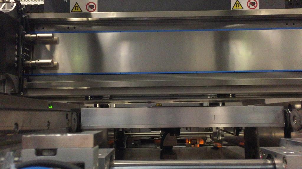
17 Deca 10X thinking the inspiration Space Invaders Use video gaming methodology to create real-time EDA in manufacturing.. adapting a nominal design to perfectly match the variation of every chip on every wafer We call it


18 Let s look at in action Deca s M-Series structure Deca test chip


19 in action Adaptive Alignment* Align the entire Cu interconnect pattern to the measured die position Adaptive Routing* Dynamically adapt Cu interconnect to the measured die position Enables high metal density designs Precisely aligns inductors to the die BGA array fixed to package outline Enables multi-die fan-out & SiP *Note: Multiple patents issued & pending
20 Adaptive Routing in Action A Fully Molded Fan-out Wafer Level Package
21 Multi-mode IoT Module 2 chips High performance MCU 40nm Bluetooth radio 55nm Package 5.0 x 3.8 mm 104 IO, 0.4mm pitch Die 1: 3.7 x 3.2 mm Die 2: 1.0 x 2.0 mm
22 Multi-mode


23 Multi-mode


24 Scale of Adaptive Patterning LSST - Large Synoptic Survey Telescope World s largest camera, 8.4m primary mirror Coming online in 2022 in Chile Maps the entire sky every two nights Deca s Adaptive Patterning 1 st real-time design in manufacturing In production since mm round reticle in single GDS II file LSST Camera Specs: 3.2 Gigapixels every 20 seconds 160 Megapixels per second Adaptive Patterning Specs: 300mm designed & exposed each 28 seconds 90 Gigapixel file, 3.2 Gigapixels per second 600mm next gen 2µm system 36 Terapixels in 140 seconds 257 Gigapixels per second

25 Back to our fan-out problem Die location measurement results why bimodal?

26 High speed die attach with dual gantries 20 nozzles per head, two heads = 28,000 cph
27

28 Adaptive Patterning Delivering > 10X capex cost breakthrough for die attach
29 Adaptive Patterning Conventional linear thinking Power of thinking differently Pareto of top five capex items Pareto of top five capex items


30 M-Series Building Blocks Direct Connect Thick Cu Low contact resistance, multi-via capture Polymer Isolated Via Further stress isolation, tighter design rules Multi-Layer, multi-thickness RDL & Dielectrics 10µm 5µm 2µm 5µm Nested Lines 5µm Isolated Line


31 Fan-out incorporating decades of learning Wafer fab bumping WLCSP Flip Chip Assembly Coreless Substrate Wafer Level MEMS Fan Out Fan Out Heterogeneous Integration Conformal Shielding Antenna on Package Fan Out Multidie Fan Out 3D 2.5D Interposer Graphic created by & courtesy of John Hunt, ASE
32 Why does it matter? Source: TechSearch International & Deca estimates


33 What s next? Integration of 4 reticle size chips in 80mm x 80mm format Graphics created by & courtesy of Craig Bishop, Mango Dynamics


34 What s next? Adaptive patterning with < 1µm total system inaccuracy Graphics created by & courtesy of Craig Bishop, Mango Dynamics


35 What s next? Scaling to 600mm wafers (panels) Future Production Initial production 300mm round Large panel format

36 What s next? Scaling to 600mm wafers (panels)

37 Why large panel M-Series? Wafer Processing Cost 300mm round baseline* 7% 5% 43% 45% Depreciation Materials *Estimated industry average COGS of M-Series with Adaptive Patterning Labor Fac, Ovhd, Other M-Series large panel fan-out has the potential for >30% cost reduction Capital productivity Material efficiency


")
38 Scaling to large panel in cooperation with ASE Initial Production Future Production 300mm round (post chip attach) (post mold & debond)

39 A Closing Thought What lies behind us and what lies before us are tiny matters compared to what lies within us. Ralph Waldo Emerson Ralph Waldo Emerson

40 Thank You
Fan-Out Solutions: Today, Tomorrow the Future Ron Huemoeller
 Fan-Out Solutions: Today, Tomorrow the Future Ron Huemoeller Corporate Vice President, WW RnD & Technology Strategy 1 In the Beginning ewlb 2 Fan Out Packaging Emerges Introduction of Fan Out (ewlb) Marketed
Flexline - A Flexible Manufacturing Method for Wafer Level Packages (Extended Abstract)
") Flexline - A Flexible Manufacturing Method for Wafer Level Packages (Extended Abstract) by Tom Strothmann, *Damien Pricolo, **Seung Wook Yoon, **Yaojian Lin STATS ChipPAC Inc.1711 W Greentree Drive Tempe,
Flexline - A Flexible Manufacturing Method for Wafer Level Packages (Extended Abstract) by Tom Strothmann, *Damien Pricolo, **Seung Wook Yoon, **Yaojian Lin STATS ChipPAC Inc.1711 W Greentree Drive Tempe,
The Future of Packaging ~ Advanced System Integration
 The Future of Packaging ~ Advanced System Integration Enabling a Microelectronic World R. Huemoeller SVP, Adv. Product / Platform Develop June 2013 Product Segments End Market % Share Summary 2 New Product
Disruptive Developments for Advanced Die Attach to Tackle the Challenges of Heterogeneous Integration
 Disruptive Developments for Advanced Die Attach to Tackle the Challenges of Heterogeneous Integration Hugo Pristauz & Andreas Mayr, Besi Austria presented by: Stefan Behler, Besi Switzerland ECTC 2018
Advanced Wafer Level Packaging of RF-MEMS with RDL Inductor
 Advanced Wafer Level Packaging of RF-MEMS with RDL Inductor Paul Castillou, Roberto Gaddi, Rob van Kampen, Yaojian Lin*, Babak Jamshidi** and Seung Wook Yoon*** Cavendish Kinetics, 2960 North First Street,
3D ICs: Recent Advances in the Industry
 3D ICs: Recent Advances in the Industry Suresh Ramalingam Senior Director, Advanced Packaging Outline 3D IC Background 3D IC Technology Development Summary Acknowledgements Stacked Silicon Interconnect
IMAPS NE 45 A HETEROGENEOUS SIP SOLUTION FOR RF APPLICATIONS
 IMAPS NE 45 A HETEROGENEOUS SIP SOLUTION FOR RF APPLICATIONS May 1st 2018 Justin C. Borski i3 Microsystems Inc. justin.borski@i3microsystems.com A HETEROGENEOUS SIP SOLUTION FOR RF APPLICATIONS Presentation
POSSUM TM Die Design as a Low Cost 3D Packaging Alternative
 POSSUM TM Die Design as a Low Cost 3D Packaging Alternative The trend toward 3D system integration in a small form factor has accelerated even more with the introduction of smartphones and tablets. Integration
Fan-Out Wafer Level Packaging Patent Landscape Analysis
 Fan-Out Wafer Level Packaging Patent Landscape Analysis Source: Infineon Source: TSMC Source: ASE November 2016 Source: Deca Technologies Source: STATS ChipPAC Source: Nepes KnowMade Patent & Technology
2D to 3d architectures: back to the future
 2D to 3d architectures: back to the future Raja Swaminathan Package architect Intel Corporation 2018 IMAPS Device Packaging Keynote, 03/06/2018 acknowledgements Ravi Mahajan, Ram Viswanath, Bob Sankman,
Expanding film and process for high efficiency 5 sides protection and FO-WLP fabrication
 2017 IEEE 67th Electronic Components and Technology Conference Expanding film and process for high efficiency 5 sides protection and FO-WLP fabrication Kazutaka Honda, Naoya Suzuki, Toshihisa Nonaka, Hirokazu
Fraunhofer IZM - ASSID
 FRAUNHOFER-INSTITUT FÜR Zuverlässigkeit und Mikrointegration IZM Fraunhofer IZM - ASSID All Silicon System Integration Dresden Heterogeneous 3D Wafer Level System Integration 3D system integration is one
Silicon Interposers enable high performance capacitors
 Interposers between ICs and package substrates that contain thin film capacitors have been used previously in order to improve circuit performance. However, with the interconnect inductance due to wire
Laminate Based Fan-Out Embedded Die Technologies: The Other Option
 Laminate Based Fan-Out Embedded Die Technologies: The Other Option Theodore (Ted) G. Tessier, Tanja Karila*, Tuomas Waris*, Mark Dhaenens and David Clark FlipChip International, LLC 3701 E University Drive
Semiconductor and LED Markets. Jon Sabol Vice President and General Manager Semiconductor and LED Division
 Semiconductor and LED Markets Jon Sabol Vice President and General Manager Semiconductor and LED Division Semiconductor & LED Investing in Semiconductor and LED $ Millions 300 200 27% CAGR 100 0 * FY06
450mm and Moore s Law Advanced Packaging Challenges and the Impact of 3D
 450mm and Moore s Law Advanced Packaging Challenges and the Impact of 3D Doug Anberg VP, Technical Marketing Ultratech SOKUDO Lithography Breakfast Forum July 10, 2013 Agenda Next Generation Technology
First Demonstration of Panel Glass Fan-out (GFO) Packages for High I/O Density and High Frequency Multi-Chip Integration
 Packages for High I/O Density and High Frequency Multi-Chip Integration") First Demonstration of Panel Glass Fan-out (GFO) Packages for High I/O Density and High Frequency Multi-Chip Integration Tailong Shi, Chintan Buch,Vanessa Smet, Yoichiro Sato, Lutz Parthier, Frank Wei
First Demonstration of Panel Glass Fan-out (GFO) Packages for High I/O Density and High Frequency Multi-Chip Integration Tailong Shi, Chintan Buch,Vanessa Smet, Yoichiro Sato, Lutz Parthier, Frank Wei
Packaging Roadmap: The impact of miniaturization. Bob Pfahl, inemi Celestica-iNEMI Technology Forum May 15, 2007
 Packaging Roadmap: The impact of miniaturization Bob Pfahl, inemi Celestica-iNEMI Technology Forum May 15, 2007 The Challenges for the Next Decade Addressing the consumer experience using the converged
EMERGING SUBSTRATE TECHNOLOGIES FOR PACKAGING
 EMERGING SUBSTRATE TECHNOLOGIES FOR PACKAGING Henry H. Utsunomiya Interconnection Technologies, Inc. Suwa City, Nagano Prefecture, Japan henryutsunomiya@mac.com ABSTRACT This presentation will outline
Diverse Lasers Support Key Microelectronic Packaging Tasks
 Diverse Lasers Support Key Microelectronic Packaging Tasks Written by D Muller, R Patzel, G Oulundsen, H Halou, E Rea 23 July 2018 To support more sophisticated and compact tablets, phones, watches and
Market and technology trends in advanced packaging
 Close Market and technology trends in advanced packaging Executive OVERVIEW Recent advances in device miniaturization trends have placed stringent requirements for all aspects of product manufacturing.
Min Tao, Ph. D, Ashok Prabhu, Akash Agrawal, Ilyas Mohammed, Ph. D, Bel Haba, Ph. D Oct , IWLPC
 PACKAGE-ON-PACKAGE INTERCONNECT FOR FAN-OUT WAFER LEVEL PACKAGES Min Tao, Ph. D, Ashok Prabhu, Akash Agrawal, Ilyas Mohammed, Ph. D, Bel Haba, Ph. D Oct 18-20 2016, IWLPC 1 Outline Laminate to Fan-Out
SiP packaging technology of intelligent sensor module. Tony li
 SiP packaging technology of intelligent sensor module Tony li 2016.9 Contents What we can do with sensors Sensor market trend Challenges of sensor packaging SiP technology to overcome challenges Overview
Advanced Packaging Lithography and Inspection Solutions for Next Generation FOWLP-FOPLP Processing
 Advanced Packaging Lithography and Inspection Solutions for Next Generation FOWLP-FOPLP Processing Keith Best, Gurvinder Singh, and Roger McCleary Rudolph Technologies, Inc. 16 Jonspin Rd. Wilmington,
Fan-Out Wafer Level Packaging Patent Landscape Analysis
 Fan-Out Wafer Level Packaging Patent Landscape Analysis Source: Infineon Source: TSMC Source: ASE November 2016 Source: Deca Technologies Source: STATS ChipPAC Source: Nepes KnowMade Patent & Technology
2.5D Platform (Examples of products produced to date are shown here to demonstrate Amkor's production capabilities)
") Wafer Finishing & Flip Chip Stacking interconnects have emerged to serve a wide range of 2.5D- & 3D- packaging applications and architectures that demand very high performance and functionality at the
Wafer Finishing & Flip Chip Stacking interconnects have emerged to serve a wide range of 2.5D- & 3D- packaging applications and architectures that demand very high performance and functionality at the
Manufacturing Development of a New Electroplated Magnetic Alloy Enabling Commercialization of PwrSoC Products
 Manufacturing Development of a New Electroplated Magnetic Alloy Enabling Commercialization of PwrSoC Products Trifon Liakopoulos, Amrit Panda, Matt Wilkowski and Ashraf Lotfi PowerSoC 2012 CONTENTS Definitions
Through Glass Via (TGV) Technology for RF Applications
 Technology for RF Applications") Through Glass Via (TGV) Technology for RF Applications C. H. Yun 1, S. Kuramochi 2, and A. B. Shorey 3 1 Qualcomm Technologies, Inc. 5775 Morehouse Dr., San Diego, California 92121, USA Ph: +1-858-651-5449,
Through Glass Via (TGV) Technology for RF Applications C. H. Yun 1, S. Kuramochi 2, and A. B. Shorey 3 1 Qualcomm Technologies, Inc. 5775 Morehouse Dr., San Diego, California 92121, USA Ph: +1-858-651-5449,
Electrical Test Vehicle for High Density Fan-Out WLP for Mobile Application. Institute of Microelectronics 22 April 2014
 Electrical Test Vehicle for High Density Fan-Out WLP for Mobile Application Institute of Microelectronics 22 April 2014 Challenges for HD Fan-Out Electrical Design 15-20 mm 7 mm 6 mm SI/PI with multilayer
Session 4: Mixed Signal RF
 Sophia Antipolis October 5 th & 6 th 2005 Session 4: Mixed Signal RF Technology, Design and Manufacture of RF SiP Chris Barratt, Michel Beghin, Insight SiP Insight SiP Summary Introduction Definition of
Yole Developpement. Developpement-v2585/ Publisher Sample
 Yole Developpement http://www.marketresearch.com/yole- Developpement-v2585/ Publisher Sample Phone: 800.298.5699 (US) or +1.240.747.3093 or +1.240.747.3093 (Int'l) Hours: Monday - Thursday: 5:30am - 6:30pm
New Wave SiP solution for Power
 New Wave SiP solution for Power Vincent Lin Corporate R&D ASE Group APEC March 7 th, 2018 in San Antonio, Texas. 0 Outline Challenges Facing Human Society Energy, Environment and Traffic Autonomous Driving
Design and Development of True-CSP
 Design and Development of True-CSP *Kolan Ravi Kanth, Francis K.S. Poh, B.K. Lim, Desmond Y.R. Chong, Anthony Sun, H.B. Tan United Test & Assembly Center Ltd (UTAC) 5 Serangoon North Ave 5, Singapore 554916
3D IC-Package-Board Co-analysis using 3D EM Simulation for Mobile Applications
 3D IC-Package-Board Co-analysis using 3D EM Simulation for Mobile Applications Darryl Kostka, CST of America Taigon Song and Sung Kyu Lim, Georgia Institute of Technology Outline Introduction TSV Array
Chapter 2. Literature Review
 Chapter 2 Literature Review 2.1 Development of Electronic Packaging Electronic Packaging is to assemble an integrated circuit device with specific function and to connect with other electronic devices.
Silicon Photonics Transceivers for Hyper Scale Datacenters: Deployment and Roadmap
 Silicon Photonics Transceivers for Hyper Scale Datacenters: Deployment and Roadmap Peter De Dobbelaere Luxtera Inc. 09/19/2016 Luxtera Proprietary www.luxtera.com Luxtera Company Introduction $100B+ Shift
Encapsulated Wafer Level Chip Scale Package (ewlcsp ) for Cost Effective and Robust Solutions in FlexLine
 for Cost Effective and Robust Solutions in FlexLine") Encapsulated Wafer Level Chip Scale Package (ewlcsp ) for Cost Effective and Robust Solutions in FlexLine by Yaojian Lin, Kang Chen, Kian Meng Heng, Linda Chua and *Seung Wook Yoon STATS ChipPAC Ltd. 5
Encapsulated Wafer Level Chip Scale Package (ewlcsp ) for Cost Effective and Robust Solutions in FlexLine by Yaojian Lin, Kang Chen, Kian Meng Heng, Linda Chua and *Seung Wook Yoon STATS ChipPAC Ltd. 5
Through-Silicon-Via Inductor: Is it Real or Just A Fantasy?
 Through-Silicon-Via Inductor: Is it Real or Just A Fantasy? Umamaheswara Rao Tida 1 Cheng Zhuo 2 Yiyu Shi 1 1 ECE Department, Missouri University of Science and Technology 2 Intel Research, Hillsboro Outline
CMP for Advanced Packaging
 CMP for Advanced Packaging Robert L. Rhoades, Ph.D. NCCAVS TFUG-CMPUG Joint Meeting June 9, 2016 Semiconductor Equipment Spare Parts and Service CMP Foundry Foundry Click to edit Master Outline title style
Foundry WLSI Technology for Power Management System Integration
 1 Foundry WLSI Technology for Power Management System Integration Chuei-Tang Wang, Chih-Lin Chen, Jeng-Shien Hsieh, Victor C.Y. Chang, Douglas Yu R&D,TSMC Oct. 2016 2 Motivation Outline PMIC system integration
Advanced Stepper Lithography Technology to Enable Flexible AMOLED Displays. Keith Best Roger McCleary Elvino M da Silveira 5/19/17
 Advanced Stepper Lithography Technology to Enable Flexible AMOLED Displays Keith Best Roger McCleary Elvino M da Silveira 5/19/17 Agenda About Rudolph JetStep G System overview and performance Display
TSV MEOL (Mid-End-Of-Line) and its Assembly/Packaging Technology for 3D/2.5D Solutions
 and its Assembly/Packaging Technology for 3D/2.5D Solutions") TSV MEOL (Mid-End-Of-Line) and its Assembly/Packaging Technology for 3D/2.5D Solutions Seung Wook YOON, D.J. Na, *K. T. Kang, W. K. Choi, C.B. Yong, *Y.C. Kim and Pandi C. Marimuthu STATS ChipPAC Ltd.
TSV MEOL (Mid-End-Of-Line) and its Assembly/Packaging Technology for 3D/2.5D Solutions Seung Wook YOON, D.J. Na, *K. T. Kang, W. K. Choi, C.B. Yong, *Y.C. Kim and Pandi C. Marimuthu STATS ChipPAC Ltd.
450mm patterning out of darkness Backend Process Exposure Tool SOKUDO Lithography Breakfast Forum July 10, 2013 Doug Shelton Canon USA Inc.
 450mm patterning out of darkness Backend Process Exposure Tool SOKUDO Lithography Breakfast Forum 2013 July 10, 2013 Doug Shelton Canon USA Inc. Introduction Half Pitch [nm] 2013 2014 2015 2016 2017 2018
B. Flip-Chip Technology
 B. Flip-Chip Technology B1. Level 1. Introduction to Flip-Chip techniques B1.1 Why flip-chip? In the development of packaging of electronics the aim is to lower cost, increase the packaging density, improve
Chapter 11 Testing, Assembly, and Packaging
 Chapter 11 Testing, Assembly, and Packaging Professor Paul K. Chu Testing The finished wafer is put on a holder and aligned for testing under a microscope Each chip on the wafer is inspected by a multiple-point
An Introduction to Electronics Systems Packaging. Prof. G. V. Mahesh. Department of Electronic Systems Engineering
 An Introduction to Electronics Systems Packaging Prof. G. V. Mahesh Department of Electronic Systems Engineering India Institute of Science, Bangalore Module No. # 02 Lecture No. # 08 Wafer Packaging Packaging
Beyond State-of-the-Art: Integration of MEMS in Fan-Out Wafer-Level Packaging Technology based System-in-Package (WLSiP)
") Beyond State-of-the-Art: Integration of MEMS in Fan-Out Wafer-Level Packaging Technology based System-in-Package (WLSiP) Steffen Kröhnert, Director of Technology André Cardoso, Senior R&D Integration Engineer
Beyond State-of-the-Art: Integration of MEMS in Fan-Out Wafer-Level Packaging Technology based System-in-Package (WLSiP) Steffen Kröhnert, Director of Technology André Cardoso, Senior R&D Integration Engineer
Innovations Push Package-on-Package Into New Markets. Flynn Carson. STATS ChipPAC Inc Kato Rd Fremont, CA 94538
 Innovations Push Package-on-Package Into New Markets by Flynn Carson STATS ChipPAC Inc. 47400 Kato Rd Fremont, CA 94538 Copyright 2010. Reprinted from Semiconductor International, April 2010. By choosing
Rudolph s JetStep Lithography System Maximizes Throughput while Addressing the Specific Challenges of Advanced Packaging Applications
 Rudolph s JetStep Lithography System Maximizes Throughput while Addressing the Specific Challenges of Advanced Packaging Applications Elvino da Silveira - Rudolph Technologies, Inc. ABSTRACT Rudolph s
Die Prep Considerations for IC Device Applications CORWIL Technology 1635 McCarthy Blvd Milpitas, CA 95035
 Die Prep Considerations for IC Device Applications CORWIL Technology 1635 McCarthy Blvd Milpitas, CA 95035 Jonny Corrao Die Prep While quality, functional parts are the end goal for all semiconductor companies,
Amkor s 2.5D Package and HDFO Advanced Heterogeneous Packaging Solutions
 Amkor s 2.5D Package and HDFO Advanced Heterogeneous Packaging Solutions John Lee, Sr. Director, Amkor Technology, Inc. Mike Kelly, VP, Adv Package & Technology Integration, Amkor Technology, Inc. Abstract:
Embedded Si Fan Out: A Low Cost Wafer Level Packaging Technology Without Molding and De-bonding Processes
 2017 IEEE 67th Electronic Components and Technology Conference Embedded Si Fan Out: A Low Cost Wafer Level Packaging Technology Without Molding and De-bonding Processes Daquan Yu*, Zhenrui Huang, Zhiyi
Enabling concepts: Packaging Technologies
 Enabling concepts: Packaging Technologies Ana Collado / Liam Murphy ESA / TEC-EDC 01/10/2018 ESA UNCLASSIFIED - For Official Use Enabling concepts: Packaging Technologies Drivers for the future: Higher
Oki 2BM6143 Microcontroller Unit Extracted from Casio GW2500 Watch 0.25 µm CMOS Process
 Oki 2BM6143 Microcontroller Unit Extracted from Casio GW2500 Watch 0.25 µm CMOS Process Custom Process Review with TEM Analysis For comments, questions, or more information about this report, or for any
The Design Challenge to Integrate High Performance Organic Packaging into High End ASIC Strategic Space Based Applications.
 The Design Challenge to Integrate High Performance Organic Packaging into High End ASIC Strategic Space Based Applications May 8, 2007 Abstract: The challenge to integrate high-end, build-up organic packaging
Considerations in High-Speed High Performance Die-Package-Board Co-Design. Jenny Jiang Altera Packaging Department October 2014
 Considerations in High-Speed High Performance Die-Package-Board Co-Design Jenny Jiang Altera Packaging Department October 2014 Why Co-Design? Complex Multi-Layer BGA Package Horizontal and vertical design
Integrated Photonics using the POET Optical InterposerTM Platform
 Integrated Photonics using the POET Optical InterposerTM Platform Dr. Suresh Venkatesan CIOE Conference Shenzhen, China Sept. 5, 2018 POET Technologies Inc. TSXV: PUBLIC POET PTK.V Technologies Inc. PUBLIC
TSI, or through-silicon insulation, is the
 Vertical through-wafer insulation: Enabling integration and innovation PETER HIMES, Silex Microsystems AB, Järfälla SWEDEN Through-wafer insulation has been used to develop technologies such as Sil-Via
Fabricating 2.5D, 3D, 5.5D Devices
 Fabricating 2.5D, 3D, 5.5D Devices Bob Patti, CTO rpatti@tezzaron.com Tezzar on Semiconduct or 04/15/2013 1 Gen4 Dis-Integrated 3D Memory DRAM layers 42nm node 2 million vertical connections per lay per
Application Bulletin 240
 Application Bulletin 240 Design Consideration CUSTOM CAPABILITIES Standard PC board fabrication flexibility allows for various component orientations, mounting features, and interconnect schemes. The starting
Advanced High-Density Interconnection Technology
 Advanced High-Density Interconnection Technology Osamu Nakao 1 This report introduces Fujikura s all-polyimide IVH (interstitial Via Hole)-multi-layer circuit boards and device-embedding technology. Employing
New Approaches to Develop a Scalable 3D IC Assembly Method
 New Approaches to Develop a Scalable 3D IC Assembly Method Charles G. Woychik Ph.D. Sangil Lee, Ph.D., Scott McGrath, Eric Tosaya and Sitaram Arkalgud Ph.D. Invensas Corporation 3025 Orchard Parkway San
Organic Packaging Substrate Workshop Overview
 Organic Packaging Substrate Workshop Overview Organized by: International Electronics Manufacturing Initiative (inemi) Mario A. Bolanos November 17-18, 2009 1 Organic Packaging Substrate Workshop Work
Technology Development & Integration Challenges for Lead Free Implementation. Vijay Wakharkar. Assembly Technology Development Intel Corporation
 Technology Development & Integration Challenges for Lead Free Implementation Vijay Wakharkar Assembly Technology Development Intel Corporation Legal Information THIS DOCUMENT AND RELATED MATERIALS AND
3D TSV Micro Cu Column Chip-to-Substrate/Chip Assmbly/Packaging Technology
 3D TSV Micro Cu Column Chip-to-Substrate/Chip Assmbly/Packaging Technology by Seung Wook Yoon, *K. T. Kang, W. K. Choi, * H. T. Lee, Andy C. B. Yong and Pandi C. Marimuthu STATS ChipPAC LTD, 5 Yishun Street
License to Speed: Extreme Bandwidth Packaging
 License to Speed: Extreme Bandwidth Packaging Sean S. Cahill VP, Technology BridgeWave Communications Santa Clara, California, USA BridgeWave Communications Specializing in 60-90 GHz Providing a wireless
Innovative Embedded Technologies to Enable Thinner IoT/Wearable/Mobile Devices
 Innovative Embedded Technologies to Enable Thinner IoT/Wearable/Mobile Devices Jensen Tsai Deputy Director, SPIL Building a Smarter World Wearable Internet of Things Building a Smarter World Mobile Devices
Lecture: Integration of silicon photonics with electronics. Prepared by Jean-Marc FEDELI CEA-LETI
 Lecture: Integration of silicon photonics with electronics Prepared by Jean-Marc FEDELI CEA-LETI Context The goal is to give optical functionalities to electronics integrated circuit (EIC) The objectives
CHAPTER 11: Testing, Assembly, and Packaging
 Chapter 11 1 CHAPTER 11: Testing, Assembly, and Packaging The previous chapters focus on the fabrication of devices in silicon or the frontend technology. Hundreds of chips can be built on a single wafer,
MICROELECTRONICS ASSSEMBLY TECHNOLOGIES. The QFN Platform as a Chip Packaging Foundation
 West Coast Luncheon January 15, 2014. PROMEX PROMEX INDUSTRIES INC. MICROELECTRONICS ASSSEMBLY TECHNOLOGIES The QFN Platform as a Chip Packaging Foundation 3075 Oakmead Village Drive Santa Clara CA Ɩ 95051
3D PLUS technology and offer
 3D PLUS technology and offer By Dr Pascal Couderc, 3D PLUS 408, Rue Hélène Boucher 78532 BUC France Phone: + 33 1 30 83 26 50 Email : www.3d-plus.com TM P.COUDERC 3D PLUS technology and offer 1 Outline
Recent Developments in Multifunctional Integration. Stephan Guttowski, Head of Technology Park»Heterointegration«, Fraunhofer FMD
 Recent Developments in Multifunctional Integration Stephan Guttowski, Head of Technology Park»Heterointegration«, Fraunhofer FMD Founding Participants 2 One-Stop-Shop for developments from wafer technologies
Ultra-thin Die Characterization for Stack-die Packaging
 Ultra-thin Die Characterization for Stack-die Packaging Wei Sun, W.H. Zhu, F.X. Che, C.K. Wang, Anthony Y.S. Sun and H.B. Tan United Test & Assembly Center Ltd (UTAC) Packaging Analysis & Design Center
Processes for Flexible Electronic Systems
 Processes for Flexible Electronic Systems Michael Feil Fraunhofer Institut feil@izm-m.fraunhofer.de Outline Introduction Single sheet versus reel-to-reel (R2R) Substrate materials R2R printing processes
!"#$"%&' ()#*+,-+.&/0(
#*+,-+.&/0(") !"#$"%&' ()#*+,-+.&/0( Multi Chip Modules (MCM) or Multi chip packaging Industry s first MCM from IBM. Generally MCMs are horizontal or two-dimensional modules. Defined as a single unit containing two
!"#$"%&' ()#*+,-+.&/0( Multi Chip Modules (MCM) or Multi chip packaging Industry s first MCM from IBM. Generally MCMs are horizontal or two-dimensional modules. Defined as a single unit containing two
Product Catalog. Semiconductor Intellectual Property & Technology Licensing Program
 Product Catalog Semiconductor Intellectual Property & Technology Licensing Program MANUFACTURING PROCESS TECHNOLOGY OVERVIEW 90 nm 130 nm 0.18 µm 0.25 µm 0.35 µm >0.40 µm Logic CMOS SOI CMOS SOI CMOS SOI
PANEL LEVEL PACKAGING A MANUFACTURING SOLUTION FOR COST-EFFECTIVE SYSTEMS
 PANEL LEVEL PACKAGING A MANUFACTURING SOLUTION FOR COST-EFFECTIVE SYSTEMS R. Aschenbrenner, K.-F. Becker, T. Braun, and A. Ostmann Fraunhofer Institute for Reliability and Microintegration Berlin, Germany
Intel Xeon E3-1230V2 CPU Ivy Bridge Tri-Gate 22 nm Process
 Intel Xeon E3-1230V2 CPU Structural Analysis 3685 Richmond Road, Suite 500, Ottawa, ON K2H 5B7 Canada Tel: 613-829-0414 www.chipworks.com Structural Analysis Some of the information in this report may
MID Manufacturing Process.
 3D Aerosol Jet Printing An Emerging MID Manufacturing Process. Dr. Martin Hedges Neotech Services MTP, Nuremberg, Germany info@neotechservices.com Aerosol Jet Printing Aerosol Jet Process Overview Current
Flip chip Assembly with Sub-micron 3D Re-alignment via Solder Surface Tension
 Flip chip Assembly with Sub-micron 3D Re-alignment via Solder Surface Tension Jae-Woong Nah*, Yves Martin, Swetha Kamlapurkar, Sebastian Engelmann, Robert L. Bruce, and Tymon Barwicz IBM T. J. Watson Research
Co-design for Low Warpage and High Reliability in Advanced Package with TSV- Free Interposer (TFI)
") 2017 IEEE 67th Electronic Components and Technology Conference Co-design for Low Warpage and High Reliability in Advanced Package with TSV- Free Interposer (TFI) F.X. Che*, M. Kawano, M.Z. Ding, Y. Han,
2017 IEEE 67th Electronic Components and Technology Conference Co-design for Low Warpage and High Reliability in Advanced Package with TSV- Free Interposer (TFI) F.X. Che*, M. Kawano, M.Z. Ding, Y. Han,
Thermal Management in the 3D-SiP World of the Future
 Thermal Management in the 3D-SiP World of the Future Presented by W. R. Bottoms March 181 th, 2013 Smaller, More Powerful Portable Devices Are Driving Up Power Density Power (both power delivery and power
Brief Introduction of Sigurd IC package Assembly
 Brief Introduction of Sigurd IC package Assembly Content Package Development Trend Product Brief Sawing type QFN Representative MEMS Product LGA Light Sensor Proximity Sensor High Yield Capability Low
TechSearch International, Inc. Corporate Overview E. Jan Vardaman, President
 TechSearch International, Inc. Corporate Overview E. Jan Vardaman, President Corporate Background Founded in 1987 and headquartered in Austin, Texas Recognized around the world as a leading consulting
EOTPR Customer Case Studies. EUFANET Workshop: Findings OPEN?
 EOTPR Customer Case Studies EUFANET Workshop: Findings OPEN? OUTLINE o EOTPR introduction basic scheme o EOTPR OPEN customer case studies o Open on BGA trace (evaluation) o Open on embedded BGA trace o
Two major features of this text
 Two major features of this text Since explanatory materials are systematically made based on subject examination questions, preparation
Flexible Hybrid Electronics Fabricated with High-Performance COTS ICs using RTI CircuitFilm TM Technology
 Flexible Hybrid Electronics Fabricated with High-Performance COTS ICs using RTI CircuitFilm TM Technology Scott Goodwin 1, Erik Vick 2 and Dorota Temple 2 1 Micross Advanced Interconnect Technology Micross
SHELLCASE-TYPE WAFER-LEVEL PACKAGING SOLUTIONS: RF CHARACTERIZATION AND MODELING
 SHELLCASE-TYPE WAFER-LEVEL PACKAGING SOLUTIONS: RF CHARACTERIZATION AND MODELING M Bartek 1, S M Sinaga 1, G Zilber 2, D Teomin 2, A Polyakov 1, J N Burghartz 1 1 Delft University of Technology, Lab of
Low Thermal Resistance Flip-Chip Bonding of 850nm 2-D VCSEL Arrays Capable of 10 Gbit/s/ch Operation
 Low Thermal Resistance Flip-Chip Bonding of 85nm -D VCSEL Arrays Capable of 1 Gbit/s/ch Operation Hendrik Roscher In 3, our well established technology of flip-chip mounted -D 85 nm backside-emitting VCSEL
Sharp NC Megapixel CCD Imager Process Review
 Sharp NC9360 2.0 Megapixel CCD Imager Process Review For comments, questions, or more information about this report, or for any additional technical needs concerning semiconductor technology, please call
Lithography in our Connected World
 Lithography in our Connected World SEMI Austin Spring Forum TOP PAN P R INTING CO., LTD MATER IAL SOLUTIONS DIVISION Toppan Printing Co., LTD A Broad-Based Global Printing Company Foundation: January 17,
MICROBUMP LITHOGRAPHY FOR 3D STACKING APPLICATIONS
 MICROBUMP LITHOGRAPHY FOR 3D STACKING APPLICATIONS Patrick Jaenen, John Slabbekoorn, Andy Miller IMEC Kapeldreef 75 B-3001 Leuven, Belgium millera@imec.be Warren W. Flack, Manish Ranjan, Gareth Kenyon,
9 rue Alfred Kastler - BP Nantes Cedex 3 - France Phone : +33 (0) website :
 website :") 9 rue Alfred Kastler - BP 10748-44307 Nantes Cedex 3 - France Phone : +33 (0) 240 180 916 - email : info@systemplus.fr - website : www.systemplus.fr April 2012 - Version 1 Written by: Romain FRAUX DISCLAIMER
9 rue Alfred Kastler - BP 10748-44307 Nantes Cedex 3 - France Phone : +33 (0) 240 180 916 - email : info@systemplus.fr - website : www.systemplus.fr April 2012 - Version 1 Written by: Romain FRAUX DISCLAIMER
Electronic Costing & Technology Experts
 Electronic Costing & Technology Experts 21 rue la Nouë Bras de Fer 44200 Nantes France Phone : +33 (0) 240 180 916 email : info@systemplus.fr www.systemplus.fr September 2016 Version 1 Written by Stéphane
Trends in Advanced Packaging Technologies An IMAPS UK view
 Trends in Advanced Packaging Technologies An IMAPS UK view Andy Longford Chair IMAPS UK 2007 9 PandA Europe IMAPS UK IeMRC Interconnection event December 2008 1 International Microelectronics And Packaging
Integration of 3D detector systems
 Integration of 3D detector systems Piet De Moor Introduction Evolution in radiation detection/imaging: single pixel linear array 2D array increase in resolution = decrease in pitch (down to few um) = thanks
Part 5-1: Lithography
 Part 5-1: Lithography Yao-Joe Yang 1 Pattern Transfer (Patterning) Types of lithography systems: Optical X-ray electron beam writer (non-traditional, no masks) Two-dimensional pattern transfer: limited
alpha Stencils Ultra-high precision stencils for semi conductor manufacturing ALPHA Flux WLCSP Flux deposition stencils
 alpha Stencils Alpha Ultra-high precision stencils for semi conductor manufacturing ALPHA Flux WLCSP Flux deposition stencils ALPHA Sphere WLCSP Ball placement stencils ALPHA Bump bumping solder paste
3D Integration Using Wafer-Level Packaging
 3D Integration Using Wafer-Level Packaging July 21, 2008 Patty Chang-Chien MMIC Array Receivers & Spectrographs Workshop Pasadena, CA Agenda Wafer-Level Packaging Technology Overview IRAD development on
The 3D Silicon Leader
 The 3D Silicon Leader 3D Silicon IPD for smaller and more reliable Implantable Medical Devices ATW on Advanced Packaging for Wireless Medical Devices Mohamed Mehdi Jatlaoui, Sébastien Leruez, Olivier Gaborieau,