3D PLUS technology and offer
|
|
|
- William Burns
- 5 years ago
- Views:
Transcription

1 3D PLUS technology and offer By Dr Pascal Couderc, 3D PLUS 408, Rue Hélène Boucher BUC France Phone: TM P.COUDERC 3D PLUS technology and offer 1
2 Outline - Introduction - 3D PLUS technology - Product examples - Conclusions P.COUDERC 3D PLUS technology and offer 2
3 Introduction - Spin off from Thales (1996) - Located in Buc (France ), South of Paris - From September 2011, 3D PLUS is a 100% subsidiary of HEICO company - Strong R&D from the 3D PLUS launching - Active patenting policy - Space certifications from CNES, ESA, NASA, JPL,JAXA, CAST etc ( more than modules in space including ROSETTA mission cameras ) - Exportation: 90% - Workforce : R&D : 11 including 5 PhD P.COUDERC 3D PLUS technology and offer 3

")


 2")


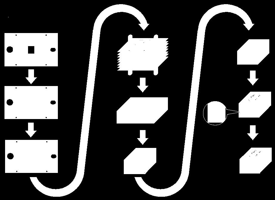

4 3D PLUS technology 1 ) - Flex Design 4 ) Layers Stacking 5 ) Cube Molding FLOW 2 process 7 ) Cube Plating ( Ni + Au ) 2 ) Components attachment 8 ) Circuit interconnection by laser grooving 3 ) - Circuit Test & Screening 6 ) Cube Sawing 9 ) Cube Test & Screening P.COUDERC 3D PLUS technology and offer 4
5 WDoD (1) initial criteria WDoD TM technology Use of multi sourcing wafers Stacking of 5 to 10 levels per mm Size: 200µm around the larger Die Stacking of Known Good Rebuilt Wafer (KGRW) Possibility of several dice of different dimensions of the same level Parallel processing/panelization from A to Z Possibility to stack PCB levels ( flow 2) and rebuilt wafers in order to optimize performances and costs (1) Wirefree Die on Die Trade Mark from 3D PLUS P.COUDERC 3D PLUS technology and offer 5
6 WDoD TM technology P.COUDERC 3D PLUS technology and offer 6

7 WDoD TM technology Dielectric passivation layer Metal track 2D routing: RDL Si Molding resin Al Pads P.COUDERC 3D PLUS technology and offer 7


8 WDoD TM technology 300 mm wafer Single unit 2 layers RDL with ground plane Via interconnect at Al pad level RDL cross section P.COUDERC 3D PLUS technology and offer 8

9 WDoD TM technology P.COUDERC 3D PLUS technology and offer 9


10 WDoD TM technology Laser patterning P.COUDERC 3D PLUS technology and offer 10


11 WDoD TM technology PoP and WDoD package relative sizes P.COUDERC 3D PLUS technology and offer 11
 The module has 5 layers stacked using 3D")
 and active components (3) and are")
 P.")
12 Product example 1 : Leadless pacemaker Dimensions : 2.3 x 5.2 x 7.3 mm (courtesy of SORIN CRM) The module has 5 layers stacked using 3D PLUS WDoD TM process. The layers are stacked at wafer level. 2 layers have known good passive (30) and active components (3) and are reconstituted wafers using fan out WLP technology ewlb. RDL pitch is 50µm. The 3 other layers are PCB based(mixed flow2 and WDoD) P.COUDERC 3D PLUS technology and offer 12


13 Bank2 Bank5 Bank4 Product Example 2 :Embedded programmable module Same footprint as a single SPARTAN 6 CSG484 The two dimensional area gain on a board is about 58 % Embedded decoupling capacitors 8Mx16 166MHz mddr 8Mx16 166MHz mddr 64Mb 104MHz NOR SPI Spartan 6 FPGA 6 CMT 4 GTPs JTAG Bank3 Bank1 Bank caps P.COUDERC 3D PLUS technology and offer 13


14 Product Example 2 : Embedded programmable module MODULE DIMENSIONS : 19 x19 x 3 mm BALLING : 484 SAC305 balls SAME BALL OUT THAN FPGA COMPONENT P.COUDERC 3D PLUS technology and offer 14
15 Conclusions-Offer With 3D PLUS technologies patented portfio, we can design, manufacture and performed electrical tests on 3D modules We have a large portfolio of standard 3D modules We can also develop and manufacture 3D modules for specific customers applications Our technologies are good alternatives to flex-folded, TSV, PoP, Chip-On-Chip technologies. P.COUDERC 3D PLUS technology and offer 15

16 Questions? Ultra Dense 3-D Micro system with WDoD Thank you for your attention P.COUDERC 3D PLUS technology and offer 16
Application of 3D PLUS WDoD technology for the manufacturing of electronic modules 25/02/2017 for implantable medical products
 Application of 3D PLUS WDoD TM technology for the manufacturing of electronic modules for implantable medical products By Dr Pascal Couderc 1, Karima Amara², Frederic Minault 2 3D PLUS 1 408, Rue Hélène
New wafer level stacking technologies and their applications
 New wafer level stacking technologies and their applications WDoD a new 3D PLUS technology Timothee Dargnies 3D PLUS USA Santa Clara, CA 1 Table of Contents Review of existing wafer level assembly processes
EUFANET. Full Wafer Level Stacking without TSV Applications to Memory-only and heterogeneous SiP
 EUFANET Full Wafer Level Stacking without TSV Applications to Memory-only and heterogeneous SiP Presented by Dr Christian Val Co-founder and CEO of 3D Plus 408 rue Hélène Boucher 78532 BUC (France) cval@3d-plus.com
Electronic Costing & Technology Experts
 Electronic Costing & Technology Experts 21 rue la Nouë Bras de Fer 44200 Nantes France Phone : +33 (0) 240 180 916 email : info@systemplus.fr www.systemplus.fr September 2016 Version 1 Written by Stéphane
Laminate Based Fan-Out Embedded Die Technologies: The Other Option
 Laminate Based Fan-Out Embedded Die Technologies: The Other Option Theodore (Ted) G. Tessier, Tanja Karila*, Tuomas Waris*, Mark Dhaenens and David Clark FlipChip International, LLC 3701 E University Drive
SiP packaging technology of intelligent sensor module. Tony li
 SiP packaging technology of intelligent sensor module Tony li 2016.9 Contents What we can do with sensors Sensor market trend Challenges of sensor packaging SiP technology to overcome challenges Overview
Min Tao, Ph. D, Ashok Prabhu, Akash Agrawal, Ilyas Mohammed, Ph. D, Bel Haba, Ph. D Oct , IWLPC
 PACKAGE-ON-PACKAGE INTERCONNECT FOR FAN-OUT WAFER LEVEL PACKAGES Min Tao, Ph. D, Ashok Prabhu, Akash Agrawal, Ilyas Mohammed, Ph. D, Bel Haba, Ph. D Oct 18-20 2016, IWLPC 1 Outline Laminate to Fan-Out
Fan-Out Solutions: Today, Tomorrow the Future Ron Huemoeller
 Fan-Out Solutions: Today, Tomorrow the Future Ron Huemoeller Corporate Vice President, WW RnD & Technology Strategy 1 In the Beginning ewlb 2 Fan Out Packaging Emerges Introduction of Fan Out (ewlb) Marketed
2D to 3d architectures: back to the future
 2D to 3d architectures: back to the future Raja Swaminathan Package architect Intel Corporation 2018 IMAPS Device Packaging Keynote, 03/06/2018 acknowledgements Ravi Mahajan, Ram Viswanath, Bob Sankman,
Fan-Out Wafer Level Packaging Patent Landscape Analysis
 Fan-Out Wafer Level Packaging Patent Landscape Analysis Source: Infineon Source: TSMC Source: ASE November 2016 Source: Deca Technologies Source: STATS ChipPAC Source: Nepes KnowMade Patent & Technology
Silicon Interposers enable high performance capacitors
 Interposers between ICs and package substrates that contain thin film capacitors have been used previously in order to improve circuit performance. However, with the interconnect inductance due to wire
Flexline - A Flexible Manufacturing Method for Wafer Level Packages (Extended Abstract)
") Flexline - A Flexible Manufacturing Method for Wafer Level Packages (Extended Abstract) by Tom Strothmann, *Damien Pricolo, **Seung Wook Yoon, **Yaojian Lin STATS ChipPAC Inc.1711 W Greentree Drive Tempe,
Flexline - A Flexible Manufacturing Method for Wafer Level Packages (Extended Abstract) by Tom Strothmann, *Damien Pricolo, **Seung Wook Yoon, **Yaojian Lin STATS ChipPAC Inc.1711 W Greentree Drive Tempe,
Advanced High-Density Interconnection Technology
 Advanced High-Density Interconnection Technology Osamu Nakao 1 This report introduces Fujikura s all-polyimide IVH (interstitial Via Hole)-multi-layer circuit boards and device-embedding technology. Employing
TSV MEOL (Mid-End-Of-Line) and its Assembly/Packaging Technology for 3D/2.5D Solutions
 and its Assembly/Packaging Technology for 3D/2.5D Solutions") TSV MEOL (Mid-End-Of-Line) and its Assembly/Packaging Technology for 3D/2.5D Solutions Seung Wook YOON, D.J. Na, *K. T. Kang, W. K. Choi, C.B. Yong, *Y.C. Kim and Pandi C. Marimuthu STATS ChipPAC Ltd.
TSV MEOL (Mid-End-Of-Line) and its Assembly/Packaging Technology for 3D/2.5D Solutions Seung Wook YOON, D.J. Na, *K. T. Kang, W. K. Choi, C.B. Yong, *Y.C. Kim and Pandi C. Marimuthu STATS ChipPAC Ltd.
SAMPLE REPACKAGING FOR BACKSIDE ANALYSIS
 SAMPLE REPACKAGING FOR BACKSIDE ANALYSIS CHAUDAT Willy, CNES /UPS CHAZAL Vanessa, Thales-CNES LAUVERJAT Dorine, Hirex Engineering FORGERIT Bertrand, Hirex Engineering 1 OUTLINE Context Process description
Fraunhofer IZM - ASSID
 FRAUNHOFER-INSTITUT FÜR Zuverlässigkeit und Mikrointegration IZM Fraunhofer IZM - ASSID All Silicon System Integration Dresden Heterogeneous 3D Wafer Level System Integration 3D system integration is one
Disruptive Developments for Advanced Die Attach to Tackle the Challenges of Heterogeneous Integration
 Disruptive Developments for Advanced Die Attach to Tackle the Challenges of Heterogeneous Integration Hugo Pristauz & Andreas Mayr, Besi Austria presented by: Stefan Behler, Besi Switzerland ECTC 2018
The 3D Silicon Leader
 The 3D Silicon Leader 3D Silicon IPD for smaller and more reliable Implantable Medical Devices ATW on Advanced Packaging for Wireless Medical Devices Mohamed Mehdi Jatlaoui, Sébastien Leruez, Olivier Gaborieau,
Enabling concepts: Packaging Technologies
 Enabling concepts: Packaging Technologies Ana Collado / Liam Murphy ESA / TEC-EDC 01/10/2018 ESA UNCLASSIFIED - For Official Use Enabling concepts: Packaging Technologies Drivers for the future: Higher
!"#$"%&' ()#*+,-+.&/0(
#*+,-+.&/0(") !"#$"%&' ()#*+,-+.&/0( Multi Chip Modules (MCM) or Multi chip packaging Industry s first MCM from IBM. Generally MCMs are horizontal or two-dimensional modules. Defined as a single unit containing two
!"#$"%&' ()#*+,-+.&/0( Multi Chip Modules (MCM) or Multi chip packaging Industry s first MCM from IBM. Generally MCMs are horizontal or two-dimensional modules. Defined as a single unit containing two
Flexible Hybrid Electronics Fabricated with High-Performance COTS ICs using RTI CircuitFilm TM Technology
 Flexible Hybrid Electronics Fabricated with High-Performance COTS ICs using RTI CircuitFilm TM Technology Scott Goodwin 1, Erik Vick 2 and Dorota Temple 2 1 Micross Advanced Interconnect Technology Micross
EMERGING SUBSTRATE TECHNOLOGIES FOR PACKAGING
 EMERGING SUBSTRATE TECHNOLOGIES FOR PACKAGING Henry H. Utsunomiya Interconnection Technologies, Inc. Suwa City, Nagano Prefecture, Japan henryutsunomiya@mac.com ABSTRACT This presentation will outline
Advanced Wafer Level Packaging of RF-MEMS with RDL Inductor
 Advanced Wafer Level Packaging of RF-MEMS with RDL Inductor Paul Castillou, Roberto Gaddi, Rob van Kampen, Yaojian Lin*, Babak Jamshidi** and Seung Wook Yoon*** Cavendish Kinetics, 2960 North First Street,
Chapter 11 Testing, Assembly, and Packaging
 Chapter 11 Testing, Assembly, and Packaging Professor Paul K. Chu Testing The finished wafer is put on a holder and aligned for testing under a microscope Each chip on the wafer is inspected by a multiple-point
9 rue Alfred Kastler - BP Nantes Cedex 3 - France Phone : +33 (0) website :
 website :") 9 rue Alfred Kastler - BP 10748-44307 Nantes Cedex 3 - France Phone : +33 (0) 240 180 916 - email : info@systemplus.fr - website : www.systemplus.fr April 2012 - Version 1 Written by: Romain FRAUX DISCLAIMER
9 rue Alfred Kastler - BP 10748-44307 Nantes Cedex 3 - France Phone : +33 (0) 240 180 916 - email : info@systemplus.fr - website : www.systemplus.fr April 2012 - Version 1 Written by: Romain FRAUX DISCLAIMER
Electroless Bumping for 300mm Wafers
 Electroless Bumping for 300mm Wafers T. Oppert Internepcon 2006 Tokyo Big Sight, Japan Outline Short Company Profile Electroless Ni/Au Under Bump Metallization UBM for Copper Devices Solder Bumping: Stencil
3D TSV Micro Cu Column Chip-to-Substrate/Chip Assmbly/Packaging Technology
 3D TSV Micro Cu Column Chip-to-Substrate/Chip Assmbly/Packaging Technology by Seung Wook Yoon, *K. T. Kang, W. K. Choi, * H. T. Lee, Andy C. B. Yong and Pandi C. Marimuthu STATS ChipPAC LTD, 5 Yishun Street
Innovations Push Package-on-Package Into New Markets. Flynn Carson. STATS ChipPAC Inc Kato Rd Fremont, CA 94538
 Innovations Push Package-on-Package Into New Markets by Flynn Carson STATS ChipPAC Inc. 47400 Kato Rd Fremont, CA 94538 Copyright 2010. Reprinted from Semiconductor International, April 2010. By choosing
New Wave SiP solution for Power
 New Wave SiP solution for Power Vincent Lin Corporate R&D ASE Group APEC March 7 th, 2018 in San Antonio, Texas. 0 Outline Challenges Facing Human Society Energy, Environment and Traffic Autonomous Driving
The Future of Packaging ~ Advanced System Integration
 The Future of Packaging ~ Advanced System Integration Enabling a Microelectronic World R. Huemoeller SVP, Adv. Product / Platform Develop June 2013 Product Segments End Market % Share Summary 2 New Product
MID Manufacturing Process.
 3D Aerosol Jet Printing An Emerging MID Manufacturing Process. Dr. Martin Hedges Neotech Services MTP, Nuremberg, Germany info@neotechservices.com Aerosol Jet Printing Aerosol Jet Process Overview Current
2.5D Platform (Examples of products produced to date are shown here to demonstrate Amkor's production capabilities)
") Wafer Finishing & Flip Chip Stacking interconnects have emerged to serve a wide range of 2.5D- & 3D- packaging applications and architectures that demand very high performance and functionality at the
Wafer Finishing & Flip Chip Stacking interconnects have emerged to serve a wide range of 2.5D- & 3D- packaging applications and architectures that demand very high performance and functionality at the
POSSUM TM Die Design as a Low Cost 3D Packaging Alternative
 POSSUM TM Die Design as a Low Cost 3D Packaging Alternative The trend toward 3D system integration in a small form factor has accelerated even more with the introduction of smartphones and tablets. Integration
Adaptive Patterning. ISS 2019 January 8th
 Creating a system to balance natural variation ISS 2019 January 8th Tim Olson Founder & CTO Let s start with an industry perspective Historically, three distinct electronic industry silos Foundries SATS
3D ICs: Recent Advances in the Industry
 3D ICs: Recent Advances in the Industry Suresh Ramalingam Senior Director, Advanced Packaging Outline 3D IC Background 3D IC Technology Development Summary Acknowledgements Stacked Silicon Interconnect
n o. 03 / O ct Newsletter
 www.hermes-ect.net n o. 03 / O ct. 2011 Newsletter Content Issue No. 3: Welcome to the third issue of the HERMES Newsletter! I. Progress of HERMES in Year 3 Progress of HERMES in Year 3 II. EDA tools for
AuthenTec AES1710 Secure Slide Fingerprint Sensor
 AuthenTec AES1710 Secure Slide Fingerprint Sensor Package Analysis For comments, questions, or more information about this report, or for any additional technical needs concerning semiconductor technology,
PCB technologies and manufacturing General Presentation
 PCB technologies and manufacturing General Presentation 1 Date : December 2014 3 plants for a global offer dedicated to the European market and export Special technologies, Harsh environment PCB for space
Enabling Parallel Testing at Sort for High Power Products
 Enabling Parallel Testing at Sort for High Power Products Abdel Abdelrahman Tim Swettlen 2200 Mission College Blvd. M/S SC2-07 Santa Clara, CA 94536 Abdel.Abdelrahman@intel.com Tim.Swettlen@intel.com Agenda
Semiconductor and LED Markets. Jon Sabol Vice President and General Manager Semiconductor and LED Division
 Semiconductor and LED Markets Jon Sabol Vice President and General Manager Semiconductor and LED Division Semiconductor & LED Investing in Semiconductor and LED $ Millions 300 200 27% CAGR 100 0 * FY06
Fan-Out Wafer Level Packaging Patent Landscape Analysis
 Fan-Out Wafer Level Packaging Patent Landscape Analysis Source: Infineon Source: TSMC Source: ASE November 2016 Source: Deca Technologies Source: STATS ChipPAC Source: Nepes KnowMade Patent & Technology
Image Sensor Advanced Package Solution. Prepared by : JL Huang & KingPak RD division
 Image Sensor Advanced Package Solution Prepared by : JL Huang & KingPak RD division Contents CMOS image sensor marketing overview Comparison between different type of CMOS image sensor package Overview
EUFANET Toulouse conferences, November 28th-29th, 2011 Stéphane Bellenger, IPDiA
 3D low-profile Silicon interposer using Passive Integration (PICS) and Advanced Packaging Solutions EUFANET Toulouse conferences, November 28th-29th, 2011 Stéphane Bellenger, IPDiA 3D Advanced Integration
Market and technology trends in advanced packaging
 Close Market and technology trends in advanced packaging Executive OVERVIEW Recent advances in device miniaturization trends have placed stringent requirements for all aspects of product manufacturing.
Sectional Design Standard for High Density Interconnect (HDI) Printed Boards
 Printed Boards") IPC-2226 ASSOCIATION CONNECTING ELECTRONICS INDUSTRIES Sectional Design Standard for High Density Interconnect (HDI) Printed Boards Developed by the HDI Design Subcommittee (D-41) of the HDI Committee
IPC-2226 ASSOCIATION CONNECTING ELECTRONICS INDUSTRIES Sectional Design Standard for High Density Interconnect (HDI) Printed Boards Developed by the HDI Design Subcommittee (D-41) of the HDI Committee
Encapsulated Wafer Level Chip Scale Package (ewlcsp ) for Cost Effective and Robust Solutions in FlexLine
 for Cost Effective and Robust Solutions in FlexLine") Encapsulated Wafer Level Chip Scale Package (ewlcsp ) for Cost Effective and Robust Solutions in FlexLine by Yaojian Lin, Kang Chen, Kian Meng Heng, Linda Chua and *Seung Wook Yoon STATS ChipPAC Ltd. 5
Encapsulated Wafer Level Chip Scale Package (ewlcsp ) for Cost Effective and Robust Solutions in FlexLine by Yaojian Lin, Kang Chen, Kian Meng Heng, Linda Chua and *Seung Wook Yoon STATS ChipPAC Ltd. 5
Practical Limitations of State of the Art Passive Printed Circuit Board Power Delivery Networks for High Performance Compute Systems
 Practical Limitations of State of the Art Passive Printed Circuit Board Power Delivery Networks for High Performance Compute Systems Presented by Chad Smutzer Mayo Clinic Special Purpose Processor Development
Fabrication of a DRAM Cube Using a Novel Laser Patterned 3-D Interconnect Process
 UCRL-JC-125631 PREPRINT Fabrication of a DRAM Cube Using a Novel Laser Patterned 3-D Interconnect Process V. Malba V. Liberman A.F. Bernhardt This paper was prepared for submittal to the International
EOTPR Customer Case Studies. EUFANET Workshop: Findings OPEN?
 EOTPR Customer Case Studies EUFANET Workshop: Findings OPEN? OUTLINE o EOTPR introduction basic scheme o EOTPR OPEN customer case studies o Open on BGA trace (evaluation) o Open on embedded BGA trace o
Webinar: Suppressing BGAs and/or multiple DC rails Keith Armstrong. 1of 5
 1of 5 Suppressing ICs with BGA packages and multiple DC rails Some Intel Core i5 BGA packages CEng, EurIng, FIET, Senior MIEEE, ACGI Presenter Contact Info email: keith.armstrong@cherryclough.com website:
Design Considerations for Highly Integrated 3D SiP for Mobile Applications
 Design Considerations for Highly Integrated 3D SiP for Mobile Applications FDIP, CA October 26, 2008 Joungho Kim at KAIST joungho@ee.kaist.ac.kr http://tera.kaist.ac.kr Contents I. Market and future direction
SESUB - Its Leadership In Embedded Die Packaging Technology
 SESUB - Its Leadership In Embedded Die Packaging Technology Sip Conference China 2018 TDK Corporation ECBC, PAF, SESUB BU Kofu, Japan October 17, 2018 Contents SESUB Introduction SESUB Process SESUB Quality
Electrical Test Vehicle for High Density Fan-Out WLP for Mobile Application. Institute of Microelectronics 22 April 2014
 Electrical Test Vehicle for High Density Fan-Out WLP for Mobile Application Institute of Microelectronics 22 April 2014 Challenges for HD Fan-Out Electrical Design 15-20 mm 7 mm 6 mm SI/PI with multilayer
Linwave QFN Dual Stage PIN Limiter LW Typical Applications LNA receiver chain protection Radar receiver protection
 Linwave QFN Dual Stage PIN Limiter LW48-712479 Typical Applications LNA receiver chain protection Radar receiver protection Features 100-4500MHz Passive, high isolation limiter Low loss < 0.8dB Return
LSI Logic LSI53C1030 PCI-X to Dual Channel Ultra320 SCSI Controller 0.18 µm CMOS Process
 LSI Logic LSI53C13 PCI-X to Dual Channel Ultra32 SCSI Controller.18 µm CMOS Process Structural Analysis For comments, questions, or more information about this report, or for any additional technical needs
WLP User's Guide. CMOS IC Application Note. Rev.1.0_03. ABLIC Inc., 2014
 CMOS IC Application Note WLP User's Guide ABLIC Inc., 2014 This document is a reference manual that describes the handling of the mounting of super-small WLP (Wafer Level Package) for users in the semiconductor
A Low-cost Through Via Interconnection for ISM WLP
 A Low-cost Through Via Interconnection for ISM WLP Jingli Yuan, Won-Kyu Jeung, Chang-Hyun Lim, Seung-Wook Park, Young-Do Kweon, Sung Yi To cite this version: Jingli Yuan, Won-Kyu Jeung, Chang-Hyun Lim,
Low-Cost PCB Design 1
 Low-Cost PCB Design 1 PCB design parameters Defining PCB design parameters begins with understanding: End product features, uses, environment, and lifetime goals PCB performance, manufacturing, and yield
Trends in Advanced Packaging Technologies An IMAPS UK view
 Trends in Advanced Packaging Technologies An IMAPS UK view Andy Longford Chair IMAPS UK 2007 9 PandA Europe IMAPS UK IeMRC Interconnection event December 2008 1 International Microelectronics And Packaging
Data Sheet. ACFF-1024 ISM Bandpass Filter ( MHz) Description. Features. Specifications. Functional Block Diagram.
 Description. Features. Specifications. Functional Block Diagram.") ACFF-124 ISM Bandpass Filter (241 2482 MHz) Data Sheet Description The Avago ACFF-124 is a miniaturized Bandpass Filter designed for use in the 2.4 GHz Industrial, Scientific and Medical (ISM) band. The
ACFF-124 ISM Bandpass Filter (241 2482 MHz) Data Sheet Description The Avago ACFF-124 is a miniaturized Bandpass Filter designed for use in the 2.4 GHz Industrial, Scientific and Medical (ISM) band. The
Signal Integrity Design of TSV-Based 3D IC
 Signal Integrity Design of TSV-Based 3D IC October 24, 21 Joungho Kim at KAIST joungho@ee.kaist.ac.kr http://tera.kaist.ac.kr 1 Contents 1) Driving Forces of TSV based 3D IC 2) Signal Integrity Issues
Electronic Costing & Technology Experts
 Electronic Costing & Technology Experts 21 rue la Nouë Bras de Fer 44200 Nantes France Phone : +33 (0) 240 180 916 email : info@systemplus.fr www.systemplus.fr October 2016 Preliminary Version Written
PANEL LEVEL PACKAGING A MANUFACTURING SOLUTION FOR COST-EFFECTIVE SYSTEMS
 PANEL LEVEL PACKAGING A MANUFACTURING SOLUTION FOR COST-EFFECTIVE SYSTEMS R. Aschenbrenner, K.-F. Becker, T. Braun, and A. Ostmann Fraunhofer Institute for Reliability and Microintegration Berlin, Germany
Advanced Stepper Lithography Technology to Enable Flexible AMOLED Displays. Keith Best Roger McCleary Elvino M da Silveira 5/19/17
 Advanced Stepper Lithography Technology to Enable Flexible AMOLED Displays Keith Best Roger McCleary Elvino M da Silveira 5/19/17 Agenda About Rudolph JetStep G System overview and performance Display
Foundry WLSI Technology for Power Management System Integration
 1 Foundry WLSI Technology for Power Management System Integration Chuei-Tang Wang, Chih-Lin Chen, Jeng-Shien Hsieh, Victor C.Y. Chang, Douglas Yu R&D,TSMC Oct. 2016 2 Motivation Outline PMIC system integration
Substrates Lost in Translation
 2004 IEEE PRESENTATION Components, Packaging & Manufacturing Technology (CPMT) Society, Santa Clara Valley Chapter www.cpmt.org/scv/ Substrates Lost in Translation R. Huemoeller Vice President, Substrate
Flip chip Assembly with Sub-micron 3D Re-alignment via Solder Surface Tension
 Flip chip Assembly with Sub-micron 3D Re-alignment via Solder Surface Tension Jae-Woong Nah*, Yves Martin, Swetha Kamlapurkar, Sebastian Engelmann, Robert L. Bruce, and Tymon Barwicz IBM T. J. Watson Research
BCD Smart Power Roadmap Trends and Challenges. Giuseppe Croce NEREID WORKSHOP Smart Energy Bertinoro, October 20 th
 BCD Smart Power Roadmap Trends and Challenges Giuseppe Croce NEREID WORKSHOP Smart Energy Bertinoro, October 20 th Outline 2 Introduction Major Trends in Smart Power ASICs An insight on (some) differentiating
Diverse Lasers Support Key Microelectronic Packaging Tasks
 Diverse Lasers Support Key Microelectronic Packaging Tasks Written by D Muller, R Patzel, G Oulundsen, H Halou, E Rea 23 July 2018 To support more sophisticated and compact tablets, phones, watches and
Integration of 3D detector systems
 Integration of 3D detector systems Piet De Moor Introduction Evolution in radiation detection/imaging: single pixel linear array 2D array increase in resolution = decrease in pitch (down to few um) = thanks
3D IC-Package-Board Co-analysis using 3D EM Simulation for Mobile Applications
 3D IC-Package-Board Co-analysis using 3D EM Simulation for Mobile Applications Darryl Kostka, CST of America Taigon Song and Sung Kyu Lim, Georgia Institute of Technology Outline Introduction TSV Array
GaN Power Switch & ALL-Switch TM Platform. Application Notes AN01V650
 GaN Power Switch & ALL-Switch TM Platform Application Notes AN01V650 Table of Contents 1. Introduction 3 2. VisIC GaN Switch Features 4 2.1 Safe Normally OFF circuit : 5 2.2 D-Mode GaN Transistor: 8 3.
Processes for Flexible Electronic Systems
 Processes for Flexible Electronic Systems Michael Feil Fraunhofer Institut feil@izm-m.fraunhofer.de Outline Introduction Single sheet versus reel-to-reel (R2R) Substrate materials R2R printing processes
TechSearch International, Inc. Corporate Overview E. Jan Vardaman, President
 TechSearch International, Inc. Corporate Overview E. Jan Vardaman, President Corporate Background Founded in 1987 and headquartered in Austin, Texas Recognized around the world as a leading consulting
InvenSense ITG-3200 Three-Axis Digital Output Yaw, Pitch, and Roll Gyroscope
 InvenSense ITG-3200 Three-Axis Digital Output Yaw, Pitch, and Roll Gyroscope MEMS Process Review For comments, questions, or more information about this report, or for any additional technical needs concerning
Advanced Embedded Packaging for Power Devices
 2017 IEEE 67th Electronic Components and Technology Conference Advanced Embedded Packaging for Power Devices Naoki Hayashi, Miki Nakashima, Hiroshi Demachi, Shingo Nakamura, Tomoshige Chikai, Yukari Imaizumi,
Data Sheet. VMMK GHz Positive Gain Slope Low Noise Amplifier in SMT Package. Features. Description
 VMMK-3603 1-6 GHz Positive Gain Slope Low Noise Amplifier in SMT Package Data Sheet Description The VMMK-3603 is a small and easy-to-use, broadband, positive gain slope low noise amplifier operating in
IMAGE SENSOR EVOLUTION AND ENABLING 3D TECHNOLOGIES
 Fig. 5: Scanning Electron Microscopy images (TOP view, 3D view, Zoome including all metal levels of the BSI imager structure. (dashed line shows bonding IMAGE SENSOR EVOLUTION AND ENABLING 3D TECHNOLOGIES
EPC8004 Enhancement Mode Power Transistor
 Enhancement Mode Power Transistor, V R DS(on), mω, A G D S EFFICIENT POWER CONVERSION HAL Gallium Nitride is grown on Silicon Wafers and processed using standard CMOS equipment leveraging the infrastructure
Active and passive component embedding into low-cost plastic substrates aimed at smart system applications
 Active and passive component embedding into low-cost plastic substrates aimed at smart system applications Maarten Cauwe 1, Bjorn Vandecasteele 1, Johan De Baets 1, Jeroen van den Brand 2, Roel Kusters
DATASHEET ISL9021A. Features. Pinouts. Applications. 250mA Single LDO with Low I Q, Low Noise and High PSRR LDO. FN6867 Rev 2.
 NOT RECOMMENDED FOR NEW DESIGNS RECOMMENDED REPLACEMENT PART ISL9021A 250mA Single LDO with Low I Q, Low Noise and High PSRR LDO DATASHEET FN6867 Rev 2.00 The ISL9021 is a single LDO providing high performance
Through Glass Via (TGV) Technology for RF Applications
 Technology for RF Applications") Through Glass Via (TGV) Technology for RF Applications C. H. Yun 1, S. Kuramochi 2, and A. B. Shorey 3 1 Qualcomm Technologies, Inc. 5775 Morehouse Dr., San Diego, California 92121, USA Ph: +1-858-651-5449,
Through Glass Via (TGV) Technology for RF Applications C. H. Yun 1, S. Kuramochi 2, and A. B. Shorey 3 1 Qualcomm Technologies, Inc. 5775 Morehouse Dr., San Diego, California 92121, USA Ph: +1-858-651-5449,
Advanced Packaging Equipment Solder Jetting & Laser Bonding
 Advanced Packaging Equipment Solder Jetting & Laser Bonding www.pactech.comw.pactech.com PacTech Packaging Technologies Pioneering in laser solder jetting technologies since 1995 Our mission is to reshape
Introduction of IMS Technology for Advanced Solder Bumping on Wafers / Laminates
 Introduction of IMS Technology for Advanced Solder Bumping on Wafers / Laminates Science & Technology IBM Research Tokyo Yasumitsu Orii, PhD Senju Metal Industry Co.,TW Deputy General Manager Lewis Huang
TN019. PCB Design Guidelines for 3x2.5 LGA Sensors Revised. Introduction. Package Marking
 PCB Design Guidelines for 3x2.5 LGA Sensors Revised Introduction This technical note is intended to provide information about Kionix s 3 x 2.5 mm LGA packages and guidelines for developing PCB land pattern
Organic Packaging Substrate Workshop Overview
 Organic Packaging Substrate Workshop Overview Organized by: International Electronics Manufacturing Initiative (inemi) Mario A. Bolanos November 17-18, 2009 1 Organic Packaging Substrate Workshop Work
Data Sheet _ R&D. Rev Date: 8/17
 Data Sheet _ R&D Rev Date: 8/17 Micro Bump In coming years the interconnect density for several applications such as micro display, imaging devices will approach the pitch 10um and below. Many research
Power Distribution Network Design for Stratix IV GX and Arria II GX FPGAs
 Power Distribution Network Design for Stratix IV GX and Arria II GX FPGAs Transceiver Portfolio Workshops 2009 Question What is Your PDN Design Methodology? Easy Complex Historical Full SPICE simulation
Ultra-thin Die Characterization for Stack-die Packaging
 Ultra-thin Die Characterization for Stack-die Packaging Wei Sun, W.H. Zhu, F.X. Che, C.K. Wang, Anthony Y.S. Sun and H.B. Tan United Test & Assembly Center Ltd (UTAC) Packaging Analysis & Design Center
MemsTech MSM3C-S4045 Integrated Silicon Microphone with Supplementary TEM Analysis
 MemsTech MSM3C-S4045 Integrated Silicon Microphone with Supplementary TEM Analysis MEMS Process Review For comments, questions, or more information about this report, or for any additional technical needs
Integrated Photonics using the POET Optical InterposerTM Platform
 Integrated Photonics using the POET Optical InterposerTM Platform Dr. Suresh Venkatesan CIOE Conference Shenzhen, China Sept. 5, 2018 POET Technologies Inc. TSXV: PUBLIC POET PTK.V Technologies Inc. PUBLIC
Samsung K4H510838C-UCCC 512Mbit DDR SDRAM Structural Analysis
 July 26, 2005 Samsung K4H510838C-UCCC 512Mbit DDR SDRAM Structural Analysis For comments, questions, or more information about this report, or for any additional technical needs concerning semiconductor
CHX2090-QDG RoHS COMPLIANT
 RoHS COMPLIANT Description GaAs Monolithic Microwave IC in SMD leadless package The CHX2090-QDG is a cascadable frequency doubler monolithic circuit, which integrate an output buffer amplifier that produces
Recent Developments in Multifunctional Integration. Stephan Guttowski, Head of Technology Park»Heterointegration«, Fraunhofer FMD
 Recent Developments in Multifunctional Integration Stephan Guttowski, Head of Technology Park»Heterointegration«, Fraunhofer FMD Founding Participants 2 One-Stop-Shop for developments from wafer technologies
450mm patterning out of darkness Backend Process Exposure Tool SOKUDO Lithography Breakfast Forum July 10, 2013 Doug Shelton Canon USA Inc.
 450mm patterning out of darkness Backend Process Exposure Tool SOKUDO Lithography Breakfast Forum 2013 July 10, 2013 Doug Shelton Canon USA Inc. Introduction Half Pitch [nm] 2013 2014 2015 2016 2017 2018
Embedded Si Fan Out: A Low Cost Wafer Level Packaging Technology Without Molding and De-bonding Processes
 2017 IEEE 67th Electronic Components and Technology Conference Embedded Si Fan Out: A Low Cost Wafer Level Packaging Technology Without Molding and De-bonding Processes Daquan Yu*, Zhenrui Huang, Zhiyi
Bosch Sensortec BMP180 Pressure Sensor
 Bosch Sensortec BMP180 MEMS Process Review 3685 Richmond Road, Suite 500, Ottawa, ON K2H 5B7 Canada Tel: 613-829-0414 www.chipworks.com MEMS Process Review Some of the information in this report may be
General Rules for Bonding and Packaging
 General Rules for Bonding and Packaging at the Else Kooi Laboratory 3 CONTENT Rules for assembly at EKL 4 Introduction to assembly 5 Rules for Saw Lane 7 Rules for Chip Size 8 Rules for Bondpads 9 Rules
Data Sheet. VMMK GHz Directional Detector in SMT Package. Features. Description. Specifications (35 GHz, Vb = 1.5 V, Zin = Zout = 50 Ω)
") VMMK-3413 25-45 GHz Directional Detector in SMT Package Data Sheet Description The VMMK-3413 is a small and easy-to-use, broadband, directional detector operating in various frequency bands from 25 to
VMMK-3413 25-45 GHz Directional Detector in SMT Package Data Sheet Description The VMMK-3413 is a small and easy-to-use, broadband, directional detector operating in various frequency bands from 25 to