IMAPS NE 45 A HETEROGENEOUS SIP SOLUTION FOR RF APPLICATIONS
|
|
|
- Lizbeth Higgins
- 5 years ago
- Views:
Transcription
1 IMAPS NE 45 A HETEROGENEOUS SIP SOLUTION FOR RF APPLICATIONS May 1st 2018 Justin C. Borski i3 Microsystems Inc. justin.borski@i3microsystems.com

2 A HETEROGENEOUS SIP SOLUTION FOR RF APPLICATIONS Presentation Content DARPA ACT TA2 Project Brief i3 Microsystems Overview i3 Electronics Overview HSIP Fabrication HSIP Fabrication Results Conclusion Typical Routing Layer in HSIP Technology 2

3 DARPA ACT Project Overview DARPA ACT TA2 Program (Arrays at Commercial Timescales) System architecture for scalable and reconfigurable phased array that is achieved through vertical integration of devices Georgia Tech Research Institute Prime Contractor BAE Systems subcontractor to GTRI Ben McMahon Aurora Semiconductor LLC, operations purchased by i3 Microsystems Inc. Subcontractor to BAE Image courtesy of Georgia Tech Research Institute,
4 DARPA ACT Project Overview HSIP MCM PHEMT GaAs MMIC CMOS PLD CMOS PLD RF Substrate (Rogers) Images courtesy of BAE Systems,
 Services HSIP Reliability Baseline Stacked HSIP Module 24 Total Metal Layers Double-Sided BGA")
5 i3 Microsystems Overview Organizational History HSIP Benefits Die Harvesting Die Extraction & Recovery (DER) Services HSIP Reliability Baseline Stacked HSIP Module 24 Total Metal Layers Double-Sided BGA Interface 5


6 i3 Microsystems Overview Organizational History Operation purchased by i3 Electronics in January 2018 Formerly operated as Aurora Semiconductor LLC as of 2016 Facility established by Draper Laboratory in 2009 Trusted Foundry and ITAR Certified ISO-9000:2008 compliant, cert 2015 in Q3 Our Class-100 Cleanrooms are located in Saint Petersburg, Florida 6

7 i3 Microsystems Overview Organizational History Our HSIP is an embedded-ic interposer solution for high-reliability product spaces Our technology was clandestinely developed for government programs but is available in the USA now as a commercial foundry service Typical highly-integrated digital HSIP module containing heterogeneous components 7
 with no wire bonds or separate interposers Up to 7 interconnect metal layers per side")
8 i3 Microsystems Overview HSIP Benefits Potential to connect all device technologies MEMs, sensors, memory, analog, controllers etc.; and all source substrates: Si, GaAs, InP, glass devices into one package Uses TMV (Thru Mold Via) with no wire bonds or separate interposers Up to 7 interconnect metal layers per side Completed HSIP Module ready for assembly of additional SMT components 8

9 i3 Microsystems Overview HSIP Benefits Able to be brought out to BGA or SMT interfaces on both sides Stacks as a subsystem up to three slices Scalable to larger wafer formats for volume production demand Can incorporate extracted/recovered die for faster prototyping or lower volume orders HSIP Project Wafer, ready for our FO-WLP processing (note depopulated modules) 9


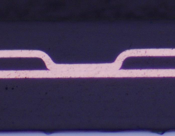
10 i3 Microsystems Overview Example of HSIP interconnect routing layers with nominal 18-micron lines, 25-micron via. The image is showing three routing layers. Typical completed HSIP wafer after 12 metal layers. 7 layers frontside, 5 layers backside. 10


11 i3 Microsystems Overview Die Harvesting Die Extraction & Recovery (DER) Services DER is available as a Foundry Service 11
12 i3 Microsystems Overview HSIP Reliability Baseline E-Test - Temperature Acceptance Test (ATP) PASS Temperature Shock MIL-STD-810G, Method 503.5, Procedure I-Steady State PASS Electrostatic Discharge EN , Level 4 PASS Electromagnetic Compatibility MIL-STD-461F,RE101,RE102 & Radiated Susceptibility PASS Mechanical Shock JEDEC Standard JESD22-B110A PASS Random Vibration MIL-STD-810G, Method 514.5; system operating during exposure PASS High Temperature MIL-STD-810G, Method 501.5; 2 day steady state +71 C PASS Low Temperature MIL-STD-810G, Method 502.5; 2 day steady state -35 C PASS Low Pressure (Altitude) MIL-STD-810G; system operating during exposure PASS Humidity MIL-STD-810G, Method system operating through test PASS Rain MIL-STD-810G, Method 506.5, device in system format PASS 1000 hours of HTOL at 125 degrees C PASS 1000 hours of THB at 85%, 85C PASS 2000 thermal cycles -29C to +85C PASS 12
13 i3 Electronics Overview 13

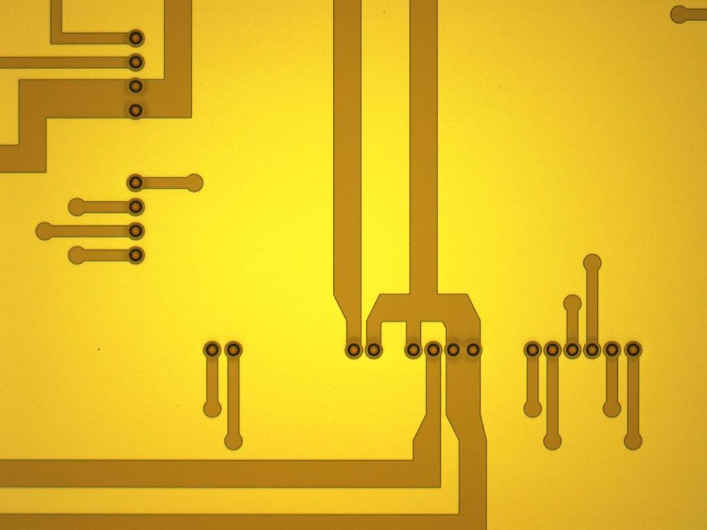
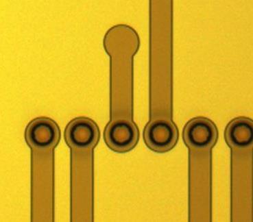
14 HSIP Fabrication HSIP Fabrication Discussion Target Component Target Component Detail view of HSIP module Layers 14
15 HSIP Fabrication Wafer Layout Detail R1C2 R1C3 R1C4 R2C1 R2C2 R2C3 R2C4 R2C5 R3C1 R3C2 R3C3 R3C4 R3C5 R4C1 R4C2 R4C3 R4C4 R4C5 R5C2 R5C3 R5C4 Percentage Metal Metal Layer of Module Area MCM_F_MET1 5.8% MCM_F_MET2 4.4% MCM_F_MET3 0.6% MCM_F_MET4 7.4% MCM_B_MET1 3.1% MCM_B_MET2 3.0% MCM_B_MET3 2.2% MCM_B_MET4 4.8% MCM_F_SM 2.2% MCM_B_SM 3.1% 100MM wafer with 21 Module positions 15.4 x 15.4 mm exposure field per module 13 embedded die per module (4 active) 4 metal layers per side (low density patterns) 15

 wafer over")
16 HSIP Fabrication Target Component Target Component Temporary Carrier Molded (Reconstituted) wafer over carrier actual wafer 16


17 HSIP Fabrication 2-micron copper Embedded die face 5-micron dielectric 2-micron copper 15-micron dielectric (3 Layers) 17
18 HSIP Fabrication Backside Wafer Thinning Opens the Thru-Via contacts Brings core of device to target value Target Component Temporary Carrier Target Component Completion of Backside Layers Temporary Carrier removed Device is singulated in normal dicing fashion Target Component Target Component 18


19 HSIP Fabrication Results Discussion of the actual ACT TA2 HSIP Build Results Georgia Tech BAE MMIC Fab i3 Microsystems HSIP Fab i3 Electronics Assembly Fab 19


20 HSIP Fabrication Results Die Shift from Wafer Molding GOOD RESULT NOT AS GOOD 20

21 HSIP Fabrication Results Fail Count R1C2 R1C3 R1C R2C1 R2C2 R2C3 R2C4 R2C R3C1 R3C2 R3C3 R3C4 R3C R4C1 R4C2 R4C3 R4C4 R4C R5C2 R5C3 R5C % Starting Yield Problem 21
22 HSIP Fabrication Results Wafer Level Die Shift AVG 48.7 STD 28 MAX MIN 6.8 BEFORE ADJUSTMENTS Wafer Level Die Shift AVG 9.2 STD 5.3 MAX 29.8 MIN 0.4 AFTER ADJUSTMENTS Recipe-controlled wafer molding process allows for optimization relative to placed die area and density 22
23 HSIP Fabrication Results 23

24 HSIP Fabrication Results Wafer ID Good Eng Scrap Wafer Yield % % % % Bin Yields 75% 11% 14% Across all 4 wafers and 32 metal layers, the yield was 75% for all visual non-conformances, including die shift 24
25 Particle_polymer Particle_unknown Other_no cat Void_encap Bubble_IV Particle_metallized Missing_other Extra_resist Damage_scratch Other_out of spec Extra_other Particle_fiber Extra_metal Cu Particle_metal Extra_IV Damage_other Void_other Encapsulation Bubble_other Missing_metal Particle_gooberx Bubble_resist Other_topo Damage_crack HSIP Fabrication Results Grand Total All Faults Pareto
26 FAULTS Other_no cat Damage_scratch Other_out of spec Encapsulation Missing_metal Particle_polymer Particle_unknown Bubble_IV Missing_other Particle_metallized Damage_other Particle_fiber Other_no cat Damage_scratch Other_out of spec Encapsulation Missing_metal Particle_polymer Particle_unknown Bubble_IV Missing_other Particle_metallized Damage_other Particle_fiber HSIP Fabrication Results Count of Status Status2 Status Conforming Faults Non-Conformances Grand Total Wafer Grand Total Count of Status Total Faults By Wafer Non-Conforming Module Faults Pareto Wafer Conforming Faults Non-Conformances Non-Conforming Faults Subcategory Gra die pad space_active space_inactive 1 1 trace_in via Grand Total
 Some etch process tuning remains for future wafer builds of this design")
27 HSIP Fabrication Results Etched Line Width Reduction (Delta to Design, all data in microns) Some etch process tuning remains for future wafer builds of this design 27
28 HSIP Fabrication Results Module Thickness Core (um) Module Thickness Total (um) Wafer Bond Module Date Wafer Module Thickness (um) Bow (um) XY Size (um) 6/13/2017 NPT /13/2017 NPT /13/2017 NPT /13/2017 NPT-001 6/13/2017 NPT-001 6/13/2017 NPT-002 R5C /13/2017 NPT-002 R4C /13/2017 NPT-002 R1C /13/2017 NPT-002 R2C /13/2017 NPT-002 R3C /24/2017 NPT-003 R1C /24/2017 NPT-003 R1C /24/2017 NPT-003 R3C /24/2017 NPT-003 R4C /24/2017 NPT-003 R4C /13/2017 NPT-004 R2C /13/2017 NPT-004 R2C /13/2017 NPT-004 R3C /13/2017 NPT-004 R4C /13/2017 NPT-004 R5C Final Module Bow Mean 14.5um Stdev 11.2um Final Module Thickness Mean 346.4um Stdev 7.0um Final Module Core Mean 270.5um Stdev 4.4um 28

29 HSIP Fabrication Results BAE MMIC die BAE MMIC gold pads i3 Microsystems Solder Mask i3 Electronics Solder i3 Microsystems UBM Cross-section of assembled stack, courtesy of i3 Electronics, 2017 i3 Microsystems copper pads 29
30 Conclusion HSIP technology can produce robust electronic components that meet next-generation packaging requirements for tightly packed integrations in order to achieve the lowest power, weight, and size while enabling new and exciting system concepts for designers THANK YOU 30
3D Integration Using Wafer-Level Packaging
 3D Integration Using Wafer-Level Packaging July 21, 2008 Patty Chang-Chien MMIC Array Receivers & Spectrographs Workshop Pasadena, CA Agenda Wafer-Level Packaging Technology Overview IRAD development on
Min Tao, Ph. D, Ashok Prabhu, Akash Agrawal, Ilyas Mohammed, Ph. D, Bel Haba, Ph. D Oct , IWLPC
 PACKAGE-ON-PACKAGE INTERCONNECT FOR FAN-OUT WAFER LEVEL PACKAGES Min Tao, Ph. D, Ashok Prabhu, Akash Agrawal, Ilyas Mohammed, Ph. D, Bel Haba, Ph. D Oct 18-20 2016, IWLPC 1 Outline Laminate to Fan-Out
Fraunhofer IZM - ASSID
 FRAUNHOFER-INSTITUT FÜR Zuverlässigkeit und Mikrointegration IZM Fraunhofer IZM - ASSID All Silicon System Integration Dresden Heterogeneous 3D Wafer Level System Integration 3D system integration is one
Adaptive Patterning. ISS 2019 January 8th
 Creating a system to balance natural variation ISS 2019 January 8th Tim Olson Founder & CTO Let s start with an industry perspective Historically, three distinct electronic industry silos Foundries SATS
Silicon Interposers enable high performance capacitors
 Interposers between ICs and package substrates that contain thin film capacitors have been used previously in order to improve circuit performance. However, with the interconnect inductance due to wire
Hermetic Packaging Solutions using Borosilicate Glass Thin Films. Lithoglas Hermetic Packaging Solutions using Borosilicate Glass Thin Films
 Hermetic Packaging Solutions using Borosilicate Glass Thin Films 1 Company Profile Company founded in 2006 ISO 9001:2008 qualified since 2011 Headquarters and Production in Dresden, Germany Production
TAIPRO Engineering. Speaker: M. Saint-Mard Managing director. TAIlored microsystem improving your PROduct
 TAIPRO Engineering MEMS packaging is crucial for system performance and reliability Speaker: M. Saint-Mard Managing director TAIPRO ENGINEERING SA Michel Saint-Mard Administrateur délégué m.saintmard@taipro.be
Fabricating 2.5D, 3D, 5.5D Devices
 Fabricating 2.5D, 3D, 5.5D Devices Bob Patti, CTO rpatti@tezzaron.com Tezzar on Semiconduct or 04/15/2013 1 Gen4 Dis-Integrated 3D Memory DRAM layers 42nm node 2 million vertical connections per lay per
The Future of Packaging ~ Advanced System Integration
 The Future of Packaging ~ Advanced System Integration Enabling a Microelectronic World R. Huemoeller SVP, Adv. Product / Platform Develop June 2013 Product Segments End Market % Share Summary 2 New Product
Session 4: Mixed Signal RF
 Sophia Antipolis October 5 th & 6 th 2005 Session 4: Mixed Signal RF Technology, Design and Manufacture of RF SiP Chris Barratt, Michel Beghin, Insight SiP Insight SiP Summary Introduction Definition of
Feature-level Compensation & Control
 Feature-level Compensation & Control 2 Sensors and Control Nathan Cheung, Kameshwar Poolla, Costas Spanos Workshop 11/19/2003 3 Metrology, Control, and Integration Nathan Cheung, UCB SOI Wafers Multi wavelength
Fan-Out Solutions: Today, Tomorrow the Future Ron Huemoeller
 Fan-Out Solutions: Today, Tomorrow the Future Ron Huemoeller Corporate Vice President, WW RnD & Technology Strategy 1 In the Beginning ewlb 2 Fan Out Packaging Emerges Introduction of Fan Out (ewlb) Marketed
Laminate Based Fan-Out Embedded Die Technologies: The Other Option
 Laminate Based Fan-Out Embedded Die Technologies: The Other Option Theodore (Ted) G. Tessier, Tanja Karila*, Tuomas Waris*, Mark Dhaenens and David Clark FlipChip International, LLC 3701 E University Drive
Brief Introduction of Sigurd IC package Assembly
 Brief Introduction of Sigurd IC package Assembly Content Package Development Trend Product Brief Sawing type QFN Representative MEMS Product LGA Light Sensor Proximity Sensor High Yield Capability Low
3D TSV Micro Cu Column Chip-to-Substrate/Chip Assmbly/Packaging Technology
 3D TSV Micro Cu Column Chip-to-Substrate/Chip Assmbly/Packaging Technology by Seung Wook Yoon, *K. T. Kang, W. K. Choi, * H. T. Lee, Andy C. B. Yong and Pandi C. Marimuthu STATS ChipPAC LTD, 5 Yishun Street
TSV MEOL (Mid-End-Of-Line) and its Assembly/Packaging Technology for 3D/2.5D Solutions
 and its Assembly/Packaging Technology for 3D/2.5D Solutions") TSV MEOL (Mid-End-Of-Line) and its Assembly/Packaging Technology for 3D/2.5D Solutions Seung Wook YOON, D.J. Na, *K. T. Kang, W. K. Choi, C.B. Yong, *Y.C. Kim and Pandi C. Marimuthu STATS ChipPAC Ltd.
TSV MEOL (Mid-End-Of-Line) and its Assembly/Packaging Technology for 3D/2.5D Solutions Seung Wook YOON, D.J. Na, *K. T. Kang, W. K. Choi, C.B. Yong, *Y.C. Kim and Pandi C. Marimuthu STATS ChipPAC Ltd.
450mm and Moore s Law Advanced Packaging Challenges and the Impact of 3D
 450mm and Moore s Law Advanced Packaging Challenges and the Impact of 3D Doug Anberg VP, Technical Marketing Ultratech SOKUDO Lithography Breakfast Forum July 10, 2013 Agenda Next Generation Technology
SAMPLE SLIDES & COURSE OUTLINE. Core Competency In Semiconductor Technology: 2. FABRICATION. Dr. Theodore (Ted) Dellin
 Dellin") & Digging Deeper Devices, Fabrication & Reliability For More Info:.com or email Dellin@ieee.org SAMPLE SLIDES & COURSE OUTLINE In : 2. A Easy, Effective, of How Devices Are.. Recommended for everyone who
& Digging Deeper Devices, Fabrication & Reliability For More Info:.com or email Dellin@ieee.org SAMPLE SLIDES & COURSE OUTLINE In : 2. A Easy, Effective, of How Devices Are.. Recommended for everyone who
Intel's 65 nm Logic Technology Demonstrated on 0.57 µm 2 SRAM Cells
 Intel's 65 nm Logic Technology Demonstrated on 0.57 µm 2 SRAM Cells Mark Bohr Intel Senior Fellow Director of Process Architecture & Integration Intel 1 What are We Announcing? Intel has fabricated fully-functional
8-18 GHz Wideband Low Noise Amplifier
 8-18 GHz Wideband Low Noise Amplifier Features Frequency Range : 8.0 18.0GHz 23dB Nominal gain Low Midband Noise Figure < 2 db Input Return Loss > 12 db Output Return Loss > 12 db Single +3V Operation
UMS User guide for bare dies GaAs MMIC. storage, pick & place, die attach and wire bonding
 UMS User guide for bare dies GaAs MMIC storage, pick & place, die attach and wire bonding Ref. : AN00014097-07 Apr 14 1/10 Specifications subject to change without notice United Monolithic Semiconductors
9-10 GHz LOW NOISE AMPLIFIER
 9-10 GHz LOW NOISE AMPLIFIER Features Frequency Range 9-10GHz Low Noise Figure < 1.38 db High Gain 28 ± 0.4dB Input Return Loss > 10dB. Output Return Loss > 13dB. 10 dbm is Nominal P1dB 20 dbm OIP3 No
Flip-Chip for MM-Wave and Broadband Packaging
 1 Flip-Chip for MM-Wave and Broadband Packaging Wolfgang Heinrich Ferdinand-Braun-Institut für Höchstfrequenztechnik (FBH) Berlin / Germany with contributions by F. J. Schmückle Motivation Growing markets
MICROELECTRONICS ASSSEMBLY TECHNOLOGIES. The QFN Platform as a Chip Packaging Foundation
 West Coast Luncheon January 15, 2014. PROMEX PROMEX INDUSTRIES INC. MICROELECTRONICS ASSSEMBLY TECHNOLOGIES The QFN Platform as a Chip Packaging Foundation 3075 Oakmead Village Drive Santa Clara CA Ɩ 95051
Flexible Hybrid Electronics Fabricated with High-Performance COTS ICs using RTI CircuitFilm TM Technology
 Flexible Hybrid Electronics Fabricated with High-Performance COTS ICs using RTI CircuitFilm TM Technology Scott Goodwin 1, Erik Vick 2 and Dorota Temple 2 1 Micross Advanced Interconnect Technology Micross
Integration of 3D detector systems
 Integration of 3D detector systems Piet De Moor Introduction Evolution in radiation detection/imaging: single pixel linear array 2D array increase in resolution = decrease in pitch (down to few um) = thanks
Enabling concepts: Packaging Technologies
 Enabling concepts: Packaging Technologies Ana Collado / Liam Murphy ESA / TEC-EDC 01/10/2018 ESA UNCLASSIFIED - For Official Use Enabling concepts: Packaging Technologies Drivers for the future: Higher
Packaging Roadmap: The impact of miniaturization. Bob Pfahl, inemi Celestica-iNEMI Technology Forum May 15, 2007
 Packaging Roadmap: The impact of miniaturization Bob Pfahl, inemi Celestica-iNEMI Technology Forum May 15, 2007 The Challenges for the Next Decade Addressing the consumer experience using the converged
TGP GHz 180 Phase Shifter. Primary Applications. Product Description. Measured Performance
 Amplitude Error (db) S21 (db) 10.0 9.0 8.0 7.0 6.0 5.0 4.0 3.0 2.0 1.0 Measured Performance 0.0 140 30 31 32 33 34 35 36 37 38 39 40 0-1 -2-3 -4-5 State 0-6 State 1-7 -8-9 -10 30 31 32 33 34 35 36 37 38
MicroSiP TM DC/DC Converters Fully Integrated Power Solutions
 MicroSiP TM DC/DC Converters Fully Integrated Power Solutions PicoStar TM Christophe Vaucourt Thies Puchert, Udo Ottl, Frank Stepniak, Florian Feckl 1 Outline Illustrate TI s recent developments in the
Advanced Wafer Level Packaging of RF-MEMS with RDL Inductor
 Advanced Wafer Level Packaging of RF-MEMS with RDL Inductor Paul Castillou, Roberto Gaddi, Rob van Kampen, Yaojian Lin*, Babak Jamshidi** and Seung Wook Yoon*** Cavendish Kinetics, 2960 North First Street,
6-13 GHz Low Noise Amplifier TGA8399B-SCC
 6-13 GHz Low Noise Amplifier Key Features and Performance 6-13 GHz Frequency Range 1.5 db Typical Noise Figure Midband 26 db Nominal Gain High Input Power Handling: ~ 20dBm Balanced Input for Low VSWR
Manufacturing Development of a New Electroplated Magnetic Alloy Enabling Commercialization of PwrSoC Products
 Manufacturing Development of a New Electroplated Magnetic Alloy Enabling Commercialization of PwrSoC Products Trifon Liakopoulos, Amrit Panda, Matt Wilkowski and Ashraf Lotfi PowerSoC 2012 CONTENTS Definitions
CMP for Advanced Packaging
 CMP for Advanced Packaging Robert L. Rhoades, Ph.D. NCCAVS TFUG-CMPUG Joint Meeting June 9, 2016 Semiconductor Equipment Spare Parts and Service CMP Foundry Foundry Click to edit Master Outline title style
The Design Challenge to Integrate High Performance Organic Packaging into High End ASIC Strategic Space Based Applications.
 The Design Challenge to Integrate High Performance Organic Packaging into High End ASIC Strategic Space Based Applications May 8, 2007 Abstract: The challenge to integrate high-end, build-up organic packaging
Application Bulletin 240
 Application Bulletin 240 Design Consideration CUSTOM CAPABILITIES Standard PC board fabrication flexibility allows for various component orientations, mounting features, and interconnect schemes. The starting
3D ICs: Recent Advances in the Industry
 3D ICs: Recent Advances in the Industry Suresh Ramalingam Senior Director, Advanced Packaging Outline 3D IC Background 3D IC Technology Development Summary Acknowledgements Stacked Silicon Interconnect
TGA2509. Wideband 1W HPA with AGC
 Product Description The TriQuint TGA2509 is a compact Wideband High Power Amplifier with AGC. The HPA operates from 2-22 GHz and is designed using TriQuint s proven standard 0.25 um gate phemt production
New Wave SiP solution for Power
 New Wave SiP solution for Power Vincent Lin Corporate R&D ASE Group APEC March 7 th, 2018 in San Antonio, Texas. 0 Outline Challenges Facing Human Society Energy, Environment and Traffic Autonomous Driving
Market and technology trends in advanced packaging
 Close Market and technology trends in advanced packaging Executive OVERVIEW Recent advances in device miniaturization trends have placed stringent requirements for all aspects of product manufacturing.
Recent Developments in Multifunctional Integration. Stephan Guttowski, Head of Technology Park»Heterointegration«, Fraunhofer FMD
 Recent Developments in Multifunctional Integration Stephan Guttowski, Head of Technology Park»Heterointegration«, Fraunhofer FMD Founding Participants 2 One-Stop-Shop for developments from wafer technologies
Ka-Band 2W Power Amplifier
 Ka-Band 2W Power Amplifier Key Features 30-40 GHz Bandwidth > 33 dbm Nominal Psat @ Pin = 20dBm 18 db Nominal Gain Bias: 6 V, 50 ma Idq (1.9A under RF Drive) 0.15 um 3MI MMW phemt Technology Thermal Spreader
50 Micron Pitch Flip Chip Bumping Technology: Processes and Applications
 50 Micron Pitch Flip Chip Bumping Technology: Processes and Applications Alan Huffman Center for Materials and Electronic Technologies huffman@rti.org Outline RTI Identity/History Historical development
33-47 GHz Wide Band Driver Amplifier TGA4522
 33-47 GHz Wide Band Driver Amplifier Key Features Frequency Range: 33-47 GHz 27.5 dbm Nominal Psat @ 38GHz 27 dbm P1dB @ 38 GHz 36 dbm OTOI @ Pin = 19 dbm/tone 18 db Nominal Gain @ 38GHz db Nominal Return
New Approaches to Develop a Scalable 3D IC Assembly Method
 New Approaches to Develop a Scalable 3D IC Assembly Method Charles G. Woychik Ph.D. Sangil Lee, Ph.D., Scott McGrath, Eric Tosaya and Sitaram Arkalgud Ph.D. Invensas Corporation 3025 Orchard Parkway San
17-43 GHz MPA / Multiplier. S-Parameters (db) P1dB (dbm)
 P1dB (dbm)") 17-43 GHz MPA / Multiplier Key Features Frequency: 17-43 GHz 25 db Nominal Gain @ Mid-band 22 dbm Nominal Output P1dB 2x and 3x Multiplier Function.15 um 3MI phemt Technology Chip Dimensions 1.72 x.76
17-43 GHz MPA / Multiplier Key Features Frequency: 17-43 GHz 25 db Nominal Gain @ Mid-band 22 dbm Nominal Output P1dB 2x and 3x Multiplier Function.15 um 3MI phemt Technology Chip Dimensions 1.72 x.76
Plan Optik AG. Plan Optik AG PRODUCT CATALOGUE
 Plan Optik AG Plan Optik AG PRODUCT CATALOGUE 2 In order to service the high demand of wafers more quickly, Plan Optik provides off the shelf products in sizes from 2 up to 300mm diameter. Therefore Plan
2 40 GHz Ultra-Wideband Amplifier
 AMT217511 Rev. 1. January 28 2 4 GHz Ultra-Wideband Amplifier Features Frequency Range: 2-4 GHz 7±1. db Nominal Gain Input Return Loss > 1 db Output Return Loss > 1 db Reverse Isolation > 3dB 5 dbm Nominal
Advanced High-Density Interconnection Technology
 Advanced High-Density Interconnection Technology Osamu Nakao 1 This report introduces Fujikura s all-polyimide IVH (interstitial Via Hole)-multi-layer circuit boards and device-embedding technology. Employing
23-29 GHz High Power Amplifier TGA9070-SCC
 23-29 GHz High Power Amplifier TGA9070-SCC Description The TriQuint TGA9070-SCC is a three stage HPA MMIC design using TriQuint s proven 0.25 um Power phemt process to support a variety of millimeter wave
3D Integration developments & manufacturing CEA-LETI. D. Henry CEA-Leti-Minatec
 3D Integration developments & manufacturing offer @ CEA-LETI D. Henry CEA-Leti-Minatec Outline Introduction 3D Integration R&D activities overview 3D integration Manufacturing offer : Open 3D platform
First Demonstration of Panel Glass Fan-out (GFO) Packages for High I/O Density and High Frequency Multi-Chip Integration
 Packages for High I/O Density and High Frequency Multi-Chip Integration") First Demonstration of Panel Glass Fan-out (GFO) Packages for High I/O Density and High Frequency Multi-Chip Integration Tailong Shi, Chintan Buch,Vanessa Smet, Yoichiro Sato, Lutz Parthier, Frank Wei
First Demonstration of Panel Glass Fan-out (GFO) Packages for High I/O Density and High Frequency Multi-Chip Integration Tailong Shi, Chintan Buch,Vanessa Smet, Yoichiro Sato, Lutz Parthier, Frank Wei
Through Glass Via (TGV) Technology for RF Applications
 Technology for RF Applications") Through Glass Via (TGV) Technology for RF Applications C. H. Yun 1, S. Kuramochi 2, and A. B. Shorey 3 1 Qualcomm Technologies, Inc. 5775 Morehouse Dr., San Diego, California 92121, USA Ph: +1-858-651-5449,
Through Glass Via (TGV) Technology for RF Applications C. H. Yun 1, S. Kuramochi 2, and A. B. Shorey 3 1 Qualcomm Technologies, Inc. 5775 Morehouse Dr., San Diego, California 92121, USA Ph: +1-858-651-5449,
2D to 3d architectures: back to the future
 2D to 3d architectures: back to the future Raja Swaminathan Package architect Intel Corporation 2018 IMAPS Device Packaging Keynote, 03/06/2018 acknowledgements Ravi Mahajan, Ram Viswanath, Bob Sankman,
GHz Voltage Variable Attenuator (Absorptive)
") Rev.. February 27.5-2.GHz Voltage Variable Attenuator (Absorptive) Features Single Positive Voltage Control: to +5V. 3dB Attenuation Range Low Insertion Loss I/O VSWR
Rev.. February 27.5-2.GHz Voltage Variable Attenuator (Absorptive) Features Single Positive Voltage Control: to +5V. 3dB Attenuation Range Low Insertion Loss I/O VSWR
IMAGE SENSOR EVOLUTION AND ENABLING 3D TECHNOLOGIES
 Fig. 5: Scanning Electron Microscopy images (TOP view, 3D view, Zoome including all metal levels of the BSI imager structure. (dashed line shows bonding IMAGE SENSOR EVOLUTION AND ENABLING 3D TECHNOLOGIES
TechSearch International, Inc. Corporate Overview E. Jan Vardaman, President
 TechSearch International, Inc. Corporate Overview E. Jan Vardaman, President Corporate Background Founded in 1987 and headquartered in Austin, Texas Recognized around the world as a leading consulting
Inductors In Silicon Based on SU-8 Enhanced Silicon Molding Technique for Portable Electronics
 Biophotonics & Microsystems Lab Inductors In Silicon Based on SU-8 Enhanced Silicon Molding Technique for Portable Electronics Mingliang Wang 1*, Khai D. T. Ngo 2, Huikai Xie 1 1 BML, University of Florida
Stack Die CSP Interconnect Challenges Flynn Carson, Glenn Narvaez, HC Choi, and DW Son ChipPAC, Inc.
 Stack Die CSP Interconnect Challenges Flynn Carson, Glenn Narvaez, HC Choi, and DW Son ChipPAC, Inc. IEEE/CPMT Seminar Overview 4 Stacked die Chip Scale Packages (CSPs) enable more device functionality
Fiber Optics for Harsh Environments ICSO Chuck Tabbert
 Fiber Optics for Harsh Environments ICSO 2016 Chuck Tabbert VP Sales & Marketing Ultra Communications (505) 823-1293 ctabbert@ultracomm-inc.com www.ultracomm-inc.com If anyone would like copy of briefing
The 3D Silicon Leader
 The 3D Silicon Leader 3D Silicon IPD for smaller and more reliable Implantable Medical Devices ATW on Advanced Packaging for Wireless Medical Devices Mohamed Mehdi Jatlaoui, Sébastien Leruez, Olivier Gaborieau,
TGA2521-SM GHz Linear Driver Amplifier Key Features Measured Performance
 17-24 GHz Linear Driver Amplifier Key Features Frequency Range: 17-24 GHz 25.5 dbm Nominal Psat, 23.5 dbm Nominal P1dB Gain: 20 db OTOI: 33 dbm Typical Bias: Vd = 5 V, Idq = 320 ma, Vg = -0.5 V Typical
Reliability Qualification Report
 Reliability Qualification Report SGA-5263Z Products Qualified by Similarity SGA-4563Z/4463Z/4363Z/4263Z/4163Z SGA-3563Z/3463Z/3363Z/3263Z SGA-2463Z/2363Z/2263Z/2163Z SGA-1263Z/1163Z SGA-0363Z/0163Z SGA-8343Z/8543Z
An Introduction to Electronics Systems Packaging. Prof. G. V. Mahesh. Department of Electronic Systems Engineering
 An Introduction to Electronics Systems Packaging Prof. G. V. Mahesh Department of Electronic Systems Engineering India Institute of Science, Bangalore Module No. # 02 Lecture No. # 08 Wafer Packaging Packaging
2-18 GHz Low Noise Amplifier TGA8344-SCC
 April 3, 2003 2-18 GHz Low Noise Amplifier Key Features and Performance 2 to 18 GHz Frequency Range Typical 4 db Noise Figure at Midband 16 dbm Typical Output Power at 1 db Gain Compression 19 db Typical
MAAL DIESMB. Low Noise Amplifier DC - 28 GHz. Features. Functional Schematic 1. Description. Pin Configuration 2. Ordering Information. Rev.
 MAAL-11141-DIE Features Ultra Wideband Performance Noise Figure: 1.4 db @ 8 GHz High Gain: 17 db @ 8 GHz Output IP3: 28 dbm @ 8 GHz Bias Voltage: V DD = - V Bias Current: I DSQ = 6 - ma Ω Matched Input
Jan Bogaerts imec
 imec 2007 1 Radiometric Performance Enhancement of APS 3 rd Microelectronic Presentation Days, Estec, March 7-8, 2007 Outline Introduction Backside illuminated APS detector Approach CMOS APS (readout)
POSSUM TM Die Design as a Low Cost 3D Packaging Alternative
 POSSUM TM Die Design as a Low Cost 3D Packaging Alternative The trend toward 3D system integration in a small form factor has accelerated even more with the introduction of smartphones and tablets. Integration
Innovations Push Package-on-Package Into New Markets. Flynn Carson. STATS ChipPAC Inc Kato Rd Fremont, CA 94538
 Innovations Push Package-on-Package Into New Markets by Flynn Carson STATS ChipPAC Inc. 47400 Kato Rd Fremont, CA 94538 Copyright 2010. Reprinted from Semiconductor International, April 2010. By choosing
17-24 GHz Linear Driver Amplifier. S11 and S22 (db) -15
 -15") Pout (dbm) or OTOI (dbm) S21 (db) S11 and S22 (db) 17-24 GHz Linear Driver Amplifier Key Features Frequency Range: 17-24 GHz 25.5 dbm Nominal Psat, 23.5 dbm Nominal P1dB Gain: 20 db OTOI: 33 dbm Typical
Pout (dbm) or OTOI (dbm) S21 (db) S11 and S22 (db) 17-24 GHz Linear Driver Amplifier Key Features Frequency Range: 17-24 GHz 25.5 dbm Nominal Psat, 23.5 dbm Nominal P1dB Gain: 20 db OTOI: 33 dbm Typical
CREATING RELIABLE AND MANUFACTURABLE RF DESIGNS
 CREATING RELIABLE AND MANUFACTURABLE RF DESIGNS Chandra Gupta, Ph.D., MBA CPI, BMD, Beverly, MA IEEE Boston Reliability Chapter, Lexington, MA Sept 13, 2017 IEEE Boston Reliability Boston Chapter Sept
Mobile Electrostatic Carrier (MEC) evaluation for a GaAs wafer backside manufacturing process
 evaluation for a GaAs wafer backside manufacturing process") Mobile Electrostatic Carrier (MEC) evaluation for a GaAs wafer backside manufacturing process H.Stieglauer 1, J.Nösser 1, A.Miller 1, M.Lanz 1, D.Öttlin 1, G.Jonsson 1, D.Behammer 1, C.Landesberger 2,
Mobile Electrostatic Carrier (MEC) evaluation for a GaAs wafer backside manufacturing process H.Stieglauer 1, J.Nösser 1, A.Miller 1, M.Lanz 1, D.Öttlin 1, G.Jonsson 1, D.Behammer 1, C.Landesberger 2,
Data Sheet _ R&D. Rev Date: 8/17
 Data Sheet _ R&D Rev Date: 8/17 Micro Bump In coming years the interconnect density for several applications such as micro display, imaging devices will approach the pitch 10um and below. Many research
Substrates Lost in Translation
 2004 IEEE PRESENTATION Components, Packaging & Manufacturing Technology (CPMT) Society, Santa Clara Valley Chapter www.cpmt.org/scv/ Substrates Lost in Translation R. Huemoeller Vice President, Substrate
PH9 Reliability. Application Note # 51 - Rev. A. MWTC MARKETING March 1997
 PH9 Reliability Application Note # 51 - Rev. A MWTC MARKETING March 1997 1.0. Introduction This application note provides a summary of reliability and environmental testing performed to date on 0.25 µm
Integrated Photonics using the POET Optical InterposerTM Platform
 Integrated Photonics using the POET Optical InterposerTM Platform Dr. Suresh Venkatesan CIOE Conference Shenzhen, China Sept. 5, 2018 POET Technologies Inc. TSXV: PUBLIC POET PTK.V Technologies Inc. PUBLIC
Silicon carbide Semiconductor Products
 Power Matters. Silicon carbide Semiconductor Products Low Switching Losses High Power Density High Thermal Conductivity Reduced Heat Sink Requirements High Temperature Operation Reduced Circuit Size and
18-40 GHz Low Noise Amplifier
 18-40 GHz Low Noise Amplifier AMT2172011 Features Frequency Range: 18-40 GHz Better than 4.5 db Noise Figure Single supply operation DC decoupled Input and Output 10 db Nominal Gain 6dBm Nominal P1dB Input
Parameter Min Typ Max Units Frequency Range
 Features Low loss broadband performance High isolation Fast switching speed Non-reflective design - RF1 and RF2 Small die size Description Functional Block Diagram RF1 RF2 1 2 The CMD204 die is a general
RF1. Parameter Min Typ Max Units Frequency Range
 Features Functional Block Diagram Low loss broadband performance High isolation Fast switching speed Reflective design Small die size Description RFC 1 The CMD230 is a general purpose broadband high isolation
TGV2204-FC. 19 GHz VCO with Prescaler. Key Features. Measured Performance. Primary Applications Automotive Radar. Product Description
 19 GHz VCO with Prescaler Key Features Frequency Range: 18.5 19.5 GHz Output Power: 7 dbm @ 19 GHz Phase Noise: -105 dbc/hz at 1 MHz offset, fc=19 GHz Prescaler Output Freq Range : 2.31 2.44 GHz Prescaler
LED Cost and Technology Trends: How to enable massive adoption in general lighting
 LED Cost and Technology Trends: How to enable massive adoption in general lighting SEMICON West 2011 Moscone Center, San Francisco June 13 th 2011 Lumileds Lumileds OSRAM Aixtron CREE OSRAM OKI OSRAM 45
12-18 GHz Ku-Band 3-Stage Driver Amplifier TGA2507
 12- GHz Ku-Band 3-Stage Driver Amplifier Key Features 12- GHz Bandwidth 28 db Nominal Gain dbm P1dB Bias: 5,6,7 V, 80 ± 10% ma Self Bias 0.5 um 3MI mmw phemt Technology Chip Dimensions: 1.80 x 0.83 x 0.1
Parameter Min Typ Max Units Frequency Range
 Features Low loss broadband performance High isolation Fast switching speed Non-reflective design Small die size Functional Block Diagram B A 3 4 5 2 RFC A B 6 Description The CMD196 is a general purpose
Flexline - A Flexible Manufacturing Method for Wafer Level Packages (Extended Abstract)
") Flexline - A Flexible Manufacturing Method for Wafer Level Packages (Extended Abstract) by Tom Strothmann, *Damien Pricolo, **Seung Wook Yoon, **Yaojian Lin STATS ChipPAC Inc.1711 W Greentree Drive Tempe,
Flexline - A Flexible Manufacturing Method for Wafer Level Packages (Extended Abstract) by Tom Strothmann, *Damien Pricolo, **Seung Wook Yoon, **Yaojian Lin STATS ChipPAC Inc.1711 W Greentree Drive Tempe,
TGA2521-SM GHz Linear Driver Amplifier. Key Features. Measured Performance
 17-24 GHz Linear Driver Amplifier Key Features Frequency Range: 17-24 GHz 25.5 dbm Nominal Psat, 23.5 dbm Nominal P1dB Gain: 20 db OTOI: 33 dbm Typical Bias: Vd = 5 V, Idq = 320 ma, Vg = -0.5 V Typical
Application Note 5011
 MGA-62563 High Performance GaAs MMIC Amplifier Application Note 511 Application Information The MGA-62563 is a high performance GaAs MMIC amplifier fabricated with Avago Technologies E-pHEMT process and
Analog Devices Welcomes Hittite Microwave Corporation NO CONTENT ON THE ATTACHED DOCUMENT HAS CHANGED
 Analog Devices Welcomes Hittite Microwave Corporation NO CONTENT ON THE ATTACHED DOCUMENT HAS CHANGED www.analog.com www.hittite.com Report Title: Report Type: Date: Qualification Test Report See Attached
Application Note 5012
 MGA-61563 High Performance GaAs MMIC Amplifier Application Note 5012 Application Information The MGA-61563 is a high performance GaAs MMIC amplifier fabricated with Avago Technologies E-pHEMT process and
High Frequency Single & Multi-chip Modules based on LCP Substrates
 High Frequency Single & Multi-chip Modules based on Substrates Overview Labtech Microwave has produced modules for MMIC s (microwave monolithic integrated circuits) based on (liquid crystal polymer) substrates
TGA2521-SM GHz Linear Driver Amplifier. Key Features. Measured Performance
 17-24 GHz Linear Driver Amplifier Key Features Frequency Range: 17-24 GHz 25.5 dbm Nominal Psat, 23.5 dbm Nominal P1dB Gain: 20 db OTOI: 33 dbm Typical Bias: Vd = 5 V, Idq = 320 ma, Vg = -0.5 V Typical
!"#$"%&' ()#*+,-+.&/0(
#*+,-+.&/0(") !"#$"%&' ()#*+,-+.&/0( Multi Chip Modules (MCM) or Multi chip packaging Industry s first MCM from IBM. Generally MCMs are horizontal or two-dimensional modules. Defined as a single unit containing two
!"#$"%&' ()#*+,-+.&/0( Multi Chip Modules (MCM) or Multi chip packaging Industry s first MCM from IBM. Generally MCMs are horizontal or two-dimensional modules. Defined as a single unit containing two
Lecture: Integration of silicon photonics with electronics. Prepared by Jean-Marc FEDELI CEA-LETI
 Lecture: Integration of silicon photonics with electronics Prepared by Jean-Marc FEDELI CEA-LETI Context The goal is to give optical functionalities to electronics integrated circuit (EIC) The objectives
Product Catalog. Semiconductor Intellectual Property & Technology Licensing Program
 Product Catalog Semiconductor Intellectual Property & Technology Licensing Program MANUFACTURING PROCESS TECHNOLOGY OVERVIEW 90 nm 130 nm 0.18 µm 0.25 µm 0.35 µm >0.40 µm Logic CMOS SOI CMOS SOI CMOS SOI
CMD282. DC-40 GHz 2-bit Digital Attenuator. Features. Functional Block Diagram. Description
 Features Functional Block Diagram Ultra wideband performance Low insertion loss Wide attenuation range Small die size Description The CMD282 is negative controlled, wideband GaAs MMIC 2-bit digital attenuator
Application Note 5351
 AMMP-6408 Thermal Application Examples Application Note 5351 Introduction The AMMP-6408 is a 1 W power amplifier operating over the 6 to 18 GHz frequency range and is housed in a 5 x 5 mm surface mount
64 Channel Flip-Chip Mounted Selectively Oxidized GaAs VCSEL Array
 64 Channel Flip-Chip Mounted Selectively Oxidized GaAs VCSEL Array 69 64 Channel Flip-Chip Mounted Selectively Oxidized GaAs VCSEL Array Roland Jäger and Christian Jung We have designed and fabricated
Modeling, Design, and Demonstration of 2.5D Glass Interposers for 16-Channel 28 Gbps Signaling Applications
 Modeling, Design, and Demonstration of 2.5D Glass Interposers for 16-Channel 28 Gbps Signaling Applications Brett Sawyer, Bruce C. Chou, Saumya Gandhi, Jack Mateosky, Venky Sundaram, and Rao Tummala 3D
MEMS in ECE at CMU. Gary K. Fedder
 MEMS in ECE at CMU Gary K. Fedder Department of Electrical and Computer Engineering and The Robotics Institute Carnegie Mellon University Pittsburgh, PA 15213-3890 fedder@ece.cmu.edu http://www.ece.cmu.edu/~mems
CMD GHz Active Frequency Doubler. Features. Functional Block Diagram. Description
 Features Functional Block Diagram High output power Excellent Fo isolation Broadband performance Small die size Description The CMD214 die is a broadband MMIC GaAs x2 active frequency multiplier. When