FPGA Based System Design
|
|
|
- Shon Bryant
- 6 years ago
- Views:
Transcription
1 FPGA Based System Design
2 Reference Wayne Wolf, FPGA-Based System Design Pearson Education, 2004
3 Why VLSI? Integration improves the design: higher speed; lower power; physically smaller. Integration reduces manufacturing cost (almost) - no manual assembly.
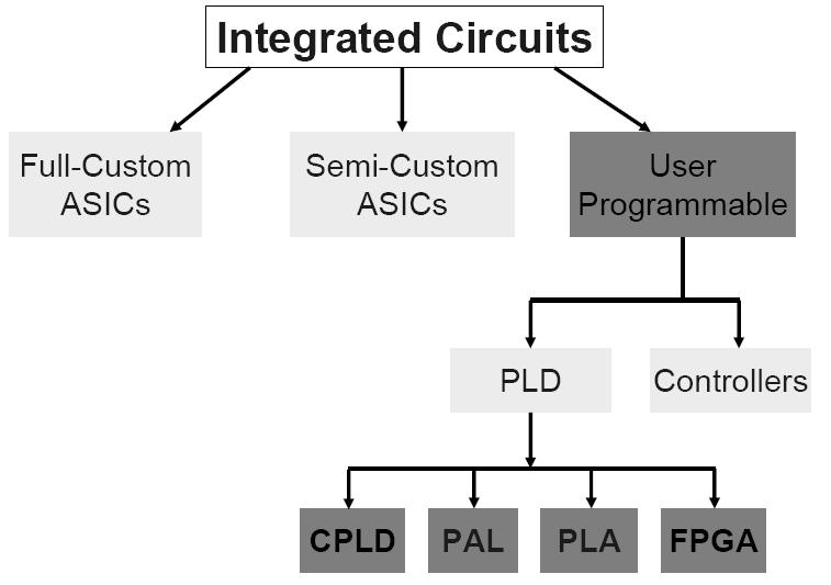
4 Integrated Circuits
5 Full Custom ICs Can achieve very high transistor density (transistors per square micron) design time can be very long (multiple months). Involves the creation of a completely new chip, which consists of masks (for the photolithographic manufacturing process) Benefits - Excellent performance, small size, low power
6 Standard Cell Designer uses a library of standard cells an automatic place and route tool does the layout Transistor density and performance degradation depends on type of design being done. Design time can be much faster than full custom because layout is automatically generated.

7 Gate Array Designer uses a library of standard cells. The design is mapped onto an array of transistors which is already created on a wafer wafers with transistor arrays can be created ahead of time A routing tool creates the masks for the routing layers and "customizes" the pre-created gate array for the user's design Transistor density can be almost as good as standard cell. Design time advantages are the same as for standard cell.
8 Semi-custom ICs Flexible as portion of the IC is customized by the user Suitable for specific applications Gate array + standard cell Paves way for application specific ICs (ASIC)
9 Role of FPGA Microprocessors used in variety of environments Rely on software to implement functions Generally slower and more power-hungry than custom chips When FPGAs? Design economics Shortest time to market Lowest NRE cost Highest unit cost Make quick grab for market share Same FPGA reused in several designs
10 Programmable logic devices Programmable Logic Device (PLD): An integrated circuit chip that can be configured by end user to implement different digital hardware Also known as Field Programmable Logic Device (FPLD)
11 PLD PLD as a Black Box Inputs (logic variables) Logic gates and programmable switches Outputs (logic functions)
12 Programmable Logic Array (PLA) x 1 x 2 x n Use to implement circuits in SOP form The connections in the AND plane are programmable Input buffers and inverters x 1 x 1 x n x n The connections in the OR plane are programmable AND plane P 1 P k OR plane f 1 f m
13 Gate Level Version of PLA x 1 x 2 x 3 f 1 = x 1 x 2 +x 1 x 3 '+x 1 'x 2 'x 3 P 1 Programmable connections OR plane f 2 = x 1 x 2 +x 1 'x 2 'x 3 +x 1 x 3 P 2 P 3 P 4 AND plane f 1 f 2
14 Customary Schematic of a PLA x 1 x 2 x 3 f 1 = x 1 x 2 +x 1 x 3 '+x 1 'x 2 'x 3 f 2 = x 1 x 2 +x 1 'x 2 'x 3 +x 1 x 3 P 1 OR plane P 2 P 3 P 4 x marks the connections left in place after programming AND plane f 1 f 2
15 Limitations of PLAs Typical size is 16 inputs, 32 product terms, 8 outputs Each AND gate has large fan-in - this limits the number of inputs that can be provided in a PLA 16 inputs 2 16 = possible input combinations; only 32 permitted (since 32 AND gates) in a typical PLA 32 AND terms permitted large fan-in for OR gates as well This makes PLAs slower and slightly more expensive than some alternatives to be discussed shortly
16 Programmable ROM (PROM) N input 2 N x M ROM M output Address: N bits; Output word: M bits ROM contains 2 N words of M bits each The input bits decide the particular word that becomes available on output lines 16
17 Logic Diagram of 8x3 PROM Sum of minterms 17
18 Combinational Circuit Implementation using PROM I0 I1 I2 F0 F1 F F0 F1 F2 18
19 PROM Types Programmable PROM Break links through current pulses Write once, Read multiple times Erasable PROM (EPROM) Program with ultraviolet light Write multiple times, Read multiple times Electrically Erasable PROM (EEPROM)/ Flash Memory Program with electrical signal Write multiple times, Read multiple times 19
20 PROM: Advantages and Disadvantages Widely used to implement functions with large number of inputs and outputs For combinational circuits with lots of don t care terms, PROM is a wastage of logic resources 20
21 Programmable Array Logic (PAL) x 1 x 2 x n Also used to implement circuits in SOP form The connections in the AND plane are programmable x 1 x 1 Input buffers and inverters x n x n fixed connections The connections in the OR plane are NOT programmable AND plane P 1 P k OR plane f 1 f m
22 Example Schematic of a PAL x 1 x 2 x 3 f 1 = x 1 x 2 x 3 '+x 1 'x 2 x 3 f 2 = x 1 'x 2 '+x 1 x 2 x 3 P 1 P 2 f 1 P 3 P 4 f 2 AND plane
23 Comparing PALs and PLAs PALs have the same limitations as PLAs (small number of allowed AND terms) plus they have a fixed OR plane less flexibility than PLAs PALs are simpler to manufacture, cheaper, and faster (better performance) PALs also often have extra circuitry connected to the output of each OR gate The OR gate plus this circuitry is called a macrocell
24 Macrocell OR gate from PAL Select 0 1 Enable f 1 Clock D Q Flip-flop back to AND plane
25 Macrocell Functions Enable = 0 can be used to allow the output pin for f 1 to be used as an additional input pin to the PAL Enable = 1, Select = 0 is normal for typical PAL operation Select 0 1 Enable f 1 Enable = Select = 1 allows the PAL to synchronize the output changes with a clock pulse Clock back to AND plane D Q The feedback to the AND plane provides for multi-level design
26 Multi-Level Design with PALs f = A'BC + A'B'C' + ABC' + AB'C = A'g + Ag' where g = BC + B'C' and C = h below A B Sel = 0 En = h D Q Clock Sel = 0 En = g Clock D Q Select 0 1 f Clock D Q

27 FPGA Programming FPGAs implement multi-level logic Need both programmable logic blocks and programmable interconnect Combination of logic and interconnect is fabric Microprocessor is a stored-program computer
28 Moore s Law Gordon Moore: co-founder of Intel. Predicted that number of transistors per chip would grow exponentially (double every 18 months).
29 Mask cost Vs technology line width 1,000, , , , , , , , , , micron.18 micron.13 micron.09 micron mask cost ($)
30 Goals and Techniques Performance Logic rate Power/energy Design time Design cost FPGA tools less expensive than custom VLSI tools Manufacturing cost
31 Design Challenges Multiple levels of abstraction Power consumption Short design time
32 FPGA Abstractions English specification Executable program behavior Throughput, design time function Sequential machines Logic gates registertransfer logic Function units, clock cycles Literals, logic depth cost transistors circuit nanoseconds rectangles layout microns
33 Top-down design adds functional detail. Create lower levels of abstraction from upper levels. Bottom-up design creates abstractions from low-level behavior. Good design needs both top-down and bottom-up efforts.
34 Methodology Hardware Description logic (HDL) VHDL VerilogHDL
35 Major FPGA Vendors SRAM-based FPGAs Xilinx, Inc Altera Corp. Atmel Lattice Semiconductor Share 80% of the market Flash & Antifuse FPGAs Actel Corp. Quick logic Corp.
36 FPGA Vendors and Device families Xilinx Spartan Virtex Kintex Artix Altera Stratix Cyclone MAX 3000/7000 CPLD MAX-II
37 Xilinx Families
38 Altera Families
PE713 FPGA Based System Design
 PE713 FPGA Based System Design Why VLSI? Dept. of EEE, Amrita School of Engineering Why ICs? Dept. of EEE, Amrita School of Engineering IC Classification ANALOG (OR LINEAR) ICs produce, amplify, or respond
ECE380 Digital Logic
 ECE380 Digital Logic Implementation Technology: Standard Chips and Programmable Logic Devices Dr. D. J. Jackson Lecture 10-1 Standard chips A number of chips, each with a few logic gates, are commonly
2009 Spring CS211 Digital Systems & Lab 1 CHAPTER 3: TECHNOLOGY (PART 2)
") 1 CHAPTER 3: IMPLEMENTATION TECHNOLOGY (PART 2) Whatwillwelearninthischapter? we learn in this 2 How transistors operate and form simple switches CMOS logic gates IC technology FPGAs and other PLDs Basic
1 CHAPTER 3: IMPLEMENTATION TECHNOLOGY (PART 2) Whatwillwelearninthischapter? we learn in this 2 How transistors operate and form simple switches CMOS logic gates IC technology FPGAs and other PLDs Basic
Engr354: Digital Logic Circuits
 Engr354: Digital Logic Circuits Chapter 3: Implementation Technology Curtis Nelson Chapter 3 Overview In this chapter you will learn about: How transistors are used as switches; Integrated circuit technology;
Lecture 3, Handouts Page 1. Introduction. EECE 353: Digital Systems Design Lecture 3: Digital Design Flows, Simulation Techniques.
 Introduction EECE 353: Digital Systems Design Lecture 3: Digital Design Flows, Techniques Cristian Grecu grecuc@ece.ubc.ca Course web site: http://courses.ece.ubc.ca/353/ What have you learned so far?
Digital Systems Design
 Digital Systems Design Digital Systems Design and Test Dr. D. J. Jackson Lecture 1-1 Introduction Traditional digital design Manual process of designing and capturing circuits Schematic entry System-level
Reference. Wayne Wolf, FPGA-Based System Design Pearson Education, N Krishna Prakash,, Amrita School of Engineering
 FPGA Fabrics Reference Wayne Wolf, FPGA-Based System Design Pearson Education, 2004 CPLD / FPGA CPLD Interconnection of several PLD blocks with Programmable interconnect on a single chip Logic blocks executes
ECE 172 Digital Systems. Chapter 2 Digital Hardware. Herbert G. Mayer, PSU Status 6/30/2018
 ECE 172 Digital Systems Chapter 2 Digital Hardware Herbert G. Mayer, PSU Status 6/30/2018 1 Syllabus l Term Sharing l Standard Forms l Hazards l Decoders l PLA vs. PAL l PROM l Bibliography 2 Product Term
Technology Timeline. Transistors ICs (General) SRAMs & DRAMs Microprocessors SPLDs CPLDs ASICs. FPGAs. The Design Warrior s Guide to.
 SRAMs & DRAMs Microprocessors SPLDs CPLDs ASICs. FPGAs. The Design Warrior s Guide to.") FPGAs 1 CMPE 415 Technology Timeline 1945 1950 1955 1960 1965 1970 1975 1980 1985 1990 1995 2000 Transistors ICs (General) SRAMs & DRAMs Microprocessors SPLDs CPLDs ASICs FPGAs The Design Warrior s Guide
FPGAs 1 CMPE 415 Technology Timeline 1945 1950 1955 1960 1965 1970 1975 1980 1985 1990 1995 2000 Transistors ICs (General) SRAMs & DRAMs Microprocessors SPLDs CPLDs ASICs FPGAs The Design Warrior s Guide
PROGRAMMABLE ASICs. Antifuse SRAM EPROM
 PROGRAMMABLE ASICs FPGAs hold array of basic logic cells Basic cells configured using Programming Technologies Programming Technology determines basic cell and interconnect scheme Programming Technologies
FPGA Circuits. na A simple FPGA model. nfull-adder realization
 FPGA Circuits na A simple FPGA model nfull-adder realization ndemos Presentation References n Altera Training Course Designing With Quartus-II n Altera Training Course Migrating ASIC Designs to FPGA n
ECE380 Digital Logic
 ECE38 Digital Logic Optimized Implementation of Logic Functions: Karnaugh Maps and Minimum Sum-of-Product Forms Dr. D. J. Jackson Lecture 7- Karnaugh map The key to finding a minimum cost SOP or POS form
CMOS Digital Logic Design with Verilog. Chapter1 Digital IC Design &Technology
 CMOS Digital Logic Design with Verilog Chapter1 Digital IC Design &Technology Chapter Overview: In this chapter we study the concept of digital hardware design & technology. This chapter deals the standard
Lecture Perspectives. Administrivia
 Lecture 29-30 Perspectives Administrivia Final on Friday May 18 12:30-3:30 pm» Location: 251 Hearst Gym Topics all what was covered in class. Review Session Time and Location TBA Lab and hw scores to be
CMOS VLSI IC Design. A decent understanding of all tasks required to design and fabricate a chip takes years of experience
 CMOS VLSI IC Design A decent understanding of all tasks required to design and fabricate a chip takes years of experience 1 Commonly used keywords INTEGRATED CIRCUIT (IC) many transistors on one chip VERY
Lecture 30. Perspectives. Digital Integrated Circuits Perspectives
 Lecture 30 Perspectives Administrivia Final on Friday December 15 8 am Location: 251 Hearst Gym Topics all what was covered in class. Precise reading information will be posted on the web-site Review Session
CS302 - Digital Logic Design Glossary By
 CS302 - Digital Logic Design Glossary By ABEL : Advanced Boolean Expression Language; a software compiler language for SPLD programming; a type of hardware description language (HDL) Adder : A digital
Lecture 1: Digital Systems and VLSI
 VLSI Design Lecture 1: Digital Systems and VLSI Shaahinhi Hessabi Department of Computer Engineering Sharif University of Technology Adapted with modifications from lecture notes prepared by the book author
Memory Basics. historically defined as memory array with individual bit access refers to memory with both Read and Write capabilities
 Memory Basics RAM: Random Access Memory historically defined as memory array with individual bit access refers to memory with both Read and Write capabilities ROM: Read Only Memory no capabilities for
A Case Study of Nanoscale FPGA Programmable Switches with Low Power
 A Case Study of Nanoscale FPGA Programmable Switches with Low Power V.Elamaran 1, Har Narayan Upadhyay 2 1 Assistant Professor, Department of ECE, School of EEE SASTRA University, Tamilnadu - 613401, India
EMT 251 Introduction to IC Design
 EMT 251 Introduction to IC Design (Pengantar Rekabentuk Litar Terkamir) Semester II 2011/2012 Introduction to IC design and Transistor Fundamental Some Keywords! Very-large-scale-integration (VLSI) is
Digital Design: An Embedded Systems Approach Using VHDL
 Digital Design: An Embedded Systems Approach Using Chapter 6 Implementation Fabrics Portions of this work are from the book, Digital Design: An Embedded Systems Approach Using, by Peter J. Ashenden, published
UNIT IV. Logic families can be classified broadly according to the technologies they are built with. The various technologies are listed below.
 UNIT IV Digital Logic Families Logic families can be classified broadly according to the technologies they are built with. The various technologies are listed below. DL : Diode Logic. RTL : Resistor Transistor
NEW** FPOA** Names associated with this field : Ideal associated characteristics
 Lecture 12 Digital Circuit Implementation Issues PLAs, PALs, ROM s, FPGA s Packaging Issues Look Up Table method Multiplexer Method RAM & ROM method Xilinx and Actel Examples of FPGA s I/O for FPGA s Comparison
Digital Design and System Implementation. Overview of Physical Implementations
 Digital Design and System Implementation Overview of Physical Implementations CMOS devices CMOS transistor circuit functional behavior Basic logic gates Transmission gates Tri-state buffers Flip-flops
EE19D Digital Electronics. Lecture 1: General Introduction
 EE19D Digital Electronics Lecture 1: General Introduction 1 What are we going to discuss? Some Definitions Digital and Analog Quantities Binary Digits, Logic Levels and Digital Waveforms Introduction to
Homework 10 posted just for practice. Office hours next week, schedule TBD. HKN review today. Your feedback is important!
 EE141 Fall 2005 Lecture 26 Memory (Cont.) Perspectives Administrative Stuff Homework 10 posted just for practice No need to turn in Office hours next week, schedule TBD. HKN review today. Your feedback
PRESENTATION OF THE PROJECTX-FINAL LEVEL 1.
 Implementation of digital it frequency dividersid PRESENTATION OF THE PROJECTX-FINAL LEVEL 1. Why frequency divider? Motivation widely used in daily life Time counting (electronic clocks, traffic lights,
Design Methodologies. Digital Integrated Circuits A Design Perspective. Jan M. Rabaey Anantha Chandrakasan Borivoje Nikolic.
 Digital Integrated Circuits A Design Perspective Jan M. Rabaey Anantha Chandrakasan Borivoje Nikolic Design Methodologies December 10, 2002 L o g i c T r a n s i s t o r s p e r C h i p ( K ) 1 9 8 1 1
Static Power and the Importance of Realistic Junction Temperature Analysis
 White Paper: Virtex-4 Family R WP221 (v1.0) March 23, 2005 Static Power and the Importance of Realistic Junction Temperature Analysis By: Matt Klein Total power consumption of a board or system is important;
INSTITUTE OF AERONAUTICAL ENGINEERING (Autonomous) Dundigal, Hyderabad
 Dundigal, Hyderabad") INSTITUTE OF AERONAUTICAL ENGINEERING (Autonomous) Dundigal, Hyderabad - 500 0 ELECTRONICS AND COMMUNICATION ENGINEERING TUTORIAL QUESTION BANK Name : VLSI Design Code : A0 Regulation : R5 Structure :
INSTITUTE OF AERONAUTICAL ENGINEERING (Autonomous) Dundigal, Hyderabad - 500 0 ELECTRONICS AND COMMUNICATION ENGINEERING TUTORIAL QUESTION BANK Name : VLSI Design Code : A0 Regulation : R5 Structure :
What this paper is about:
 The Impact of Pipelining on Energy per Operation in Field-Programmable Gate Arrays Steve Wilton Department of Electrical and Computer Engineering University of British Columbia Vancouver, Canada Su-Shin
Design Methodologies. Digital Integrated Circuits A Design Perspective. Jan M. Rabaey Anantha Chandrakasan Borivoje Nikolic.
 Digital Integrated Circuits A Design Perspective Jan M. Rabaey Anantha Chandrakasan Borivoje Nikolic Design Methodologies December 10, 2002 L o g i c T r a n s i s t o r s p e r C h i p ( K ) 1 9 8 1 1
Combinational Circuits: Multiplexers, Decoders, Programmable Logic Devices
 Combinational Circuits: Multiplexers, Decoders, Programmable Logic Devices Lecture 5 Doru Todinca Textbook This chapter is based on the book [RothKinney]: Charles H. Roth, Larry L. Kinney, Fundamentals
Leakage Power Minimization in Deep-Submicron CMOS circuits
 Outline Leakage Power Minimization in Deep-Submicron circuits Politecnico di Torino Dip. di Automatica e Informatica 1019 Torino, Italy enrico.macii@polito.it Introduction. Design for low leakage: Basics.
In this lecture: Lecture 8: ROM & Programmable Logic Devices
 In this lecture: Lecture 8: ROM Programmable Logic Devices Dr Pete Sedcole Department of EE Engineering Imperial College London http://caseeicacuk/~nps/ (Floyd, 3 5, 3) (Tocci 2, 24, 25, 27, 28, 3 34)
Lecture 12 Memory Circuits. Memory Architecture: Decoders. Semiconductor Memory Classification. Array-Structured Memory Architecture RWM NVRWM ROM
 Semiconductor Memory Classification Lecture 12 Memory Circuits RWM NVRWM ROM Peter Cheung Department of Electrical & Electronic Engineering Imperial College London Reading: Weste Ch 8.3.1-8.3.2, Rabaey
Course Overview. Course Overview
 Course Overview Where does this course fit into the Electrical Engineering curriculum? Page 5 Course Overview Where does this course fit into the Computer Engineering curriculum? Page 6 3 Course Content
PROGRAMMABLE ASIC INTERCONNECT
 ASICs...THE COURSE (1 WEEK) PROGRAMMABLE ASIC INTERCONNECT 7 Key concepts: programmable interconnect raw materials: aluminum-based metallization and a line capacitance of 0.2pFcm 1 7.1 Actel ACT Actel
Academic Course Description
 BEC010- VLSI Design Academic Course Description BHARATH UNIVERSITY Faculty of Engineering and Technology Department of Electronics and Communication Engineering BEC010 VLSI Design Sixth Semester (Elective)
PROGRAMMABLE ASIC INTERCONNECT
 PROGRAMMABLE ASIC INTERCONNECT The structure and complexity of the interconnect is largely determined by the programming technology and the architecture of the basic logic cell The first programmable ASICs
EC 1354-Principles of VLSI Design
 EC 1354-Principles of VLSI Design UNIT I MOS TRANSISTOR THEORY AND PROCESS TECHNOLOGY PART-A 1. What are the four generations of integrated circuits? 2. Give the advantages of IC. 3. Give the variety of
2 MARK QUESTIONS & ANSWERS UNIT1-MOS TRANSISTOR PRINCIPLE
 2 MARK QUESTIONS & ANSWERS UNIT1-MOS TRANSISTOR PRINCIPLE 1.What are four generations of Integration Circuits? _ SSI (Small Scale Integration) _ MSI (Medium Scale Integration) _ LSI (Large Scale Integration)
EE 330 Lecture 44. Digital Circuits. Dynamic Logic Circuits. Course Evaluation Reminder - All Electronic
 EE 330 Lecture 44 Digital Circuits Dynamic Logic Circuits Course Evaluation Reminder - All Electronic Digital Building Blocks Shift Registers Sequential Logic Shift Registers (stack) Array Logic Memory
DIGITAL INTEGRATED CIRCUITS A DESIGN PERSPECTIVE 2 N D E D I T I O N
 DIGITAL INTEGRATED CIRCUITS A DESIGN PERSPECTIVE 2 N D E D I T I O N Jan M. Rabaey, Anantha Chandrakasan, and Borivoje Nikolic CONTENTS PART I: THE FABRICS Chapter 1: Introduction (32 pages) 1.1 A Historical
ERAU the FAA Research CEH Tools Qualification
 ERAU the FAA Research 2007-2009 CEH Tools Qualification Contract DTFACT-07-C-00010 Dr. Andrew J. Kornecki, Dr. Brian Butka Embry Riddle Aeronautical University Dr. Janusz Zalewski Florida Gulf Coast University
APPLICATION OF PROGRAMMABLE LOGIC DEVICES FOR ACQUISITION OF ECG SIGNAL WITH PACEMAKER PULSES 1. HISTORY OF PROGRAMMABLE CIRCUITS
 JOURNAL OF MEDICAL INFORMATICS & TECHNOLOGIES Vol.4/2002, ISSN 1642-6037 Leszek DREWNIOK *, Janusz ZMUDZINSKI *, Jerzy GALECKA *, Adam GACEK * programmable circuits ECG acquisition with cardiostimulator
18nm FinFET. Lecture 30. Perspectives. Administrivia. Power Density. Power will be a problem. Transistor Count
 18nm FinFET Double-gate structure + raised source/drain Lecture 30 Perspectives Gate Silicon Fin Source BOX Gate X. Huang, et al, 1999 IEDM, p.67~70 Drain Si fin - Body! I d [ua/um] 400-1.50 V 350 300-1.25
Introduction to CMOS VLSI Design (E158) Lecture 5: Logic
 Lecture 5: Logic") Harris Introduction to CMOS VLSI Design (E158) Lecture 5: Logic David Harris Harvey Mudd College David_Harris@hmc.edu Based on EE271 developed by Mark Horowitz, Stanford University MAH E158 Lecture 5 1
Harris Introduction to CMOS VLSI Design (E158) Lecture 5: Logic David Harris Harvey Mudd College David_Harris@hmc.edu Based on EE271 developed by Mark Horowitz, Stanford University MAH E158 Lecture 5 1
ECE 124 Digital Circuits and Systems Winter 2011 Introduction Calendar Description:
 ECE 124 Digital Circuits and Systems Winter 2011 Introduction Calendar Description: Number systems. Switching algebra. Hardware description languages. Simplification of Boolean functions. Combinational
EECS150 - Digital Design Lecture 15 - CMOS Implementation Technologies. Overview of Physical Implementations
 EECS150 - Digital Design Lecture 15 - CMOS Implementation Technologies Mar 12, 2013 John Wawrzynek Spring 2013 EECS150 - Lec15-CMOS Page 1 Overview of Physical Implementations Integrated Circuits (ICs)
EECS150 - Digital Design Lecture 9 - CMOS Implementation Technologies
 EECS150 - Digital Design Lecture 9 - CMOS Implementation Technologies Feb 14, 2012 John Wawrzynek Spring 2012 EECS150 - Lec09-CMOS Page 1 Overview of Physical Implementations Integrated Circuits (ICs)
CHAPTER III THE FPGA IMPLEMENTATION OF PULSE WIDTH MODULATION
 34 CHAPTER III THE FPGA IMPLEMENTATION OF PULSE WIDTH MODULATION 3.1 Introduction A number of PWM schemes are used to obtain variable voltage and frequency supply. The Pulse width of PWM pulsevaries with
Preface to Third Edition Deep Submicron Digital IC Design p. 1 Introduction p. 1 Brief History of IC Industry p. 3 Review of Digital Logic Gate
 Preface to Third Edition p. xiii Deep Submicron Digital IC Design p. 1 Introduction p. 1 Brief History of IC Industry p. 3 Review of Digital Logic Gate Design p. 6 Basic Logic Functions p. 6 Implementation
Academic Course Description
 BEC010- VLSI Design Academic Course Description BHARATH UNIVERSITY Faculty of Engineering and Technology Department of Electronics and Communication Engineering BEC010 VLSI Design Fifth Semester (Elective)
Code No: R Set No. 1
 Code No: R05310402 Set No. 1 1. (a) What are the parameters that are necessary to define the electrical characteristics of CMOS circuits? Mention the typical values of a CMOS NAND gate. (b) Design a CMOS
June 10, :03 vra23151_ch01 Sheet number 1 Page number 1 black. chapter. Design Concepts. 1. e2 e4, c7 c6
 June 10, 2002 11:03 vra23151_ch01 Sheet number 1 Page number 1 black chapter 1 Design Concepts 1. e2 e4, c7 c6 1 June 10, 2002 11:03 vra23151_ch01 Sheet number 2 Page number 2 black 2 CHAPTER 1 Design
Digital Integrated Circuits Perspectives. Administrivia
 Lecture 30 Perspectives Administrivia Final on Friday December 14, 2001 8 am Location: 180 Tan Hall Topics all what was covered in class. Review Session - TBA Lab and hw scores to be posted on the web
+1 (479)
") Introduction to VLSI Design http://csce.uark.edu +1 (479) 575-6043 yrpeng@uark.edu Invention of the Transistor Vacuum tubes ruled in first half of 20th century Large, expensive, power-hungry, unreliable
Introduction to VLSI Design http://csce.uark.edu +1 (479) 575-6043 yrpeng@uark.edu Invention of the Transistor Vacuum tubes ruled in first half of 20th century Large, expensive, power-hungry, unreliable
INTRODUCTION TO DIGITAL SYSTEMS
 INTRODUCTION TO DIGITAL SYSTEMS INTRODUCTION TO DIGITAL SYSTEMS Modeling, Synthesis, and Simulation Using VHDL Mohammed Ferdjallah The Virginia Modeling, Analysis and Simulation Center Old Dominion University
1. Introduction. Institute of Microelectronic Systems. Status of Microelectronics Technology. (nm) Core voltage (V) Gate oxide thickness t OX
 Core voltage (V) Gate oxide thickness t OX") Threshold voltage Vt (V) and power supply (V) 1. Introduction Status of s Technology 10 5 2 1 0.5 0.2 0.1 V dd V t t OX 50 20 10 5 2 Gate oxide thickness t OX (nm) Future VLSI chip 2005 2011 CMOS feature
Threshold voltage Vt (V) and power supply (V) 1. Introduction Status of s Technology 10 5 2 1 0.5 0.2 0.1 V dd V t t OX 50 20 10 5 2 Gate oxide thickness t OX (nm) Future VLSI chip 2005 2011 CMOS feature
ESE 570: Digital Integrated Circuits and VLSI Fundamentals
 ESE 570: Digital Integrated Circuits and VLSI Fundamentals Lec 23: April 12, 2016 VLSI Design and Variation Penn ESE 570 Spring 2016 Khanna Lecture Outline! Design Methodologies " Hierarchy, Modularity,
TECHNO INDIA BATANAGAR (DEPARTMENT OF ELECTRONICS & COMMUNICATION ENGINEERING) QUESTION BANK- 2018
 QUESTION BANK- 2018") TECHNO INDIA BATANAGAR (DEPARTMENT OF ELECTRONICS & COMMUNICATION ENGINEERING) QUESTION BANK- 2018 Paper Setter Detail Name Designation Mobile No. E-mail ID Raina Modak Assistant Professor 6290025725 raina.modak@tib.edu.in
TECHNO INDIA BATANAGAR (DEPARTMENT OF ELECTRONICS & COMMUNICATION ENGINEERING) QUESTION BANK- 2018 Paper Setter Detail Name Designation Mobile No. E-mail ID Raina Modak Assistant Professor 6290025725 raina.modak@tib.edu.in
VALLIAMMAI ENGINEERING COLLEGE SRM Nagar, Kattankulathur
 VALLIAMMAI ENGINEERING COLLEGE SRM Nagar, Kattankulathur 603 203. DEPARTMENT OF ELECTRONICS & COMMUNICATION ENGINEERING SUBJECT : EC6601 VLSI DESIGN QUESTION BANK SEM / YEAR: VI / IIIyear B.E. EC6601VLSI
Locking VCXOs to 10MHz for the Microwave and mmwave local oscillators.
 Locking VCXOs to 10MHz for the Microwave and mmwave local oscillators. Luis Cupido - CT1DMK Most microwave and millimeter wave converters use a quartz controlled oscillator in the 70 to 130MHz frequency
Disseny físic. Disseny en Standard Cells. Enric Pastor Rosa M. Badia Ramon Canal DM Tardor DM, Tardor
 Disseny físic Disseny en Standard Cells Enric Pastor Rosa M. Badia Ramon Canal DM Tardor 2005 DM, Tardor 2005 1 Design domains (Gajski) Structural Processor, memory ALU, registers Cell Device, gate Transistor
BEE 2233 Digital Electronics. Chapter 1: Introduction
 BEE 2233 Digital Electronics Chapter 1: Introduction Learning Outcomes Understand the basic concept of digital and analog quantities. Differentiate the digital and analog systems. Compare the advantages
EECS150 - Digital Design Lecture 28 Course Wrap Up. Recap 1
 EECS150 - Digital Design Lecture 28 Course Wrap Up Dec. 5, 2013 Prof. Ronald Fearing Electrical Engineering and Computer Sciences University of California, Berkeley (slides courtesy of Prof. John Wawrzynek)
Digital Logic, Algorithms, and Functions for the CEBAF Upgrade LLRF System Hai Dong, Curt Hovater, John Musson, and Tomasz Plawski
 Digital Logic, Algorithms, and Functions for the CEBAF Upgrade LLRF System Hai Dong, Curt Hovater, John Musson, and Tomasz Plawski Introduction: The CEBAF upgrade Low Level Radio Frequency (LLRF) control
ELECTRICAL AND COMPUTER ENGINEERING DEPARTMENT, OAKLAND UNIVERSITY ECE-2700: Digital Logic Design Fall Notes - Unit 3
 EECTRIC ND COMPUTER ENGINEERING DEPRTMENT, OKND UNIVERITY ECE-7: Digital ogic Design all 7 IMPEMENTTION TECNOOGY Notes - Unit 3 OGIC EVE: ogic values are represented by TRUE or E. In digital circuits,
ASIC Implementation and Analysis of Extrinsic EHW Based Power and Area Optimised 8-Bit Asynchronous Parallel MAC
 266 ASIC Implementation and Analysis of Extrinsic EHW Based Power and Area Optimised 8-Bit Asynchronous Parallel MAC D.Dhanasekaran, and **Dr.K.Boopathy Bagan *Assistant Professor, SVCE, Pennalur,Sriperumbudur-602105.
420 Intro to VLSI Design
 Dept of Electrical and Computer Engineering 420 Intro to VLSI Design Lecture 0: Course Introduction and Overview Valencia M. Joyner Spring 2005 Getting Started Syllabus About the Instructor Labs, Problem
PROCESS-VOLTAGE-TEMPERATURE (PVT) VARIATIONS AND STATIC TIMING ANALYSIS
 VARIATIONS AND STATIC TIMING ANALYSIS") PROCESS-VOLTAGE-TEMPERATURE (PVT) VARIATIONS AND STATIC TIMING ANALYSIS The major design challenges of ASIC design consist of microscopic issues and macroscopic issues [1]. The microscopic issues are ultra-high
PROCESS-VOLTAGE-TEMPERATURE (PVT) VARIATIONS AND STATIC TIMING ANALYSIS The major design challenges of ASIC design consist of microscopic issues and macroscopic issues [1]. The microscopic issues are ultra-high
1. The decimal number 62 is represented in hexadecimal (base 16) and binary (base 2) respectively as
 and binary (base 2) respectively as") BioE 1310 - Review 5 - Digital 1/16/2017 Instructions: On the Answer Sheet, enter your 2-digit ID number (with a leading 0 if needed) in the boxes of the ID section. Fill in the corresponding numbered
BioE 1310 - Review 5 - Digital 1/16/2017 Instructions: On the Answer Sheet, enter your 2-digit ID number (with a leading 0 if needed) in the boxes of the ID section. Fill in the corresponding numbered
CHAPTER 6 IMPLEMENTATION OF FPGA BASED CASCADED MULTILEVEL INVERTER
 8 CHAPTER 6 IMPLEMENTATION OF FPGA BASED CASCADED MULTILEVEL INVERTER 6.1 INTRODUCTION In this part of research, a proto type model of FPGA based nine level cascaded inverter has been fabricated to improve
Digital Design With Cpld Applications And Vhdl 2nd Edition Solution Manual
 Digital Design With Cpld Applications And Vhdl 2nd Edition Solution Manual DIGITAL DESIGN WITH CPLD APPLICATIONS AND VHDL 2ND EDITION SOLUTION MANUAL PDF - Are you looking for digital design with cpld
Temperature Monitoring and Fan Control with Platform Manager 2
 August 2013 Introduction Technical Note TN1278 The Platform Manager 2 is a fast-reacting, programmable logic based hardware management controller. Platform Manager 2 is an integrated solution combining
Department of Electrical and Computer Systems Engineering
 Department of Electrical and Computer Systems Engineering Technical Report MECSE-31-2005 Asynchronous Self Timed Processing: Improving Performance and Design Practicality D. Browne and L. Kleeman Asynchronous
Introduction to VLSI ASIC Design and Technology
 Introduction to VLSI ASIC Design and Technology Paulo Moreira CERN - Geneva, Switzerland Paulo Moreira Introduction 1 Outline Introduction Is there a limit? Transistors CMOS building blocks Parasitics
WHAT ARE FIELD PROGRAMMABLE. Audible plays called at the line of scrimmage? Signaling for a squeeze bunt in the ninth inning?
 WHAT ARE FIELD PROGRAMMABLE Audible plays called at the line of scrimmage? Signaling for a squeeze bunt in the ninth inning? They re none of the above! We re going to take a look at: Field Programmable
Imaging serial interface ROM
 Page 1 of 6 ( 3 of 32 ) United States Patent Application 20070024904 Kind Code A1 Baer; Richard L. ; et al. February 1, 2007 Imaging serial interface ROM Abstract Imaging serial interface ROM (ISIROM).
Very Large Scale Integration (VLSI)
") Very Large Scale Integration (VLSI) Lecture 6 Dr. Ahmed H. Madian Ah_madian@hotmail.com Dr. Ahmed H. Madian-VLSI 1 Contents Array subsystems Gate arrays technology Sea-of-gates Standard cell Macrocell
Very Large Scale Integration (VLSI) Lecture 6 Dr. Ahmed H. Madian Ah_madian@hotmail.com Dr. Ahmed H. Madian-VLSI 1 Contents Array subsystems Gate arrays technology Sea-of-gates Standard cell Macrocell
Lecture Topics ECE 341. Lecture # 4. Decoder. 2-to-4 Decoder Circuit
 ECE 34 Lecture # 4 Instructor: Zeshan Chishti zeshan@ece.pdx.edu October 8, 24 Portland State University Lecture Topics Decoders Multiplexers Programmable Logic Devices (PLDs) General Structure of PLDs
Programmable Interconnect. CPE/EE 428, CPE 528: Session #13. Actel Programmable Interconnect. Actel Programmable Interconnect
 Programmable Interconnect CPE/EE 428, CPE 528: Session #13 Department of Electrical and Computer Engineering University of Alabama in Huntsville In addition to programmable cells, programmable ASICs must
UNIT-II LOW POWER VLSI DESIGN APPROACHES
 UNIT-II LOW POWER VLSI DESIGN APPROACHES Low power Design through Voltage Scaling: The switching power dissipation in CMOS digital integrated circuits is a strong function of the power supply voltage.
An Overview of the NASA Goddard Methodology for FPGA Radiation Testing and Soft Error Rate (SER) Prediction
 Prediction") An Overview of the NASA Goddard Methodology for FPGA Radiation Testing and Soft Error Rate (SER) Prediction Melanie Berg, MEI Technologies in support of NASA/GSFC To be presented by Melanie Berg at the
An Overview of the NASA Goddard Methodology for FPGA Radiation Testing and Soft Error Rate (SER) Prediction Melanie Berg, MEI Technologies in support of NASA/GSFC To be presented by Melanie Berg at the
Digital Logic ircuits Circuits Fundamentals I Fundamentals I
 Digital Logic Circuits Fundamentals I Fundamentals I 1 Digital and Analog Quantities Electronic circuits can be divided into two categories. Digital Electronics : deals with discrete values (= sampled
VALLIAMMAI ENGINEERING COLLEGE
 VALLIAMMAI ENGINEERING COLLEGE SRM Nagar, Kattankulathur 603 203 DEPARTMENT OF ELECTRONICS AND COMMUNICATION ENGINEERING QUESTION BANK VI SEMESTER EC6601 VLSI Design Regulation 2013 Academic Year 2017
EECS150 - Digital Design Lecture 2 - CMOS
 EECS150 - Digital Design Lecture 2 - CMOS August 29, 2002 John Wawrzynek Fall 2002 EECS150 - Lec02-CMOS Page 1 Outline Overview of Physical Implementations CMOS devices Announcements/Break CMOS transistor
Implementing Logic with the Embedded Array
 Implementing Logic with the Embedded Array in FLEX 10K Devices May 2001, ver. 2.1 Product Information Bulletin 21 Introduction Altera s FLEX 10K devices are the first programmable logic devices (PLDs)
EE 330 Lecture 44. Digital Circuits. Ring Oscillators Sequential Logic Array Logic Memory Arrays. Final: Tuesday May 2 7:30-9:30
 EE 330 Lecture 44 igital Circuits Ring Oscillators Sequential Logic Array Logic Memory Arrays Final: Tuesday May 2 7:30-9:30 Review from Last Time ynamic Logic Basic ynamic Logic Gate V F A n PN Any of
CMOS Technology for Computer Architects
 CMOS Technology for Computer Architects Lecture 1: Introduction Iakovos Mavroidis Giorgos Passas Manolis Katevenis FORTH-ICS (University of Crete) Course Contents Implementation of high-performance digital
EE 434 ASIC & Digital Systems
 EE 434 ASIC & Digital Systems Dae Hyun Kim EECS Washington State University Spring 2017 Course Website http://eecs.wsu.edu/~ee434 Themes Study how to design, analyze, and test a complex applicationspecific
LOW-POWER SOFTWARE-DEFINED RADIO DESIGN USING FPGAS
 LOW-POWER SOFTWARE-DEFINED RADIO DESIGN USING FPGAS Charlie Jenkins, (Altera Corporation San Jose, California, USA; chjenkin@altera.com) Paul Ekas, (Altera Corporation San Jose, California, USA; pekas@altera.com)
Application-Specific Integrated Circuits (ASICs)
") Application-Specific Integrated Circuits (ASICs) 1 Gyan Prakash Pal, 2 Manishankar Gupta 1,2 Assistant Professor, Electronics & Communication Engineering Department 1,2 Shanti Institute of Technology,
Application-Specific Integrated Circuits (ASICs) 1 Gyan Prakash Pal, 2 Manishankar Gupta 1,2 Assistant Professor, Electronics & Communication Engineering Department 1,2 Shanti Institute of Technology,
Temperature Monitoring and Fan Control with Platform Manager 2
 Temperature Monitoring and Fan Control September 2018 Technical Note FPGA-TN-02080 Introduction Platform Manager 2 devices are fast-reacting, programmable logic based hardware management controllers. Platform
Computer Aided Design of Electronics
 Computer Aided Design of Electronics [Datorstödd Elektronikkonstruktion] Zebo Peng, Petru Eles, and Nima Aghaee Embedded Systems Laboratory IDA, Linköping University www.ida.liu.se/~tdts01 Electronic Systems
Chapter 3 Digital Logic Structures
 Chapter 3 Digital Logic Structures Transistor: Building Block of Computers Microprocessors contain millions of transistors Intel Pentium 4 (2): 48 million IBM PowerPC 75FX (22): 38 million IBM/Apple PowerPC
GENERATION OF PWM PULSES IN VHDL TO DRIVE THREE PHASE INVERTER
 GENERATION OF PWM PULSES IN VHDL TO DRIVE THREE PHASE INVERTER Jayashree Awati 1 and Sudhir Awati 2 1 Assistant Professor, Department of ETC, RIT, Sakharale Email: jsa.awati@gmail.com 2 System Operator,
Topics. Memory Reliability and Yield Control Logic. John A. Chandy Dept. of Electrical and Computer Engineering University of Connecticut
 Topics Memory Reliability and Yield Control Logic Reliability and Yield Noise Sources in T DRam BL substrate Adjacent BL C WBL α-particles WL leakage C S electrode C cross Transposed-Bitline Architecture