Electronic Design Automation at Transistor Level by Ricardo Reis. Preamble
|
|
|
- Job Newton
- 5 years ago
- Views:
Transcription
1 1 Electronic Design Automation at Transistor Level by Ricardo Reis Preamble
2 1 Quintillion of Transistors
3
4 NM


5 Electronic Design Automation at Transistor Level Ricardo Reis Universidade Federal do Rio Grande do Sul Instituto de Informática - Porto Alegre - RS - Brasil reis@inf.ufrgs.br


6 UTLINE 1. Introduction 2. History 3. Standard Cell 4. CMOS Complex Gates 5. Layout Synthesis 6. Layout Strategies 7. Experimental Results 8. Conclusions

7 History Logic Design Evolution Years 70 : microprocessors hand made computer used just as graphical input End Years 70: Random Logic Z8000 ROMs, PLAs M68000 Years 90: ROMs, PLAs Standard Cell 486, Pentium
 Logic Netlist Place & Route (Standard")
8 History Design Automation ESL - Electronics System Level Design Automation UML System C RTL (VHDL, Verilog) Logic Netlist Place & Route (Standard Cells)

9 ntroduction Nowadays Physical Design using Standard Cell is a common practice Should we look for another approach? Why?


10 Standard Cell Approach s it a layout automated approach? NO!

11 Standard Cell Approach Cell characterization Cell performance predictability


12 But nowadays cell predictability is not anymore sufficient to have circuit predictability Connections becomes the central problem!

13 Standard Cell Approach Logic Options Limited to Cells Available in the Library No optimal logic minimization Cells oversized Area

14 Standard Cell Approach Far from Minimization on: - Area - Number of Transistors - Wirelenght - Delay - Power

15 Change of Paradigm

16 Cell Generation on-the-fly


17 History Logic Design Evolution Years 70 : microprocessors hand made computer used just as graphical input End Years 70: Random Logic Z8000 ROMs, PLAs M68000 Years 90: ROMs, PLAs Standard Cell 486, Pentium Next Step: Standard Cell Random Logic Automatic Layout of Cells-on-the-fly

18 Full Custom GND VCC GND Zilog Z8000 detail of the control part using random logic VCC


19 Full Custom VCC Strip Structure GND Detail of the control part of TMS7000 implemented with random logic


20 Standard Cell Approach X Cell On-the-fly Approach Transistor Level Design Automation

 (wirelenght reduction)")
21 challenge To develop a CAD system for the automatic physical design of integrated circuits tuned for the requirements of submicron technologies: smaller area smaller delay (wirelenght reduction) (wirelenght reduction) less power consumption


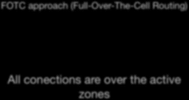
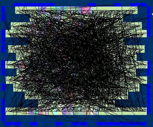
22 Connections becomes the central problem! Challenge: how to reduce wirelength?
23 Challenge: how to reduce wirelength? - area reduction - use of complex gates (SCCG) - improvement of routing and placement algorithms


24 Using Static CMOS Complex Gates (SCCG) with cell generation on-the-fly It is possible do to an extreme logic minimization Freedom to Logic Designers!!!!
) A B S C D 14 Transistors")
25 Example A B C D S S = A + ( B + (C+D)) A B S C D 14 Transistors
26 Use of SCCG S = A + ( B + (C+D)) S = A + ( B.(C+D)) B D C A A S B C S A D D B C 8 Transistors
27 Use of SCCG S = A + ( B + (C+D)) S = A + ( B.(C+D)) A A B C D S B C D S 14 Transistors 8 Transistors

28 Automatic Layout Synthesis Using Complex Gates (SCCG) NUMBER OF SERIAL NMOS TRANSISTORS NUMBER OF SERIAL PMOS TRANSISTORS


29 ower eduction I leakage is become important in submicron circuits. It is function of the number of transistors

30 Routing the solutions produced by academic and industrial tools are in average within 1.43 to 2.38 times the optimal solutions considering wirelength C-C. Chang, J. Cong, M. Xie. Optimality and Scalability of Existing Placement Algorithms. ASPDAC 2003


31 FOTC Routing FOTC approach (Full-Over-The-Cell Routing) All conections are over the active zones

32 ayout trategies

33 Layout Strategies - transistor topologies - management of routing in all layers - VCC and Ground distribution - clock distribution - contacts and vias management - body ties management - transistor sizing and folding


34 Layout Strategies Transistor topologies - horizontal - vertical - doglegs (different directions) - folding

35 Transistor Folding 35
36 Transistor Folding 36

37 Layout Strategies Routing Management - priority tracks schema - routing layers priority - routing layers directions
 - over the transistors Layer (metal 1, metal 2,.")
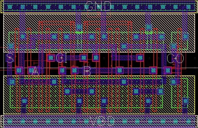
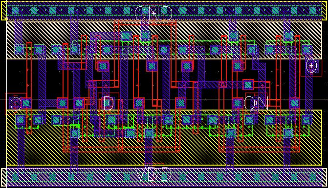
38 Layout Strategies VCC and Ground Distribution - borders of the strip - middle of strips (between P and N diffusions) - over the transistors Layer (metal 1, metal 2,...)

39 Power Lines over the transistors TROPIC3
 gnd (metal2) N diffusion Over-the-cell")
40 Power Lines between P and N plans Optimized Jog in polysilicon wire Aligned pins with jog in polysilicon. Transistor not aligned Not aligned pin P diffusion Connetion between N and P plan in metal1 vcc (metal2) gnd (metal2) N diffusion Over-the-cell routing Metal1 to connect supply line TROPIC3

41 Power Lines at the Strip Borders Parrot1

42 Layout Strategies - contacts and vias management - body ties management

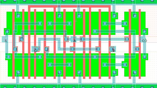
43 Layout Strategies contacts and vias management (towers of vias)
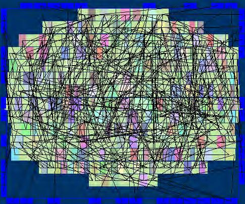
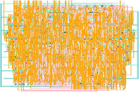
44 Compaction Results Summary: 8150 Variables Constraints runtime: 20 segs Weights: Diffusion 3 Poly 3 Metal 1 Transistor-Level Automatic Layout Generation of Radiation-Hardened Circuits
45 Compaction Results Poly lines Reduction Transistor-Level Automatic Layout Generation of Radiation-Hardened Circuits
46 Compaction Results Metal lines Reduction Transistor-Level Automatic Layout Generation of Radiation-Hardened Circuits
47 Compaction Results Diffusion Reduction Transistor-Level Automatic Layout Generation of Radiation-Hardened Circuits

48 Physical Design Flow


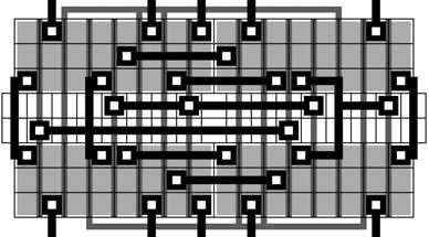
49 Logic Netlist Partitioning and Placement Routing Cell Generation Automatic Characterization Timing Power Circuit Layout
50 Layout Generation Flow Circuit Placement Specifications Design Rules Transistor Placement Layout Generation Routing Layout 50

51 Wirelength Placement with wirelength reduction
52


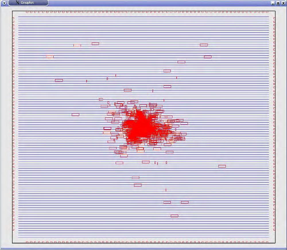
53 Congestion Congestion is an important problem because it can forbid a complete routing Routability


54 Compromise: Routability and Wirelength Reduction

55 Parrot Layout Style

56 Layout Generated Automatically with Parrot Tool Suite


57 432 TROPIC PARROT 804 transistors Delay: % Area: %


58 499 TROPIC PARROT 1556 transistors Delay: % Area: %


59 880 TROPIC PARROT 1802 transistors Delay: % Area: %


60 1355 TROPIC PARROT 2308 transistors Delay: % Area: %

61 Results: Layouts

62 Results: Layouts --- ( transistors JK1 (34 62
63 ADD32

64 Adder Adder Mux Register

65 Results: Layouts Non-Complementary Logic ( transistors LBBDD_ F177F7FFF (68 Runtime: 36 min L.S.da Rosa Jr., F.Marques, T.M.G.Cardoso, R.P.Ribas, S.S.Sapatnekar, A.I.Reis, Fast Transistor Networks from BDDs. SBCCI 2006, pp

66 Data Path Design Automation
67 Multiplier Carry-Save 4x4 Standard Cell (Cadence Flow) Generated with our Data Path Compiler
68 Multiplier Carry-Save 4x4 Standard Cell Cell Compiler Gain (%) Number of Cells Number of Transistors Area (µm 2 ) Delay (ps) Power (mw)
69 Conclusions

70 Conclusions Cell generated on-the-fly target to their environment Area reduction Reduction on the number of transistors Cell library free Wirelength minimization Power Reduction Delay Reduction

71 Conclusions Let s do Transistor Level Design Automation
72 Electronic Design Automation at Transistor Level Ricardo Reis Universidade Federal do Rio Grande do Sul Instituto de Informática - Porto Alegre - RS - Brasil reis@inf.ufrgs.br
Low Power 3-2 and 4-2 Adder Compressors Implemented Using ASTRAN
 XXVII SIM - South Symposium on Microelectronics 1 Low Power 3-2 and 4-2 Adder Compressors Implemented Using ASTRAN Jorge Tonfat, Ricardo Reis jorgetonfat@ieee.org, reis@inf.ufrgs.br Grupo de Microeletrônica
Disseny físic. Disseny en Standard Cells. Enric Pastor Rosa M. Badia Ramon Canal DM Tardor DM, Tardor
 Disseny físic Disseny en Standard Cells Enric Pastor Rosa M. Badia Ramon Canal DM Tardor 2005 DM, Tardor 2005 1 Design domains (Gajski) Structural Processor, memory ALU, registers Cell Device, gate Transistor
Transistor Network Restructuring Against NBTI Degradation. P. F. Butzen a, V. Dal Bem a, A. I. Reis b, R. P. Ribas b.
 Transistor Network Restructuring Against NBTI Degradation. P. F. Butzen a, V. Dal Bem a, A. I. Reis b, R. P. Ribas b. a PGMICRO, Federal University of Rio Grande do Sul, Porto Alegre, Brazil b Institute
EE 434 ASIC and Digital Systems. Prof. Dae Hyun Kim School of Electrical Engineering and Computer Science Washington State University.
 EE 434 ASIC and Digital Systems Prof. Dae Hyun Kim School of Electrical Engineering and Computer Science Washington State University Preliminaries VLSI Design System Specification Functional Design RTL
CHAPTER 3 NEW SLEEPY- PASS GATE
 56 CHAPTER 3 NEW SLEEPY- PASS GATE 3.1 INTRODUCTION A circuit level design technique is presented in this chapter to reduce the overall leakage power in conventional CMOS cells. The new leakage po leepy-
Learning Outcomes. Spiral 2 8. Digital Design Overview LAYOUT
 2-8.1 2-8.2 Spiral 2 8 Cell Mark Redekopp earning Outcomes I understand how a digital circuit is composed of layers of materials forming transistors and wires I understand how each layer is expressed as
Low Power VLSI Circuit Synthesis: Introduction and Course Outline
 Low Power VLSI Circuit Synthesis: Introduction and Course Outline Ajit Pal Professor Department of Computer Science and Engineering Indian Institute of Technology Kharagpur INDIA -721302 Agenda Why Low
Very Large Scale Integration (VLSI)
") Very Large Scale Integration (VLSI) Lecture 6 Dr. Ahmed H. Madian Ah_madian@hotmail.com Dr. Ahmed H. Madian-VLSI 1 Contents Array subsystems Gate arrays technology Sea-of-gates Standard cell Macrocell
Very Large Scale Integration (VLSI) Lecture 6 Dr. Ahmed H. Madian Ah_madian@hotmail.com Dr. Ahmed H. Madian-VLSI 1 Contents Array subsystems Gate arrays technology Sea-of-gates Standard cell Macrocell
Jack Keil Wolf Lecture. ESE 570: Digital Integrated Circuits and VLSI Fundamentals. Lecture Outline. MOSFET N-Type, P-Type.
 ESE 570: Digital Integrated Circuits and VLSI Fundamentals Jack Keil Wolf Lecture Lec 3: January 24, 2019 MOS Fabrication pt. 2: Design Rules and Layout http://www.ese.upenn.edu/about-ese/events/wolf.php
ESE 570: Digital Integrated Circuits and VLSI Fundamentals
 ESE 570: Digital Integrated Circuits and VLSI Fundamentals Lec 3: January 24, 2019 MOS Fabrication pt. 2: Design Rules and Layout Penn ESE 570 Spring 2019 Khanna Jack Keil Wolf Lecture http://www.ese.upenn.edu/about-ese/events/wolf.php
An Efficient Layout Style for Three Metal CMOS Macro-Cells
 34 An Efficient Layout Style for Three Metal CMOS Macro-Cells F. Moraes PUC-RS- Av. Ipiranga, 668 CEP 90619-900, Porto Alegre, Brazil Phone: +55(0)513391511, FAX: +55(0)513391564 e-mail: moraes@ andros.pucrs.
! Review: MOS IV Curves and Switch Model. ! MOS Device Layout. ! Inverter Layout. ! Gate Layout and Stick Diagrams. ! Design Rules. !
 ESE 570: Digital Integrated Circuits and VLSI Fundamentals Lec 3: January 21, 2017 MOS Fabrication pt. 2: Design Rules and Layout Lecture Outline! Review: MOS IV Curves and Switch Model! MOS Device Layout!
Enhancement of Design Quality for an 8-bit ALU
 ABHIYANTRIKI An International Journal of Engineering & Technology (A Peer Reviewed & Indexed Journal) Vol. 3, No. 5 (May, 2016) http://www.aijet.in/ eissn: 2394-627X Enhancement of Design Quality for an
18nm FinFET. Lecture 30. Perspectives. Administrivia. Power Density. Power will be a problem. Transistor Count
 18nm FinFET Double-gate structure + raised source/drain Lecture 30 Perspectives Gate Silicon Fin Source BOX Gate X. Huang, et al, 1999 IEDM, p.67~70 Drain Si fin - Body! I d [ua/um] 400-1.50 V 350 300-1.25
TEACHING UNDERGRADUATES TO DESIGN WITH VHDL
 TEACHING UNDERGRADUATES TO DESIGN WITH VHDL Edval J. P. Santos, Altamiro A. Suzim(*), Alberto C. Mesquita Jr., Departamento de Eletrônica e Sistemas, Universidade Federal de Pernambuco Recife-PE, Brazil
ALPS: An Automatic Layouter for Pass-Transistor Cell Synthesis
 ALPS: An Automatic Layouter for Pass-Transistor Cell Synthesis Yasuhiko Sasaki Central Research Laboratory Hitachi, Ltd. Kokubunji, Tokyo, 185, Japan Kunihito Rikino Hitachi Device Engineering Kokubunji,
Lecture Perspectives. Administrivia
 Lecture 29-30 Perspectives Administrivia Final on Friday May 18 12:30-3:30 pm» Location: 251 Hearst Gym Topics all what was covered in class. Review Session Time and Location TBA Lab and hw scores to be
Power-Delivery Network in 3D ICs: Monolithic 3D vs. Skybridge 3D CMOS
 -Delivery Network in 3D ICs: Monolithic 3D vs. Skybridge 3D CMOS Jiajun Shi, Mingyu Li and Csaba Andras Moritz Department of Electrical and Computer Engineering University of Massachusetts, Amherst, MA,
Course Outcome of M.Tech (VLSI Design)
") Course Outcome of M.Tech (VLSI Design) PVL108: Device Physics and Technology The students are able to: 1. Understand the basic physics of semiconductor devices and the basics theory of PN junction. 2.
Course Outcome of M.Tech (VLSI Design) PVL108: Device Physics and Technology The students are able to: 1. Understand the basic physics of semiconductor devices and the basics theory of PN junction. 2.
Technology Timeline. Transistors ICs (General) SRAMs & DRAMs Microprocessors SPLDs CPLDs ASICs. FPGAs. The Design Warrior s Guide to.
 SRAMs & DRAMs Microprocessors SPLDs CPLDs ASICs. FPGAs. The Design Warrior s Guide to.") FPGAs 1 CMPE 415 Technology Timeline 1945 1950 1955 1960 1965 1970 1975 1980 1985 1990 1995 2000 Transistors ICs (General) SRAMs & DRAMs Microprocessors SPLDs CPLDs ASICs FPGAs The Design Warrior s Guide
FPGAs 1 CMPE 415 Technology Timeline 1945 1950 1955 1960 1965 1970 1975 1980 1985 1990 1995 2000 Transistors ICs (General) SRAMs & DRAMs Microprocessors SPLDs CPLDs ASICs FPGAs The Design Warrior s Guide
Lecture 30. Perspectives. Digital Integrated Circuits Perspectives
 Lecture 30 Perspectives Administrivia Final on Friday December 15 8 am Location: 251 Hearst Gym Topics all what was covered in class. Precise reading information will be posted on the web-site Review Session
CMOS VLSI IC Design. A decent understanding of all tasks required to design and fabricate a chip takes years of experience
 CMOS VLSI IC Design A decent understanding of all tasks required to design and fabricate a chip takes years of experience 1 Commonly used keywords INTEGRATED CIRCUIT (IC) many transistors on one chip VERY
LSI Design Flow Development for Advanced Technology
 LSI Design Flow Development for Advanced Technology Atsushi Tsuchiya LSIs that adopt advanced technologies, as represented by imaging LSIs, now contain 30 million or more logic gates and the scale is beginning
Digital Integrated Circuits Perspectives. Administrivia
 Lecture 30 Perspectives Administrivia Final on Friday December 14, 2001 8 am Location: 180 Tan Hall Topics all what was covered in class. Review Session - TBA Lab and hw scores to be posted on the web
! Review: MOS IV Curves and Switch Model. ! MOS Device Layout. ! Inverter Layout. ! Gate Layout and Stick Diagrams. ! Design Rules. !
 ESE 570: Digital Integrated Circuits and VLSI Fundamentals Lec 3: January 21, 2016 MOS Fabrication pt. 2: Design Rules and Layout Lecture Outline! Review: MOS IV Curves and Switch Model! MOS Device Layout!
ESE 570: Digital Integrated Circuits and VLSI Fundamentals
 ESE 570: Digital Integrated Circuits and VLSI Fundamentals Lec 3: January 21, 2016 MOS Fabrication pt. 2: Design Rules and Layout Penn ESE 570 Spring 2016 Khanna Adapted from GATech ESE3060 Slides Lecture
Low Power Design Part I Introduction and VHDL design. Ricardo Santos LSCAD/FACOM/UFMS
 Low Power Design Part I Introduction and VHDL design Ricardo Santos ricardo@facom.ufms.br LSCAD/FACOM/UFMS Motivation for Low Power Design Low power design is important from three different reasons Device
AN EFFICIENT APPROACH TO MINIMIZE POWER AND AREA IN CARRY SELECT ADDER USING BINARY TO EXCESS ONE CONVERTER
 AN EFFICIENT APPROACH TO MINIMIZE POWER AND AREA IN CARRY SELECT ADDER USING BINARY TO EXCESS ONE CONVERTER K. RAMAMOORTHY 1 T. CHELLADURAI 2 V. MANIKANDAN 3 1 Department of Electronics and Communication
Layout - Line of Diffusion. Where are we? Line of Diffusion in General. Line of Diffusion in General. Stick Diagrams. Line of Diffusion in General
 Where are we? Lots of Layout issues Line of diffusion style Power pitch it-slice pitch Routing strategies Transistor sizing Wire sizing Layout - Line of Diffusion Very common layout method Start with a
IT IS BELIEVED that in today s logic designs, interconnects
 1892 IEEE TRANSACTIONS ON COMPUTER-AIDED DESIGN OF INTEGRATED CIRCUITS AND SYSTEMS, VOL. 32, NO. 12, DECEMBER 2013 Ultrahigh Density Logic Designs Using Monolithic 3-D Integration Young-Joon Lee, Student
Design Methodologies. Digital Integrated Circuits A Design Perspective. Jan M. Rabaey Anantha Chandrakasan Borivoje Nikolic.
 Digital Integrated Circuits A Design Perspective Jan M. Rabaey Anantha Chandrakasan Borivoje Nikolic Design Methodologies December 10, 2002 L o g i c T r a n s i s t o r s p e r C h i p ( K ) 1 9 8 1 1
Microelectronics, BSc course
 Microelectronics, BSc course MOS circuits: CMOS circuits, construction http://www.eet.bme.hu/~poppe/miel/en/14-cmos.pptx http://www.eet.bme.hu The abstraction level of our study: SYSTEM + MODULE GATE CIRCUIT
Design Methodologies. Digital Integrated Circuits A Design Perspective. Jan M. Rabaey Anantha Chandrakasan Borivoje Nikolic.
 Digital Integrated Circuits A Design Perspective Jan M. Rabaey Anantha Chandrakasan Borivoje Nikolic Design Methodologies December 10, 2002 L o g i c T r a n s i s t o r s p e r C h i p ( K ) 1 9 8 1 1
Novel Low-Overhead Operand Isolation Techniques for Low-Power Datapath Synthesis
 Novel Low-Overhead Operand Isolation Techniques for Low-Power Datapath Synthesis N. Banerjee, A. Raychowdhury, S. Bhunia, H. Mahmoodi, and K. Roy School of Electrical and Computer Engineering, Purdue University,
Tiago Reimann Cliff Sze Ricardo Reis. Gate Sizing and Threshold Voltage Assignment for High Performance Microprocessor Designs
 Tiago Reimann Cliff Sze Ricardo Reis Gate Sizing and Threshold Voltage Assignment for High Performance Microprocessor Designs A grain of rice has the price of more than a 100 thousand transistors Source:
Power Benefit Study for Ultra-High Density Transistor-Level Monolithic 3D ICs
 Power Benefit Study for Ultra-High Density Transistor-Level Monolithic 3D ICs ABSTRACT The nano-scale 3D interconnects available in monolithic 3D IC technology enable ultra-high density device integration
Design and Implementation of Complex Multiplier Using Compressors
 Design and Implementation of Complex Multiplier Using Compressors Abstract: In this paper, a low-power high speed Complex Multiplier using compressor circuit is proposed for fast digital arithmetic integrated
PERFORMANCE COMPARISON OF DIGITAL GATES USING CMOS AND PASS TRANSISTOR LOGIC USING CADENCE VIRTUOSO
 PERFORMANCE COMPARISON OF DIGITAL GATES USING CMOS AND PASS TRANSISTOR LOGIC USING CADENCE VIRTUOSO Paras Gupta 1, Pranjal Ahluwalia 2, Kanishk Sanwal 3, Peyush Pande 4 1,2,3,4 Department of Electronics
Mixed Signal Virtual Components COLINE, a case study
 Mixed Signal Virtual Components COLINE, a case study J.F. POLLET - DOLPHIN INTEGRATION Meylan - FRANCE http://www.dolphin.fr Overview of the presentation Introduction COLINE, an example of Mixed Signal
CHAPTER 3 PERFORMANCE OF A TWO INPUT NAND GATE USING SUBTHRESHOLD LEAKAGE CONTROL TECHNIQUES
 CHAPTER 3 PERFORMANCE OF A TWO INPUT NAND GATE USING SUBTHRESHOLD LEAKAGE CONTROL TECHNIQUES 41 In this chapter, performance characteristics of a two input NAND gate using existing subthreshold leakage
A Case Study of Nanoscale FPGA Programmable Switches with Low Power
 A Case Study of Nanoscale FPGA Programmable Switches with Low Power V.Elamaran 1, Har Narayan Upadhyay 2 1 Assistant Professor, Department of ECE, School of EEE SASTRA University, Tamilnadu - 613401, India
I/O Design EE141. Announcements. EE141-Fall 2006 Digital Integrated Circuits. Class Material. Pads + ESD Protection.
 EE141-Fall 2006 Digital Integrated Circuits nnouncements Homework 9 due on Thursday Lecture 26 I/O 1 2 Class Material Last lecture Timing Clock distribution Today s lecture I/O Power distribution Intro
Digital Systems Design
 Digital Systems Design Digital Systems Design and Test Dr. D. J. Jackson Lecture 1-1 Introduction Traditional digital design Manual process of designing and capturing circuits Schematic entry System-level
EE 434 ASIC & Digital Systems
 EE 434 ASIC & Digital Systems Dae Hyun Kim EECS Washington State University Spring 2017 Course Website http://eecs.wsu.edu/~ee434 Themes Study how to design, analyze, and test a complex applicationspecific
Homework 10 posted just for practice. Office hours next week, schedule TBD. HKN review today. Your feedback is important!
 EE141 Fall 2005 Lecture 26 Memory (Cont.) Perspectives Administrative Stuff Homework 10 posted just for practice No need to turn in Office hours next week, schedule TBD. HKN review today. Your feedback
Chapter 3 Chip Planning
 Chapter 3 Chip Planning 3.1 Introduction to Floorplanning 3. Optimization Goals in Floorplanning 3.3 Terminology 3.4 Floorplan Representations 3.4.1 Floorplan to a Constraint-Graph Pair 3.4. Floorplan
Lecture 0: Introduction
 Lecture 0: Introduction Introduction Integrated circuits: many transistors on one chip. Very Large Scale Integration (VLSI): bucketloads! Complementary Metal Oxide Semiconductor Fast, cheap, low power
Interconnect-Power Dissipation in a Microprocessor
 4/2/2004 Interconnect-Power Dissipation in a Microprocessor N. Magen, A. Kolodny, U. Weiser, N. Shamir Intel corporation Technion - Israel Institute of Technology 4/2/2004 2 Interconnect-Power Definition
An Implementation of a 32-bit ARM Processor Using Dual Power Supplies and Dual Threshold Voltages
 An Implementation of a 32-bit ARM Processor Using Dual Supplies and Dual Threshold Voltages Robert Bai, Sarvesh Kulkarni, Wesley Kwong, Ashish Srivastava, Dennis Sylvester, David Blaauw University of Michigan,
Sticks Diagram & Layout. Part II
 Sticks Diagram & Layout Part II Well and Substrate Taps Substrate must be tied to GND and n-well to V DD Metal to lightly-doped semiconductor forms poor connection called Shottky Diode Use heavily doped
Lecture 9: Cell Design Issues
 Lecture 9: Cell Design Issues MAH, AEN EE271 Lecture 9 1 Overview Reading W&E 6.3 to 6.3.6 - FPGA, Gate Array, and Std Cell design W&E 5.3 - Cell design Introduction This lecture will look at some of the
EE141-Spring 2007 Digital Integrated Circuits
 EE141-Spring 2007 Digital Integrated Circuits Lecture 22 I/O, Power Distribution dders 1 nnouncements Homework 9 has been posted Due Tu. pr. 24, 5pm Project Phase 4 (Final) Report due Mo. pr. 30, noon
+1 (479)
") Introduction to VLSI Design http://csce.uark.edu +1 (479) 575-6043 yrpeng@uark.edu Invention of the Transistor Vacuum tubes ruled in first half of 20th century Large, expensive, power-hungry, unreliable
Introduction to VLSI Design http://csce.uark.edu +1 (479) 575-6043 yrpeng@uark.edu Invention of the Transistor Vacuum tubes ruled in first half of 20th century Large, expensive, power-hungry, unreliable
2009 Spring CS211 Digital Systems & Lab 1 CHAPTER 3: TECHNOLOGY (PART 2)
") 1 CHAPTER 3: IMPLEMENTATION TECHNOLOGY (PART 2) Whatwillwelearninthischapter? we learn in this 2 How transistors operate and form simple switches CMOS logic gates IC technology FPGAs and other PLDs Basic
1 CHAPTER 3: IMPLEMENTATION TECHNOLOGY (PART 2) Whatwillwelearninthischapter? we learn in this 2 How transistors operate and form simple switches CMOS logic gates IC technology FPGAs and other PLDs Basic
Low-Power Digital CMOS Design: A Survey
 Low-Power Digital CMOS Design: A Survey Krister Landernäs June 4, 2005 Department of Computer Science and Electronics, Mälardalen University Abstract The aim of this document is to provide the reader with
! MOS Device Layout. ! Inverter Layout. ! Gate Layout and Stick Diagrams. ! Design Rules. ! Standard Cells. ! CMOS Process Enhancements
 EE 570: igital Integrated Circuits and VLI Fundamentals Lec 3: January 18, 2018 MO Fabrication pt. 2: esign Rules and Layout Lecture Outline! MO evice Layout! Inverter Layout! Gate Layout and tick iagrams!
EDA Challenges for Low Power Design. Anand Iyer, Cadence Design Systems
 EDA Challenges for Low Power Design Anand Iyer, Cadence Design Systems Agenda Introduction ti LP techniques in detail Challenges to low power techniques Guidelines for choosing various techniques Why is
CS250 VLSI Systems Design. Lecture 3: Physical Realities: Beneath the Digital Abstraction, Part 1: Timing
 CS250 VLSI Systems Design Lecture 3: Physical Realities: Beneath the Digital Abstraction, Part 1: Timing Fall 2010 Krste Asanovic, John Wawrzynek with John Lazzaro and Yunsup Lee (TA) What do Computer
MHz phase-locked loop
 SPECIFICATION 1 FEATURES 50 800 MHz phase-locked loop TSMC CMOS 65 nm Output frequency from 50 to 800 MHz Reference frequency from 4 to 30 MHz Power supply 1.2 V CMOS output Supported foundries: TSMC,
Gdi Technique Based Carry Look Ahead Adder Design
 IOSR Journal of VLSI and Signal Processing (IOSR-JVSP) Volume 4, Issue 6, Ver. I (Nov - Dec. 2014), PP 01-09 e-issn: 2319 4200, p-issn No. : 2319 4197 Gdi Technique Based Carry Look Ahead Adder Design
Digital Integrated Circuits 1: Fundamentals
 Digital Integrated Circuits 1: Fundamentals Atsushi Takahashi Department of Information and Communications Engineering School of Engineering Tokyo Institute of Technology 1 VLSI and Computer System VLSI
CPE/EE 427, CPE 527 VLSI Design I: Homeworks 3 & 4
 CPE/EE 427, CPE 527 VLSI Design I: Homeworks 3 & 4 1 2 3 4 5 6 7 8 9 10 Sum 30 10 25 10 30 40 10 15 15 15 200 1. (30 points) Misc, Short questions (a) (2 points) Postponing the introduction of signals
Design Rules, Technology File, DRC / LVS
 Design Rules, Technology File, DRC / LVS Prof. Dr. Peter Fischer VLSI Design: Design Rules P. Fischer, TI, Uni Mannheim, Seite 1 DESIGN RULES Rules in one Layer Caused by manufacturing limits (lithography,
Low Power Design Methods: Design Flows and Kits
 JOINT ADVANCED STUDENT SCHOOL 2011, Moscow Low Power Design Methods: Design Flows and Kits Reported by Shushanik Karapetyan Synopsys Armenia Educational Department State Engineering University of Armenia
A NOVEL 4-Bit ARITHMETIC LOGIC UNIT DESIGN FOR POWER AND AREA OPTIMIZATION
 A NOVEL 4-Bit ARITHMETIC LOGIC UNIT DESIGN FOR POWER AND AREA OPTIMIZATION Mr. Snehal Kumbhalkar 1, Mr. Sanjay Tembhurne 2 Department of Electronics and Communication Engineering GHRAET, Nagpur, Maharashtra,
CS 6135 VLSI Physical Design Automation Fall 2003
 CS 6135 VLSI Physical Design Automation Fall 2003 1 Course Information Class time: R789 Location: EECS 224 Instructor: Ting-Chi Wang ( ) EECS 643, (03) 5742963 tcwang@cs.nthu.edu.tw Office hours: M56R5
Low Power Radiation Tolerant CMOS Design using Commercial Fabrication Processes
 Low Power Radiation Tolerant CMOS Design using Commercial Fabrication Processes Amir Hasanbegovic (amirh@ifi.uio.no) Nanoelectronics Group, Dept. of Informatics, University of Oslo November 5, 2010 Overview
Towards PVT-Tolerant Glitch-Free Operation in FPGAs
 Towards PVT-Tolerant Glitch-Free Operation in FPGAs Safeen Huda and Jason H. Anderson ECE Department, University of Toronto, Canada 24 th ACM/SIGDA International Symposium on FPGAs February 22, 2016 Motivation
Design and Implementation of an Ultra-Low Power High Speed CMOS Logic using Cadence
 Design and Implementation of an Ultra-Low Power High Speed CMOS Logic using Cadence L.Vasanth 1, D. Yokeshwari 2 1 Assistant Professor, 2 PG Scholar, Department of ECE Tejaa Shakthi Institute of Technology
Hot Topics and Cool Ideas in Scaled CMOS Analog Design
 Engineering Insights 2006 Hot Topics and Cool Ideas in Scaled CMOS Analog Design C. Patrick Yue ECE, UCSB October 27, 2006 Slide 1 Our Research Focus High-speed analog and RF circuits Device modeling,
Low Power, Area Efficient FinFET Circuit Design
 Low Power, Area Efficient FinFET Circuit Design Michael C. Wang, Princeton University Abstract FinFET, which is a double-gate field effect transistor (DGFET), is more versatile than traditional single-gate
Announcements. Advanced Digital Integrated Circuits. Quiz #3 today Homework #4 posted This lecture until 4pm
 EE241 - Spring 2011 dvanced Digital Integrated Circuits Lecture 20: High-Performance Logic Styles nnouncements Quiz #3 today Homework #4 posted This lecture until 4pm Reading: Chapter 8 in the owhill text
Introduction to CMOS VLSI Design (E158) Lecture 9: Cell Design
 Lecture 9: Cell Design") Harris Introduction to CMOS VLSI Design (E158) Lecture 9: Cell Design David Harris Harvey Mudd College David_Harris@hmc.edu Based on EE271 developed by Mark Horowitz, Stanford University MAH E158 Lecture
Harris Introduction to CMOS VLSI Design (E158) Lecture 9: Cell Design David Harris Harvey Mudd College David_Harris@hmc.edu Based on EE271 developed by Mark Horowitz, Stanford University MAH E158 Lecture
Development of a Radiation Tolerant 2.0 V standard cell library using a commercial deep submicron CMOS technology for the LHC experiments.
 Development of a Radiation Tolerant 2.0 V standard cell library using a commercial deep submicron CMOS technology for the LHC experiments. K. Kloukinas, F. Faccio, A. Marchioro, P. Moreira, CERN/EP-MIC,
Leakage Power Minimization in Deep-Submicron CMOS circuits
 Outline Leakage Power Minimization in Deep-Submicron circuits Politecnico di Torino Dip. di Automatica e Informatica 1019 Torino, Italy enrico.macii@polito.it Introduction. Design for low leakage: Basics.
Design and Analysis of Low Power 2-bit and 4-bit Digital Comparators in 45nm and 90nm CMOS Technologies
 International Journal of Engineering and Technical Research (IJETR) Design and Analysis of Low Power 2-bit and 4-bit Digital Comparators in 45nm and 90nm CMOS Technologies Agrakshi, Suman Rani Abstract
A Novel Low-Power Scan Design Technique Using Supply Gating
 A Novel Low-Power Scan Design Technique Using Supply Gating S. Bhunia, H. Mahmoodi, S. Mukhopadhyay, D. Ghosh, and K. Roy School of Electrical and Computer Engineering, Purdue University, West Lafayette,
Introduction to Electronic Design Automation
 Introduction to Electronic Design Automation Jie-Hong Roland Jiang 江介宏 Department of Electrical Engineering National Taiwan University Spring 2014 1 Design Automation? 2 Course Info (1/4) Instructor Jie-Hong
High Performance Low-Power Signed Multiplier
 High Performance Low-Power Signed Multiplier Amir R. Attarha Mehrdad Nourani VLSI Circuits & Systems Laboratory Department of Electrical and Computer Engineering University of Tehran, IRAN Email: attarha@khorshid.ece.ut.ac.ir
Digital Signal Processing for an Integrated Power-Meter
 49. Internationales Wissenschaftliches Kolloquium Technische Universität Ilmenau 27.-30. September 2004 Borisav Jovanović / Milunka Damnjanović / Predrag Petković Digital Signal Processing for an Integrated
A 0.9 V Low-power 16-bit DSP Based on a Top-down Design Methodology
 UDC 621.3.049.771.14:621.396.949 A 0.9 V Low-power 16-bit DSP Based on a Top-down Design Methodology VAtsushi Tsuchiya VTetsuyoshi Shiota VShoichiro Kawashima (Manuscript received December 8, 1999) A 0.9
Comparison of Multiplier Design with Various Full Adders
 Comparison of Multiplier Design with Various Full s Aruna Devi S 1, Akshaya V 2, Elamathi K 3 1,2,3Assistant Professor, Dept. of Electronics and Communication Engineering, College, Tamil Nadu, India ---------------------------------------------------------------------***----------------------------------------------------------------------
Introduction to deep-submicron CMOS circuit design
 National Institute of Applied Sciences Department of Electrical & Computer Engineering Introduction to deep-submicron CMOS circuit design Etienne Sicard http:\\intrage.insa-tlse.fr\~etienne 1 08/09/00
CMOS Digital Logic Design with Verilog. Chapter1 Digital IC Design &Technology
 CMOS Digital Logic Design with Verilog Chapter1 Digital IC Design &Technology Chapter Overview: In this chapter we study the concept of digital hardware design & technology. This chapter deals the standard
420 Intro to VLSI Design
 Dept of Electrical and Computer Engineering 420 Intro to VLSI Design Lecture 0: Course Introduction and Overview Valencia M. Joyner Spring 2005 Getting Started Syllabus About the Instructor Labs, Problem
28nm and below: New Frontiers and Innovations in Design for Manufacturing. Vito Dai, Ph.D. Sr. Member of Technical Staff, DFM
 28nm and below: New Frontiers and Innovations in Design for Manufacturing Vito Dai, Ph.D. Sr. Member of Technical Staff, DFM Outline Challenges Variability and the Limits of IC Geometrical Scaling Methodology
Jan Rabaey, «Low Powere Design Essentials," Springer tml
 Jan Rabaey, «e Design Essentials," Springer 2009 http://web.me.com/janrabaey/lowpoweressentials/home.h tml Dimitrios Soudris, Christian Piguet, and Costas Goutis, Designing CMOS Circuits for Low POwer,
Design of High-Performance Intra Prediction Circuit for H.264 Video Decoder
 JOURNAL OF SEMICONDUCTOR TECHNOLOGY AND SCIENCE, VOL.9, NO.4, DECEMBER, 2009 187 Design of High-Performance Intra Prediction Circuit for H.264 Video Decoder Jihye Yoo, Seonyoung Lee, and Kyeongsoon Cho
Lecture 1. Tinoosh Mohsenin
 Lecture 1 Tinoosh Mohsenin Today Administrative items Syllabus and course overview Digital systems and optimization overview 2 Course Communication Email Urgent announcements Web page http://www.csee.umbc.edu/~tinoosh/cmpe650/
INTERNATIONAL JOURNAL OF PURE AND APPLIED RESEARCH IN ENGINEERING AND TECHNOLOGY
 INTERNATIONAL JOURNAL OF PURE AND APPLIED RESEARCH IN ENGINEERING AND TECHNOLOGY A PATH FOR HORIZING YOUR INNOVATIVE WORK QUATERNARY ARITHMETIC LOGIC UNIT BASED ON QSD TECHNIQUE PRAJAKTA V. DESHMUKH, MUKESH
MS Project :Trading Accuracy for Power with an Under-designed Multiplier Architecture Parag Kulkarni Adviser : Prof. Puneet Gupta Electrical Eng.
 MS Project :Trading Accuracy for Power with an Under-designed Multiplier Architecture Parag Kulkarni Adviser : Prof. Puneet Gupta Electrical Eng., UCLA - http://nanocad.ee.ucla.edu/ 1 Outline Introduction
Introduction to CMOS VLSI Design (E158) Lecture 5: Logic
 Lecture 5: Logic") Harris Introduction to CMOS VLSI Design (E158) Lecture 5: Logic David Harris Harvey Mudd College David_Harris@hmc.edu Based on EE271 developed by Mark Horowitz, Stanford University MAH E158 Lecture 5 1
Harris Introduction to CMOS VLSI Design (E158) Lecture 5: Logic David Harris Harvey Mudd College David_Harris@hmc.edu Based on EE271 developed by Mark Horowitz, Stanford University MAH E158 Lecture 5 1
A Low-Power High-speed Pipelined Accumulator Design Using CMOS Logic for DSP Applications
 International Journal of Research Studies in Computer Science and Engineering (IJRSCSE) Volume. 1, Issue 5, September 2014, PP 30-42 ISSN 2349-4840 (Print) & ISSN 2349-4859 (Online) www.arcjournals.org
Mapping Multiplexers onto Hard Multipliers in FPGAs
 Mapping Multiplexers onto Hard Multipliers in FPGAs Peter Jamieson and Jonathan Rose The Edward S. Rogers Sr. Department of Electrical and Computer Engineering University of Toronto Modern FPGAs Consist
Noise Constraint Driven Placement for Mixed Signal Designs. William Kao and Wenkung Chu October 20, 2003 CAS IEEE SCV Meeting
 Noise Constraint Driven Placement for Mixed Signal Designs William Kao and Wenkung Chu October 20, 2003 CAS IEEE SCV Meeting Introduction OUTLINE Substrate Noise: Some Background Substrate Noise Network
DESIGN FOR LOW-POWER USING MULTI-PHASE AND MULTI- FREQUENCY CLOCKING
 3 rd Int. Conf. CiiT, Molika, Dec.12-15, 2002 31 DESIGN FOR LOW-POWER USING MULTI-PHASE AND MULTI- FREQUENCY CLOCKING M. Stojčev, G. Jovanović Faculty of Electronic Engineering, University of Niš Beogradska
2 Assoc Prof, Dept of ECE, George Institute of Engineering & Technology, Markapur, AP, India,
 ISSN 2319-8885 Vol.03,Issue.30 October-2014, Pages:5968-5972 www.ijsetr.com Low Power and Area-Efficient Carry Select Adder THANNEERU DHURGARAO 1, P.PRASANNA MURALI KRISHNA 2 1 PG Scholar, Dept of DECS,
Routability in 3D IC Design: Monolithic 3D vs. Skybridge 3D CMOS
 Routability in 3D IC Design: Monolithic 3D vs. Skybridge 3D CMOS Jiajun Shi 1, Mingyu Li 1, Santosh Khasanvis 3, Mostafizur Rahman 2 and Csaba Andras Moritz 1 1 Department of Electrical and Computer Engineering,
DESIGN AND IMPLEMENTATION OF A STANDARD CELL LIBRARY FOR BUILDING ASYNCHRONOUS ASICS
 PONTIFÍCIA UNIVERSIDADE CATÓLICA DO RIO GRANDE DO SUL FACULDADE DE ENGENHARIA FACULDADE DE INFORMÁTICA ENGENHARIA DE COMPUTAÇÃO DESIGN AND IMPLEMENTATION OF A STANDARD CELL LIBRARY FOR BUILDING ASYNCHRONOUS
High Speed Low Power Noise Tolerant Multiple Bit Adder Circuit Design Using Domino Logic
 High Speed Low Power Noise Tolerant Multiple Bit Adder Circuit Design Using Domino Logic M.Manikandan 2,Rajasri 2,A.Bharathi 3 Assistant Professor, IFET College of Engineering, Villupuram, india 1 M.E,