Tiago Reimann Cliff Sze Ricardo Reis. Gate Sizing and Threshold Voltage Assignment for High Performance Microprocessor Designs
|
|
|
- Monica Holt
- 6 years ago
- Views:
Transcription


1 Tiago Reimann Cliff Sze Ricardo Reis Gate Sizing and Threshold Voltage Assignment for High Performance Microprocessor Designs
2 A grain of rice has the price of more than a 100 thousand transistors Source: The Economist, September 6, 2010 A transistor is cheap BUT Energy is expensive
3 Outline Background and Motivation Physical Synthesis Flows and Power-driven Gate Sizing Timing Quality of Results Our Approach Motivating Results Conclusions
4 Power Reduction at Physical Level Gate Sizing Reduction on the amount of transistors
5 Power Reduction at Physical Level Gate Sizing Continuous Gate Sizing Needs a Tool for Automatic Layout Generation, like ASTRAN Discrete Gate Sizing When using an Standard Cell Approach
6 Background UFRGS Why/When did we start working on discrete gate sizing? Previous work on continuous (transistor) sizing (Gracieli Posser) ISPD 2012 Gate Sizing Contest (organized by Intel) Based on work: M. M. Ozdal, S. Burns, and J. Hu, Gate sizing and device technology selection algorithms for highperformance industrial designs, in Proc. ICCAD, Nov Simple timing model and only leakage power to stimulate participation Only lumped capacitance (no wire delay) Realistic technology library Design size ranging from 10K to 900K All designs with zero violation solution ISPD 2013 Gate Sizing Contest (organized by Intel) More realistic timing model for wires (RC tree) More challenging benchmarks UFRGS Second and First Place Award Simulated Annealing based method UFRGS First Place Award Lagrangian Relaxation based method
 Tiago Reimann, Guilherme Flach, Gracieli Posser Jozeanne Belomo, Marcelo Johann, Ricardo")
7 ISPD - International Symposium on Physical Design Discrete Gate Sizing Contest 2012 organized by Intel Second Place in one ranking (result metric) First Place in the second ranking (that included running time) Tiago Reimann, Guilherme Flach, Gracieli Posser Jozeanne Belomo, Marcelo Johann, Ricardo Reis


8 ISPD - International Symposium on Physical Design Discrete Gate Sizing Contest 2013 organized by Intel First Place in the Primary Metric Ranking
9 Motivation Why gate-by-gate heuristics are used early in the optimization flow? Global algorithms are computationally prohibitive need to be performed thousands of times. Simple timing models. Not possible to use signoff timer early in the flow slew/capacitance/fanout violations missing parasitics extraction information, etc. Hidden library cells with particular threshold voltages. only the most critical paths can use the low-v t cell options in late optimization
10 Motivation Applying LR-based gate sizing algorithms in a industrial flow ISPD 2013 Contest winner uses LR-based gate sizing algorithm. Previous literature works fail to handle two issues in the late physical synthesis stage: incremental optimization capability; support for different negative-slack constraints. We focus in the practical challenges of applying LR-based algorithm for power-reduction at the late stage of physical synthesis. The objective is to minimize both the leakage and dynamic power while making sure that timing is not degraded.

11 Physical Synthesis Flows Where global cell selection best fits in the flow?
12 Power-driven Gate Sizing Why apply cell selection late in the flow? LR-based cell selection algorithms require signoff timing engine. Does not fit in the runtime budget of global and timing-driven placement/optimization steps. Timing optimization has a higher priority earlier in the flow, and normally power-driven optimization algorithms are applied after timing optimization is converged. Physical synthesis flows are invoked by tool users and designers in different design stages.
13 Timing Quality of Results We have to formulate the problem so that the timing quality of results is not degraded by power minimization algorithms. Setting the timing constraints to the worst slack for all endpoints is not a good idea Positive (or less negative) paths will have timing degraded, delivering a wrong perception. Other flow steps, such as, logic changes, floorplanning updates and other efforts will be made in order to bring the worst slack to zero.
14 Timing Quality of Results How can we set timing constraints in designs not closed? Set the timing constraints of each endpoint to its slack at the end of timing optimization. Also restricts the TNS (Total Negative Slack). Timing constraints along side paths (which cannot be observed at any endpoint) will be relaxed leading to timing degradation. A metric is needed to truly capture the timing quality of results including the non-critical paths with negative slack.
15 Timing Quality of Results How can we evaluate timing quality? Our proposal True Total Negative Slack (TTNS). Includes non-critical paths with negative slack into the calculation of total negative slack. TTNS displays a much better picture of timing quality of results than worst slack and TNS. TTNS only records one slack value for each subpath
16 Timing Quality of Results Example of TTNS:


17 Timing Quality of Results Example of TTNS:
18 Our Approach Applying cell selection algorithm in industrial flow Algorithm based on the winning team at the ISPD2013 contest. LR-based method with greedy local cell selection Followed by Timing Recovery and Power Reduction greedy methods 22nm library with core clock period of 174ps 2 to 3 V t levels used Around 40 cell library choices in average. 14 high performance microprocessor blocks Different characteristics. G. Flach, T. Reimann, G. Posser, M. Johann, and R. Reis. Effective Method for Simultaneous Gate Sizing And Vth Assignment using Lagrangian Relaxation, IEEE Transactions on Computer-Aided Design of Integrated Circuits and Systems, April 2014.
19 Our Approach Changing the LR formulation to handle negative slacks Existing timing information is used as constraints of the problem instead of modeling it in the objective function. Slack for every pin in the design is stored and used as the slack target (instead of zero slack as target) Modified lambda update aims at preserving the timing of the input state

20 Test Setup Set of 14 microprocessor blocks
21 Preliminary Results Timing convergence w.r.t. LR iterations
22 Preliminary Results
23 Preliminary Results
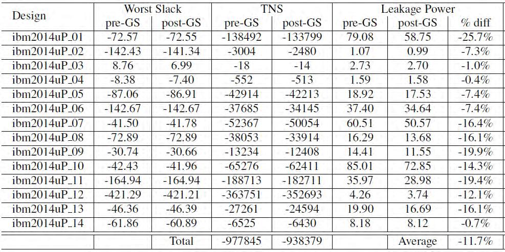
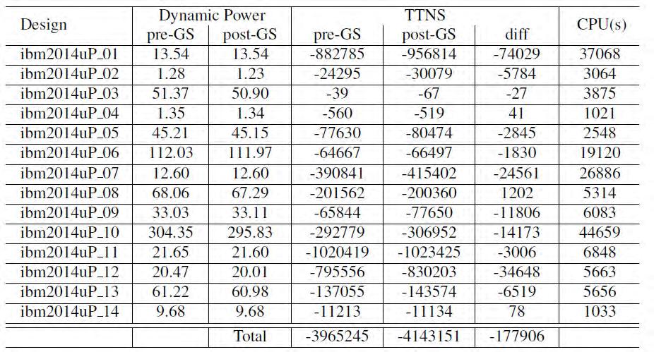
24 Preliminary Results 11.7% average leakage power improvement Up to 25.7% improvement Improvements obtained after a power-driven flow run TNS and worst slack show same input state quality or even improvements TTNS presents significant degradation. A better formulation for the greedy methods is still needed
25 Characteristics needed in a powerdriven cell selection algorithm Runtime scalability Typical runtime of sizing algorithms using signoff timing engines is too long for practical use. Preserve timing quality of results It is unacceptable that TTNS gets degraded significantly during power reduction. Incremental optimization The algorithm has to be able to recognize the existing cell type and timing quality of results, especially for non-critical subpaths with negative slacks.
26 Conclusions Need of new timing-constrained cell selection algorithms for power reduction, where the focus is at the integration into a physical synthesis flow. Experimental results show promising power saving based on a contest-winning LR-based algorithm. 11.7% average leakage power improvement with up to 25.7% improvement. There is much room to improve the power dissipation of our state-of-the-art physical synthesis flow. We detailed our experience in adopting the ISPD2013 winner algorithm while discussed real concerns and issues which have not been seen in the literature.
27 Tiago Reimann Cliff Sze Ricardo Reis Gate Sizing and Threshold Voltage Assignment for High Performance Microprocessor Designs
Leakage Power Minimization in Deep-Submicron CMOS circuits
 Outline Leakage Power Minimization in Deep-Submicron circuits Politecnico di Torino Dip. di Automatica e Informatica 1019 Torino, Italy enrico.macii@polito.it Introduction. Design for low leakage: Basics.
ICCAD 2014 Contest Incremental Timing-driven Placement: Timing Modeling and File Formats v1.1 April 14 th, 2014
 ICCAD 2014 Contest Incremental Timing-driven Placement: Timing Modeling and File Formats v1.1 April 14 th, 2014 http://cad contest.ee.ncu.edu.tw/cad-contest-at-iccad2014/problem b/ 1 Introduction This
Low Power 3-2 and 4-2 Adder Compressors Implemented Using ASTRAN
 XXVII SIM - South Symposium on Microelectronics 1 Low Power 3-2 and 4-2 Adder Compressors Implemented Using ASTRAN Jorge Tonfat, Ricardo Reis jorgetonfat@ieee.org, reis@inf.ufrgs.br Grupo de Microeletrônica
ISSN:
 1061 Area Leakage Power and delay Optimization BY Switched High V TH Logic UDAY PANWAR 1, KAVITA KHARE 2 12 Department of Electronics and Communication Engineering, MANIT, Bhopal 1 panwaruday1@gmail.com,
Timing analysis can be done right after synthesis. But it can only be accurately done when layout is available
 Timing Analysis Lecture 9 ECE 156A-B 1 General Timing analysis can be done right after synthesis But it can only be accurately done when layout is available Timing analysis at an early stage is not accurate
LSI Design Flow Development for Advanced Technology
 LSI Design Flow Development for Advanced Technology Atsushi Tsuchiya LSIs that adopt advanced technologies, as represented by imaging LSIs, now contain 30 million or more logic gates and the scale is beginning
CS 6135 VLSI Physical Design Automation Fall 2003
 CS 6135 VLSI Physical Design Automation Fall 2003 1 Course Information Class time: R789 Location: EECS 224 Instructor: Ting-Chi Wang ( ) EECS 643, (03) 5742963 tcwang@cs.nthu.edu.tw Office hours: M56R5
Minimization of Dynamic and Static Power Through Joint Assignment of Threshold Voltages and Sizing Optimization
 Minimization of Dynamic and Static Power Through Joint Assignment of Threshold Voltages and Sizing Optimization David Nguyen, Abhijit Davare, Michael Orshansky, David Chinnery, Brandon Thompson, and Kurt
THERE is a growing need for high-performance and. Static Leakage Reduction Through Simultaneous V t /T ox and State Assignment
 1014 IEEE TRANSACTIONS ON COMPUTER-AIDED DESIGN OF INTEGRATED CIRCUITS AND SYSTEMS, VOL. 24, NO. 7, JULY 2005 Static Leakage Reduction Through Simultaneous V t /T ox and State Assignment Dongwoo Lee, Student
Low-Power VLSI. Seong-Ook Jung VLSI SYSTEM LAB, YONSEI University School of Electrical & Electronic Engineering
 Low-Power VLSI Seong-Ook Jung 2013. 5. 27. sjung@yonsei.ac.kr VLSI SYSTEM LAB, YONSEI University School of Electrical & Electronic Engineering Contents 1. Introduction 2. Power classification & Power performance
Static Timing Analysis Taking Crosstalk into Account 1
 Static Timing Analysis Taking Crosstalk into Account 1 Matthias Ringe IBM Deutschland Entwicklung GmbH, Schönaicher Str. 220 71032 Böblingen; Germany ringe@de.ibm.com Thomas Lindenkreuz Robert Bosch GmbH,
Low Power Design Part I Introduction and VHDL design. Ricardo Santos LSCAD/FACOM/UFMS
 Low Power Design Part I Introduction and VHDL design Ricardo Santos ricardo@facom.ufms.br LSCAD/FACOM/UFMS Motivation for Low Power Design Low power design is important from three different reasons Device
Blockage and Voltage Island-Aware Dual-VDD Buffered Tree Construction
 Blockage and Voltage Island-Aware Dual-VDD Buffered Tree Construction Bruce Tseng Faraday Technology Cor. Hsinchu, Taiwan Hung-Ming Chen Dept of EE National Chiao Tung U. Hsinchu, Taiwan April 14, 2008
On Chip Active Decoupling Capacitors for Supply Noise Reduction for Power Gating and Dynamic Dual Vdd Circuits in Digital VLSI
 ELEN 689 606 Techniques for Layout Synthesis and Simulation in EDA Project Report On Chip Active Decoupling Capacitors for Supply Noise Reduction for Power Gating and Dynamic Dual Vdd Circuits in Digital
AI Plays Yun Nie (yunn), Wenqi Hou (wenqihou), Yicheng An (yicheng)
, Wenqi Hou (wenqihou), Yicheng An (yicheng)") AI Plays 2048 Yun Nie (yunn), Wenqi Hou (wenqihou), Yicheng An (yicheng) Abstract The strategy game 2048 gained great popularity quickly. Although it is easy to play, people cannot win the game easily,
AI Plays 2048 Yun Nie (yunn), Wenqi Hou (wenqihou), Yicheng An (yicheng) Abstract The strategy game 2048 gained great popularity quickly. Although it is easy to play, people cannot win the game easily,
Optimization of Overdrive Signoff
 Optimization of Overdrive Signoff Tuck-Boon Chan, Andrew B. Kahng, Jiajia Li and Siddhartha Nath VLSI CAD LABORATORY, UC San Diego UC San Diego / VLSI CAD Laboratory -1- Outline Motivation Design Cone
Fast Placement Optimization of Power Supply Pads
 Fast Placement Optimization of Power Supply Pads Yu Zhong Martin D. F. Wong Dept. of Electrical and Computer Engineering Dept. of Electrical and Computer Engineering Univ. of Illinois at Urbana-Champaign
Modeling the Effect of Wire Resistance in Deep Submicron Coupled Interconnects for Accurate Crosstalk Based Net Sorting
 Modeling the Effect of Wire Resistance in Deep Submicron Coupled Interconnects for Accurate Crosstalk Based Net Sorting C. Guardiani, C. Forzan, B. Franzini, D. Pandini Adanced Research, Central R&D, DAIS,
Electronic Design Automation at Transistor Level by Ricardo Reis. Preamble
 1 Electronic Design Automation at Transistor Level by Ricardo Reis Preamble 1 Quintillion of Transistors 90 65 45 32 NM Electronic Design Automation at Transistor Level Ricardo Reis Universidade Federal
Interconnect-Power Dissipation in a Microprocessor
 4/2/2004 Interconnect-Power Dissipation in a Microprocessor N. Magen, A. Kolodny, U. Weiser, N. Shamir Intel corporation Technion - Israel Institute of Technology 4/2/2004 2 Interconnect-Power Definition
Domino Static Gates Final Design Report
 Domino Static Gates Final Design Report Krishna Santhanam bstract Static circuit gates are the standard circuit devices used to build the major parts of digital circuits. Dynamic gates, such as domino
RECENT technology trends have lead to an increase in
 IEEE JOURNAL OF SOLID-STATE CIRCUITS, VOL. 39, NO. 9, SEPTEMBER 2004 1581 Noise Analysis Methodology for Partially Depleted SOI Circuits Mini Nanua and David Blaauw Abstract In partially depleted silicon-on-insulator
Placement and Routing of RF Embedded Passive Designs In LCP Substrate
 Placement and Routing of RF Embedded Passive Designs In LCP Substrate Mohit Pathak, Souvik Mukherjee, Madhavan Swaminathan, Ege Engin, and Sung Kyu Lim School of Electrical and Computer Engineering Georgia
Revisiting the Linear Programming Framework for Leakage Power vs. PerformanceOptimization
 Revisiting the Linear Programming Framework for Leakage Power vs. PerformanceOptimization Kwangok Jeong, Andrew B. Kahng, Hailong Yao CSE and ECE Departments,Universityof California at San Diego kjeong@vlsicad.ucsd.edu,
PROCESS-VOLTAGE-TEMPERATURE (PVT) VARIATIONS AND STATIC TIMING ANALYSIS
 VARIATIONS AND STATIC TIMING ANALYSIS") PROCESS-VOLTAGE-TEMPERATURE (PVT) VARIATIONS AND STATIC TIMING ANALYSIS The major design challenges of ASIC design consist of microscopic issues and macroscopic issues [1]. The microscopic issues are ultra-high
PROCESS-VOLTAGE-TEMPERATURE (PVT) VARIATIONS AND STATIC TIMING ANALYSIS The major design challenges of ASIC design consist of microscopic issues and macroscopic issues [1]. The microscopic issues are ultra-high
Improved DFT for Testing Power Switches
 Improved DFT for Testing Power Switches Saqib Khursheed, Sheng Yang, Bashir M. Al-Hashimi, Xiaoyu Huang School of Electronics and Computer Science University of Southampton, UK. Email: {ssk, sy8r, bmah,
CS250 VLSI Systems Design. Lecture 3: Physical Realities: Beneath the Digital Abstraction, Part 1: Timing
 CS250 VLSI Systems Design Lecture 3: Physical Realities: Beneath the Digital Abstraction, Part 1: Timing Fall 2010 Krste Asanovic, John Wawrzynek with John Lazzaro and Yunsup Lee (TA) What do Computer
EDA Challenges for Low Power Design. Anand Iyer, Cadence Design Systems
 EDA Challenges for Low Power Design Anand Iyer, Cadence Design Systems Agenda Introduction ti LP techniques in detail Challenges to low power techniques Guidelines for choosing various techniques Why is
Clock Tree Power reduction by clock latency reduction. By Sunny Arora, Naveen Sampath, Shilpa Gupta, Sunit Bansal, Ateet Mishra. 8ns. 8ns B.
 Clock Tree Power reduction by clock latency reduction By Sunny Arora, Naveen Sampath, Shilpa Gupta, Sunit Baal, Ateet Mishra Abstract The Current Clock Tree Synthesis strategy used in chips target to build
Towards PVT-Tolerant Glitch-Free Operation in FPGAs
 Towards PVT-Tolerant Glitch-Free Operation in FPGAs Safeen Huda and Jason H. Anderson ECE Department, University of Toronto, Canada 24 th ACM/SIGDA International Symposium on FPGAs February 22, 2016 Motivation
an Intuitive Logic Shifting Heuristic for Improving Timing Slack Violating Paths
 an Intuitive Logic Shifting Heuristic for Improving Timing Slack Violating Paths Xing Wei, Wai-Chung Tang, Yu-Liang Wu Department of Computer Science and Engineering The Chinese University of Hong Kong
Review and Analysis of Glitch Reduction for Low Power VLSI Circuits
 Review and Analysis of Glitch Reduction for Low Power VLSI Circuits Somashekhar Malipatil 1 1 Assistant Professor Department of Electronics & Communication Engineering Nalla Malla Reddy Engineering College,
Control Synthesis and Delay Sensor Deployment for Efficient ASV designs
 Control Synthesis and Delay Sensor Deployment for Efficient ASV designs C H A O FA N L I < C H AO F @ TA M U. E D U >, T E X A S A & M U N I V E RS I T Y S A C H I N S. S A PAT N E K A R, U N I V E RS
A 0.9 V Low-power 16-bit DSP Based on a Top-down Design Methodology
 UDC 621.3.049.771.14:621.396.949 A 0.9 V Low-power 16-bit DSP Based on a Top-down Design Methodology VAtsushi Tsuchiya VTetsuyoshi Shiota VShoichiro Kawashima (Manuscript received December 8, 1999) A 0.9
UNIT-III POWER ESTIMATION AND ANALYSIS
 UNIT-III POWER ESTIMATION AND ANALYSIS In VLSI design implementation simulation software operating at various levels of design abstraction. In general simulation at a lower-level design abstraction offers
A Novel Latch design for Low Power Applications
 A Novel Latch design for Low Power Applications Abhilasha Deptt. of Electronics and Communication Engg., FET-MITS Lakshmangarh, Rajasthan (India) K. G. Sharma Suresh Gyan Vihar University, Jagatpura, Jaipur,
CHAPTER 3 NEW SLEEPY- PASS GATE
 56 CHAPTER 3 NEW SLEEPY- PASS GATE 3.1 INTRODUCTION A circuit level design technique is presented in this chapter to reduce the overall leakage power in conventional CMOS cells. The new leakage po leepy-
Energy Efficient Scheduling Techniques For Real-Time Embedded Systems
 Energy Efficient Scheduling Techniques For Real-Time Embedded Systems Rabi Mahapatra & Wei Zhao This work was done by Rajesh Prathipati as part of his MS Thesis here. The work has been update by Subrata
New Approaches to Total Power Reduction Including Runtime Leakage. Leakage
 1 0 0 % 8 0 % 6 0 % 4 0 % 2 0 % 0 % - 2 0 % - 4 0 % - 6 0 % New Approaches to Total Power Reduction Including Runtime Leakage Dennis Sylvester University of Michigan, Ann Arbor Electrical Engineering and
SURVEY AND EVALUATION OF LOW-POWER FULL-ADDER CELLS
 SURVEY ND EVLUTION OF LOW-POWER FULL-DDER CELLS hmed Sayed and Hussain l-saad Department of Electrical & Computer Engineering University of California Davis, C, U.S.. STRCT In this paper, we survey various
Low Power High Performance 10T Full Adder for Low Voltage CMOS Technology Using Dual Threshold Voltage
 Low Power High Performance 10T Full Adder for Low Voltage CMOS Technology Using Dual Threshold Voltage Surbhi Kushwah 1, Shipra Mishra 2 1 M.Tech. VLSI Design, NITM College Gwalior M.P. India 474001 2
POWER GATING. Power-gating parameters
 POWER GATING Power Gating is effective for reducing leakage power [3]. Power gating is the technique wherein circuit blocks that are not in use are temporarily turned off to reduce the overall leakage
Ramon Canal NCD Master MIRI. NCD Master MIRI 1
 Wattch, Hotspot, Hotleakage, McPAT http://www.eecs.harvard.edu/~dbrooks/wattch-form.html http://lava.cs.virginia.edu/hotspot http://lava.cs.virginia.edu/hotleakage http://www.hpl.hp.com/research/mcpat/
Glitch Power Reduction for Low Power IC Design
 This document is an author-formatted work. The definitive version for citation appears as: N. Weng, J. S. Yuan, R. F. DeMara, D. Ferguson, and M. Hagedorn, Glitch Power Reduction for Low Power IC Design,
High Speed Low Power Noise Tolerant Multiple Bit Adder Circuit Design Using Domino Logic
 High Speed Low Power Noise Tolerant Multiple Bit Adder Circuit Design Using Domino Logic M.Manikandan 2,Rajasri 2,A.Bharathi 3 Assistant Professor, IFET College of Engineering, Villupuram, india 1 M.E,
Measurement and Optimization of Electrical Process Window
 Measurement and Optimization of Electrical Process Window Tuck-Boon Chan*, Abde Ali Kagalwalla, Puneet Gupta Dept. of EE, University of California Los Angeles (tuckie@ee.ucla.edu) Work partly supported
ECE 551: Digital System Design & Synthesis
 ECE 551: Digital System Design & Synthesis Lecture Set 9 9.1: Constraints and Timing 9.2: Optimization (In separate file) 03/30/03 1 ECE 551 - Digital System Design & Synthesis Lecture 9.1 - Constraints
A Dual-V DD Low Power FPGA Architecture
 A Dual-V DD Low Power FPGA Architecture A. Gayasen 1, K. Lee 1, N. Vijaykrishnan 1, M. Kandemir 1, M.J. Irwin 1, and T. Tuan 2 1 Dept. of Computer Science and Engineering Pennsylvania State University
Dr. Ralf Sommer. Munich, March 8th, 2006 COM BTS DAT DF AMF. Presenter Dept Titel presentation Date Page 1
 DATE 2006 Special Session: DFM/DFY Design for Manufacturability and Yield - Influence of Process Variations in Digital, Analog and Mixed-Signal Circuit Design DATE 06 Munich, March 8th, 2006 Presenter
Andrew Clinton, Matt Liberty, Ian Kuon
 Andrew Clinton, Matt Liberty, Ian Kuon FPGA Routing (Interconnect) FPGA routing consists of a network of wires and programmable switches Wire is modeled with a reduced RC network Drivers are modeled as
Chapter 1 Introduction
 Chapter 1 Introduction 1.1 Introduction There are many possible facts because of which the power efficiency is becoming important consideration. The most portable systems used in recent era, which are
Lecture 10. Circuit Pitfalls
 Lecture 10 Circuit Pitfalls Intel Corporation jstinson@stanford.edu 1 Overview Reading Lev Signal and Power Network Integrity Chandrakasen Chapter 7 (Logic Families) and Chapter 8 (Dynamic logic) Gronowski
Short-Circuit Power Reduction by Using High-Threshold Transistors
 J. Low Power Electron. Appl. 2012, 2, 69-78; doi:10.3390/jlpea2010069 OPEN ACCESS Journal of Low Power Electronics and Applications ISSN 2079-9268 www.mdpi.com/journal/jlpea/ Article Short-Circuit Power
Low Power System-On-Chip-Design Chapter 12: Physical Libraries
 1 Low Power System-On-Chip-Design Chapter 12: Physical Libraries Friedemann Wesner 2 Outline Standard Cell Libraries Modeling of Standard Cell Libraries Isolation Cells Level Shifters Memories Power Gating
Low Power Design Methods: Design Flows and Kits
 JOINT ADVANCED STUDENT SCHOOL 2011, Moscow Low Power Design Methods: Design Flows and Kits Reported by Shushanik Karapetyan Synopsys Armenia Educational Department State Engineering University of Armenia
Physical Design of Monolithic 3D ICs with Applications to Hardware Security
 Physical Design of Monolithic ICs with Applications to Hardware Security Chen Yan and Emre Salman Department of Electrical and Computer Engineering Stony Brook University (SUNY), Stony Brook, NY 11794
Full-chip Multilevel Routing for Power and Signal Integrity
 Full-chip Multilevel Routing for Power and Signal Integrity Jinjun Xiong and Lei He Electrical Engineering Department University of California at Los Angeles, CA, USA Abstract Conventional physical design
MS Project :Trading Accuracy for Power with an Under-designed Multiplier Architecture Parag Kulkarni Adviser : Prof. Puneet Gupta Electrical Eng.
 MS Project :Trading Accuracy for Power with an Under-designed Multiplier Architecture Parag Kulkarni Adviser : Prof. Puneet Gupta Electrical Eng., UCLA - http://nanocad.ee.ucla.edu/ 1 Outline Introduction
UNIVERSITY OF CALIFORNIA College of Engineering Department of Electrical Engineering and Computer Sciences
 UNIVERSITY OF CALIFORNIA College of Engineering Department of Electrical Engineering and Computer Sciences Jan Rabaey EECS 141 Spring 2010 LDPC Decoder Project Phase 3 Due Noon, Wednesday, May 5th, 2010
Lecture 11: Clocking
 High Speed CMOS VLSI Design Lecture 11: Clocking (c) 1997 David Harris 1.0 Introduction We have seen that generating and distributing clocks with little skew is essential to high speed circuit design.
Physical Design of Digital Integrated Circuits (EN0291 S40) Sherief Reda Division of Engineering, Brown University Fall 2006
 Sherief Reda Division of Engineering, Brown University Fall 2006") Physical Design of Digital Integrated Circuits (EN0291 S40) Sherief Reda Division of Engineering, Brown University Fall 2006 Lecture 01: the big picture Course objective Brief tour of IC physical design
Physical Design of Digital Integrated Circuits (EN0291 S40) Sherief Reda Division of Engineering, Brown University Fall 2006 Lecture 01: the big picture Course objective Brief tour of IC physical design
Resonant Clock Circuits for Energy Recovery Power Reductions
 Resonant Clock Circuits for Energy Recovery Power Reductions Riadul Islam Ignatius Bezzam SCHOOL OF ENGINEERING CLOCKING CHALLENGE Synchronous operation needs low clock skew across chip High Performance
Single Event Transient Effects on Microsemi ProASIC Flash-based FPGAs: analysis and possible solutions
 Single Event Transient Effects on Microsemi ProASIC Flash-based FPGAs: analysis and possible solutions L. Sterpone Dipartimento di Automatica e Informatica Politecnico di Torino, Torino, ITALY 1 Motivations
Keywords : MTCMOS, CPFF, energy recycling, gated power, gated ground, sleep switch, sub threshold leakage. GJRE-F Classification : FOR Code:
 Global Journal of researches in engineering Electrical and electronics engineering Volume 12 Issue 3 Version 1.0 March 2012 Type: Double Blind Peer Reviewed International Research Journal Publisher: Global
Cost-Effective Radiation Hardening Technique for Combinational Logic
 Cost-Effective Radiation Hardening Technique for Combinational Logic Quming Zhou and Kartik Mohanram Department of Electrical and Computer Engineering Rice University, Houston, TX 775 {quming, kmram}@rice.edu
AN EFFICIENT APPROACH TO MINIMIZE POWER AND AREA IN CARRY SELECT ADDER USING BINARY TO EXCESS ONE CONVERTER
 AN EFFICIENT APPROACH TO MINIMIZE POWER AND AREA IN CARRY SELECT ADDER USING BINARY TO EXCESS ONE CONVERTER K. RAMAMOORTHY 1 T. CHELLADURAI 2 V. MANIKANDAN 3 1 Department of Electronics and Communication
Energy Efficiency of Power-Gating in Low-Power Clocked Storage Elements
 Energy Efficiency of Power-Gating in Low-Power Clocked Storage Elements Christophe Giacomotto 1, Mandeep Singh 1, Milena Vratonjic 1, Vojin G. Oklobdzija 1 1 Advanced Computer systems Engineering Laboratory,
A HIGH SPEED & LOW POWER 16T 1-BIT FULL ADDER CIRCUIT DESIGN BY USING MTCMOS TECHNIQUE IN 45nm TECHNOLOGY
 A HIGH SPEED & LOW POWER 16T 1-BIT FULL ADDER CIRCUIT DESIGN BY USING MTCMOS TECHNIQUE IN 45nm TECHNOLOGY Jasbir kaur 1, Neeraj Singla 2 1 Assistant Professor, 2 PG Scholar Electronics and Communication
Ruixing Yang
 Design of the Power Switching Network Ruixing Yang 15.01.2009 Outline Power Gating implementation styles Sleep transistor power network synthesis Wakeup in-rush current control Wakeup and sleep latency
induced Aging g Co-optimization for Digital ICs
 International Workshop on Emerging g Circuits and Systems (2009) Leakage power and NBTI- induced Aging g Co-optimization for Digital ICs Yu Wang Assistant Prof. E.E. Dept, Tsinghua University, China On-going
An Enhanced Design Methodology for Resonant Clock. Trees
 An Enhanced Design Methodology for Resonant Clock Trees Somayyeh Rahimian, Vasilis Pavlidis, Xifan Tang, and Giovanni De Micheli Abstract Clock distribution networks consume a considerable portion of the
A COMPARATIVE ANALYSIS OF LEAKAGE REDUCTION TECHNIQUES IN NANOSCALE CMOS ARITHMETIC CIRCUITS
 1 A COMPARATIVE ANALYSIS OF LEAKAGE REDUCTION TECHNIQUES IN NANOSCALE CMOS ARITHMETIC CIRCUITS Frank Anthony Hurtado and Eugene John Department of Electrical and Computer Engineering The University of
Low-Power Digital CMOS Design: A Survey
 Low-Power Digital CMOS Design: A Survey Krister Landernäs June 4, 2005 Department of Computer Science and Electronics, Mälardalen University Abstract The aim of this document is to provide the reader with
Energy-Recovery CMOS Design
 Energy-Recovery CMOS Design Jay Moon, Bill Athas * Univ of Southern California * Apple Computer, Inc. jsmoon@usc.edu / athas@apple.com March 05, 2001 UCLA EE215B jsmoon@usc.edu / athas@apple.com 1 Outline
Dual-Threshold Voltage Assignment with Transistor Sizing for Low Power CMOS Circuits
 390 IEEE TRANSACTIONS ON VERY LARGE SCALE INTEGRATION (VLSI) SYSTEMS, VOL. 9, NO. 2, APRIL 2001 Dual-Threshold Voltage Assignment with Transistor Sizing for Low Power CMOS Circuits TABLE I RESULTS FOR
Power Supply Networks: Analysis and Synthesis. What is Power Supply Noise?
 Power Supply Networs: Analysis and Synthesis What is Power Supply Noise? Problem: Degraded voltage level at the delivery point of the power/ground grid causes performance and/or functional failure Lower
Managing Metastability with the Quartus II Software
 Managing Metastability with the Quartus II Software 13 QII51018 Subscribe You can use the Quartus II software to analyze the average mean time between failures (MTBF) due to metastability caused by synchronization
Decoupling Capacitance
 Decoupling Capacitance Nitin Bhardwaj ECE492 Department of Electrical and Computer Engineering Agenda Background On-Chip Algorithms for decap sizing and placement Based on noise estimation Decap modeling
Low Power Techniques for SoC Design: basic concepts and techniques
 Low Power Techniques for SoC Design: basic concepts and techniques Estagiário de Docência M.Sc. Vinícius dos Santos Livramento Prof. Dr. Luiz Cláudio Villar dos Santos Embedded Systems - INE 5439 Federal
Propagation Delay, Circuit Timing & Adder Design. ECE 152A Winter 2012
 Propagation Delay, Circuit Timing & Adder Design ECE 152A Winter 2012 Reading Assignment Brown and Vranesic 2 Introduction to Logic Circuits 2.9 Introduction to CAD Tools 2.9.1 Design Entry 2.9.2 Synthesis
Propagation Delay, Circuit Timing & Adder Design
 Propagation Delay, Circuit Timing & Adder Design ECE 152A Winter 2012 Reading Assignment Brown and Vranesic 2 Introduction to Logic Circuits 2.9 Introduction to CAD Tools 2.9.1 Design Entry 2.9.2 Synthesis
Approximating Computation and Data for Energy Efficiency
 Approximating Computation and Data for Energy Efficiency Daniele Jahier Pagliari EDA Group Politecnico di Torino Torino, Italy 1st IWES September 20th, 2016, Pisa, Italy Outline Error Tolerance and Approximate
Gateways Placement in Backbone Wireless Mesh Networks
 I. J. Communications, Network and System Sciences, 2009, 1, 1-89 Published Online February 2009 in SciRes (http://www.scirp.org/journal/ijcns/). Gateways Placement in Backbone Wireless Mesh Networks Abstract
EECS 427 Lecture 13: Leakage Power Reduction Readings: 6.4.2, CBF Ch.3. EECS 427 F09 Lecture Reminders
 EECS 427 Lecture 13: Leakage Power Reduction Readings: 6.4.2, CBF Ch.3 [Partly adapted from Irwin and Narayanan, and Nikolic] 1 Reminders CAD assignments Please submit CAD5 by tomorrow noon CAD6 is due
Wide Fan-In Gates for Combinational Circuits Using CCD
 Wide Fan-In Gates for Combinational Circuits Using CCD Mekala.S Post Graduate Scholar, Nandha Engineering College, Erode, Tamil Nadu, India Abstract: A new domino circuit is proposed with low leakage and
Scheduling and Communication Synthesis for Distributed Real-Time Systems
 Scheduling and Communication Synthesis for Distributed Real-Time Systems Department of Computer and Information Science Linköpings universitet 1 of 30 Outline Motivation System Model and Architecture Scheduling
Delay of different load cap. v.s. different sizes of cells 1.6. Delay of different cells (ns)
") Cell Selection from Technology Libraries for Minimizing Power Yumin Zhang Synopsys, Inc. 700 East Middlefield Road Mountain View, CA 94043 yumin@synopsys.com Xiaobo (Sharon) Hu Danny Z. Chen Department
Cell Selection from Technology Libraries for Minimizing Power Yumin Zhang Synopsys, Inc. 700 East Middlefield Road Mountain View, CA 94043 yumin@synopsys.com Xiaobo (Sharon) Hu Danny Z. Chen Department
EE 434 ASIC and Digital Systems. Prof. Dae Hyun Kim School of Electrical Engineering and Computer Science Washington State University.
 EE 434 ASIC and Digital Systems Prof. Dae Hyun Kim School of Electrical Engineering and Computer Science Washington State University Preliminaries VLSI Design System Specification Functional Design RTL
Design of High Performance Arithmetic and Logic Circuits in DSM Technology
 Design of High Performance Arithmetic and Logic Circuits in DSM Technology Salendra.Govindarajulu 1, Dr.T.Jayachandra Prasad 2, N.Ramanjaneyulu 3 1 Associate Professor, ECE, RGMCET, Nandyal, JNTU, A.P.Email:
Chapter 3 Chip Planning
 Chapter 3 Chip Planning 3.1 Introduction to Floorplanning 3. Optimization Goals in Floorplanning 3.3 Terminology 3.4 Floorplan Representations 3.4.1 Floorplan to a Constraint-Graph Pair 3.4. Floorplan
Activity-Aware Registers Placement for Low Power Gated Clock Tree Construction
 Activity-Aware Registers Placement for Low Power Gated Clock Tree Construction Weixiang Shen, Yici Cai, Xianlong Hong Dept. of Computer Science & Technology Tsinghua University Beijing, 100084, P. R. China
PV-PPV: Parameter Variability Aware, Automatically Extracted, Nonlinear Time-Shifted Oscillator Macromodels
 PV-PPV: Parameter Variability Aware, Automatically Extracted, Nonlinear Time-Shifted Oscillator Macromodels Zhichun Wang, Xiaolue Lai and Jaijeet Roychowdhury Dept of ECE, University of Minnesota, Twin
Synthesis of Low Power CED Circuits Based on Parity Codes
 Synthesis of Low CED Circuits Based on Parity Codes Shalini Ghosh 1, Sugato Basu 2, and Nur A. Touba 1 1 Dept. of Electrical and Computer Engineering, University of Texas, Austin, TX 78712 {shalini,touba}@ece.utexas.edu
Amber Path FX SPICE Accurate Statistical Timing for 40nm and Below Traditional Sign-Off Wastes 20% of the Timing Margin at 40nm
 Amber Path FX SPICE Accurate Statistical Timing for 40nm and Below Amber Path FX is a trusted analysis solution for designers trying to close on power, performance, yield and area in 40 nanometer processes
Power Spring /7/05 L11 Power 1
 Power 6.884 Spring 2005 3/7/05 L11 Power 1 Lab 2 Results Pareto-Optimal Points 6.884 Spring 2005 3/7/05 L11 Power 2 Standard Projects Two basic design projects Processor variants (based on lab1&2 testrigs)
Semiconductor Technology Academic Research Center An RTL-to-GDS2 Design Methodology for Advanced System LSI
 Semiconductor Technology Academic Research Center An RTL-to-GDS2 Design Methodology for Advanced System LSI Jan. 28. 2011 Nobuyuki Nishiguchi Semiconductor Technology Advanced Research Center (STARC) ASP-DAC
The Need for Gate-Level CDC
 The Need for Gate-Level CDC Vikas Sachdeva Real Intent Inc., Sunnyvale, CA I. INTRODUCTION Multiple asynchronous clocks are a fact of life in today s SoC. Individual blocks have to run at different speeds
Overview of Design Methodology. A Few Points Before We Start 11/4/2012. All About Handling The Complexity. Lecture 1. Put things into perspective
 Overview of Design Methodology Lecture 1 Put things into perspective ECE 156A 1 A Few Points Before We Start ECE 156A 2 All About Handling The Complexity Design and manufacturing of semiconductor products
A Survey of the Low Power Design Techniques at the Circuit Level
 A Survey of the Low Power Design Techniques at the Circuit Level Hari Krishna B Assistant Professor, Department of Electronics and Communication Engineering, Vagdevi Engineering College, Warangal, India
INTERNATIONAL JOURNAL OF PURE AND APPLIED RESEARCH IN ENGINEERING AND TECHNOLOGY
 INTERNATIONAL JOURNAL OF PURE AND APPLIED RESEARCH IN ENGINEERING AND TECHNOLOGY A PATH FOR HORIZING YOUR INNOVATIVE WORK DESIGN OF PD AND HIGH PERFORMANCE VCO FOR PLL WITH 45 nm CMOS TECHNOLOGY VAISHALI