Learning Outcomes. Spiral 2 8. Digital Design Overview LAYOUT
|
|
|
- Cordelia Short
- 6 years ago
- Views:
Transcription
1 Spiral 2 8 Cell Mark Redekopp earning Outcomes I understand how a digital circuit is composed of layers of materials forming transistors and wires I understand how each layer is expressed as geometric patterns called masks I understand the difference between custom and standard cell SIC flow I understand how FPGs implement arbitrary logic designs by producing a bit stream which is the contents of ook Up Tables and mux selects I understand the pros and cons of SIC vs. FPG design targets igital esign Overview Circuit esign esign Partitioning YOUT Verify the circuitry logic Compile a netlist Floorplanning Placement Routing flowchart of digital From concept through testing and finally to a layout
2 We need to describe the patterns of material to deposit and build on the silicon surface We will draw it from a top down perspective Source Input W Gate Input rain Output n-type p-type Below is a notional layout of two inverters back to back et's go through the steps for how we would lay this out ~ Start with p type substrate which is what we need for NMOS dd n well area for the PMOS transistors N Well P Type Now we lay down the n and p diffusion areas for the source and drain of both NMOS and PMOS Notice the W/ relationship Right now the length seems longer than it really will be p+ diff n+ diff. W W


3 Now we draw the polysilicon gates Poly Now we add the 1 metal (M1) wires which include the and rail as well as the input and output signals To make a connection from the M1 level to the surface of the chip we add contacts M1 Contact ~ M2 Mn CMOS Inverter Taps in (b) to connect n well and p substrate to V and ground respectively How do we get out from between and Gnd? We need another level of metal, M2 M2 Just like a freeway interchange ~ 12


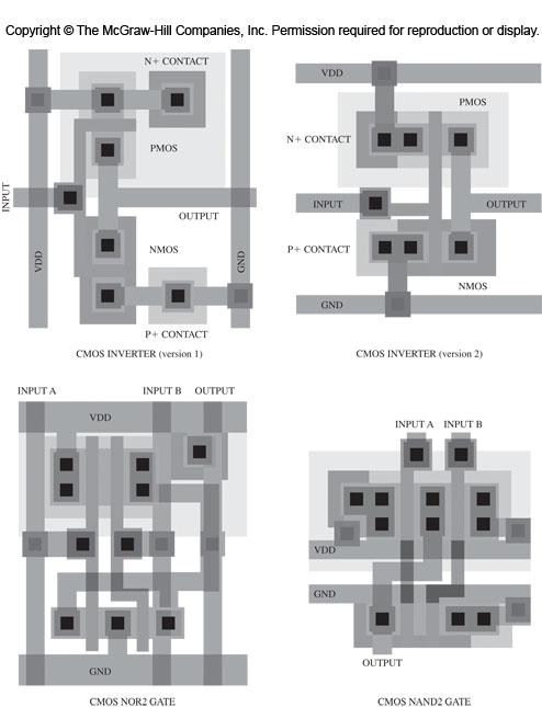
4 NN and NOR Gate CMOS Gates Inverter, NN2, NOR Two sample layouts of CMOS inverter circuits (for p-type substrate) students/adamsk5/lab6/nor_lay_sim.jpg 14 Chips re 3 Sandwiches Ensuring we can fabricate a working chip ESIGN RUES


 to verify")


 ESIGN FOW Verify the")
5 Reminder: esign Rules ambda Rules: One lambda = one half of the minimum mask dimension, typically the length of a transistor channel ambda Rules are based on the assumption that one can scale a design to the appropriate size before manufacturing Every spacing and sizing value is presented based on multiples of lambda The layout tool has a design rule checker (RC) to verify those. In case of any violations the tool will point that out nmos and pmos transistors in series, and in parallel, respectively CMOS NN igital esign Overview Circuit esign esign Partitioning CUSTOM OR STNR CE SIC (NOT FPG) ESIGN FOW Verify the circuitry logic Compile a netlist Floorplanning Placement Routing flowchart of digital From concept through testing and finally to a layout


6 esign fter circuit design, we obtain a netlist which could be easily translated into a schematic. Now, let s start the layout design (a.k.a. physical design) Partitioning ivide the chip into smaller blocks This is done based on some goals and constraints, e.g., to minimize the number of connections between the blocks, but in general it is done to separate different functional blocks and simplify their physical design process and also to make placement and routing easier For example, during partitioning you may decide to divide your design into two blocks, such that the total number of connections between the gates in different blocks is minimized Floorplanning Create functional areas for your chip. For example, decide where to place FPU (Floating Point Unit), RM, MPU (Microprocessor), ROM on the chip Place the input and output (I/O) cells of your chip Connect functional blocks with I/O pads or with each other Check whether long wires would slow your design Placement esign (cont.) Nail down the exact positions of all logic gates within each block Place I/O drivers Similarly to other steps, placement is done based on goals and constraints, e.g., such that the total approximate wire length is minimized Routing esign (cont.) Route power nets and clock nets first. They are critical nets Route rest of the nets Routing is typically done in two steps of global routing and detailed routing. In global routing the resource (channels) for the wires are selected and in detailed routing, the wires are assigned to a specific routing track (metal layer) in the selected channels Macro View of a Chip Place and route are very important aspects of design
 that are already laid out at various sizing levels for drive strength (to")
 Example http://web.engr.oregonstate.edu/~traylor/ece474/reading/se_ Cell_ib_Rev1_4_20_1.pdf FPGS 2-8.27 2-8.")
 Circuits 100 s of millions of gates igital esign Targets Two possible implementation targets Custom Chips (SIC s = pplication Specific Integrated Circuits): Physical")
7 Standard Cell ibrary Standard Cell ibrary Intellectual property provided by a vendor Has many pre defined gates (cells) that are already laid out at various sizing levels for drive strength (to achieve desired delay) esign Flow You develop a design synthesis software tool determines what cells are needed place and route tool determines how to place them and route the input/output of each cell appropriately (i.e. using various metal layers) Example Cell_ib_Rev1_4_20_1.pdf FPGS Progression of ogic ensity Small Scale Integrated (SSI) Circuits 1960 s and 1970 s few gates on a chip Medium Scale Integrated (MSI) Circuits 1970 s round a hundred gates per chip ( 283s and 85s) Very arge Scale Integrated (VSI) Circuits 100 s of millions of gates igital esign Targets Two possible implementation targets Custom Chips (SIC s = pplication Specific Integrated Circuits): Physical gates are created on silicon to implement 1 particular design FPG (Field Programmable Gate rray s): Programmable logic using programmable memories to implement logic functions along with other logic resources tiled on the chip. Can implement any design and then be changed to implement a new one In an SIC design, a unique chip will be manufactured that implements our design at which point the HW design is fixed & cannot be changed (example: Pentium, etc.) FPG s have logic resources on them that we can configure to implement our specific design. We can then reconfigure it to implement another design
 rather")


8 SICs Basis of FPG s Memories provide a way to implement a logic function 2 n x m memory can implement a function of If we use RWM (read/write memory) rather than ROM s we can change what function the memory implements Memories are referred to as ook up Tables (UT s) C in Y X x2 Memory Cout S Full dder Implementation Configurable ogic Blocks ( s) Routing & Switch Matrices Writable ook Up Table FF s with bypass path Bypass mux selects the pure combinational output of the UT or the registered/ FF output Blue boxes indicate bits that control the operation and function of the logic 8x2 Mem ny 3-input / 2-output combinational function CK CK FF s if sequential logic needed Inputs and outputs of neighboring s connect to a () Switch matrix is simply composed of that allow us to inputs and outputs to another or further away
9 Routing & Switch Matrices To / from W K J B B... B B Switch Matrix () B... To / from N C E F To / from E Place and Route SIC: Find where each gate should be placed on the chip and how to route the wires that connect to it FPG: etermine which UT s should be used and how to route through switch matrices ffects timing and area wiring takes up space and longer wires leads to longer delays SIC FPG I H G To / from S Exercise Implementation Find the configuration bits to build a 3 bit up counter with enable CE 8x2 Mem CK 1 0 CK CK 8x2 Mem. 1 0 CK SIC s Use the C tools to synthesize and route a netlist Synthesis = Takes logic description or logic schematic & converts to transistor level gates Place and Route = Figure out where each gate should go on the chip) Final netlist is sent to chip maker for production Fabrication is very expensive (> $1 million) so get your design right the first time. FPG s Synthesis converts logic description to necessary UT contents, etc. Place and route produces a configuration for the FPG chip Can reconfigure FPG as much as you like, so less important to get it right 1 st time
 FPG s esigns Expensive Flexible igilent Nexys 2 Board Has a Xilinx Spartan 3E FPG")
10 SIC s vs. FPG s Xilinx Spartan 3E SIC s Handles esigns Expensive Flexible (Cannot be to perform a new hardware function) FPG s esigns Expensive Flexible igilent Nexys 2 Board Has a Xilinx Spartan 3E FPG (XC3S500e) 500K gate equivalent 9312 FF s on board On board I/O (4) 7 Segment isplays (8) E s (4) Push Buttons (8) Switches atest FPG's SoC design (Xilinx Kintex [KU115]) uad Core RM cores R3 SRM Memory Interface ~800 I/O Pins Equiv. ~15M gate equivalent FPG fabric ~1M FFs + 552K UTs 1968 dedicated SP "slices" 18x18 multiply + adder 34.6 Megabits of onboard Block RMs
Lecture 9: Cell Design Issues
 Lecture 9: Cell Design Issues MAH, AEN EE271 Lecture 9 1 Overview Reading W&E 6.3 to 6.3.6 - FPGA, Gate Array, and Std Cell design W&E 5.3 - Cell design Introduction This lecture will look at some of the
Sticks Diagram & Layout. Part II
 Sticks Diagram & Layout Part II Well and Substrate Taps Substrate must be tied to GND and n-well to V DD Metal to lightly-doped semiconductor forms poor connection called Shottky Diode Use heavily doped
Introduction to CMOS VLSI Design (E158) Lecture 9: Cell Design
 Lecture 9: Cell Design") Harris Introduction to CMOS VLSI Design (E158) Lecture 9: Cell Design David Harris Harvey Mudd College David_Harris@hmc.edu Based on EE271 developed by Mark Horowitz, Stanford University MAH E158 Lecture
Harris Introduction to CMOS VLSI Design (E158) Lecture 9: Cell Design David Harris Harvey Mudd College David_Harris@hmc.edu Based on EE271 developed by Mark Horowitz, Stanford University MAH E158 Lecture
CMOS VLSI IC Design. A decent understanding of all tasks required to design and fabricate a chip takes years of experience
 CMOS VLSI IC Design A decent understanding of all tasks required to design and fabricate a chip takes years of experience 1 Commonly used keywords INTEGRATED CIRCUIT (IC) many transistors on one chip VERY
Reference. Wayne Wolf, FPGA-Based System Design Pearson Education, N Krishna Prakash,, Amrita School of Engineering
 FPGA Fabrics Reference Wayne Wolf, FPGA-Based System Design Pearson Education, 2004 CPLD / FPGA CPLD Interconnection of several PLD blocks with Programmable interconnect on a single chip Logic blocks executes
EE141-Spring 2007 Digital Integrated Circuits
 EE141-Spring 2007 Digital Integrated Circuits Lecture 22 I/O, Power Distribution dders 1 nnouncements Homework 9 has been posted Due Tu. pr. 24, 5pm Project Phase 4 (Final) Report due Mo. pr. 30, noon
I/O Design EE141. Announcements. EE141-Fall 2006 Digital Integrated Circuits. Class Material. Pads + ESD Protection.
 EE141-Fall 2006 Digital Integrated Circuits nnouncements Homework 9 due on Thursday Lecture 26 I/O 1 2 Class Material Last lecture Timing Clock distribution Today s lecture I/O Power distribution Intro
Jack Keil Wolf Lecture. ESE 570: Digital Integrated Circuits and VLSI Fundamentals. Lecture Outline. MOSFET N-Type, P-Type.
 ESE 570: Digital Integrated Circuits and VLSI Fundamentals Jack Keil Wolf Lecture Lec 3: January 24, 2019 MOS Fabrication pt. 2: Design Rules and Layout http://www.ese.upenn.edu/about-ese/events/wolf.php
! MOS Device Layout. ! Inverter Layout. ! Gate Layout and Stick Diagrams. ! Design Rules. ! Standard Cells. ! CMOS Process Enhancements
 EE 570: igital Integrated Circuits and VLI Fundamentals Lec 3: January 18, 2018 MO Fabrication pt. 2: esign Rules and Layout Lecture Outline! MO evice Layout! Inverter Layout! Gate Layout and tick iagrams!
ESE 570: Digital Integrated Circuits and VLSI Fundamentals
 ESE 570: Digital Integrated Circuits and VLSI Fundamentals Lec 3: January 24, 2019 MOS Fabrication pt. 2: Design Rules and Layout Penn ESE 570 Spring 2019 Khanna Jack Keil Wolf Lecture http://www.ese.upenn.edu/about-ese/events/wolf.php
Very Large Scale Integration (VLSI)
") Very Large Scale Integration (VLSI) Lecture 6 Dr. Ahmed H. Madian Ah_madian@hotmail.com Dr. Ahmed H. Madian-VLSI 1 Contents Array subsystems Gate arrays technology Sea-of-gates Standard cell Macrocell
Very Large Scale Integration (VLSI) Lecture 6 Dr. Ahmed H. Madian Ah_madian@hotmail.com Dr. Ahmed H. Madian-VLSI 1 Contents Array subsystems Gate arrays technology Sea-of-gates Standard cell Macrocell
Lecture 3, Handouts Page 1. Introduction. EECE 353: Digital Systems Design Lecture 3: Digital Design Flows, Simulation Techniques.
 Introduction EECE 353: Digital Systems Design Lecture 3: Digital Design Flows, Techniques Cristian Grecu grecuc@ece.ubc.ca Course web site: http://courses.ece.ubc.ca/353/ What have you learned so far?
Disseny físic. Disseny en Standard Cells. Enric Pastor Rosa M. Badia Ramon Canal DM Tardor DM, Tardor
 Disseny físic Disseny en Standard Cells Enric Pastor Rosa M. Badia Ramon Canal DM Tardor 2005 DM, Tardor 2005 1 Design domains (Gajski) Structural Processor, memory ALU, registers Cell Device, gate Transistor
Engr354: Digital Logic Circuits
 Engr354: Digital Logic Circuits Chapter 3: Implementation Technology Curtis Nelson Chapter 3 Overview In this chapter you will learn about: How transistors are used as switches; Integrated circuit technology;
Synthesis of Combinational Logic
 Synthesis of ombinational Logic 6.4 Gates F = xor Handouts: Lecture Slides, PS3, Lab2 6.4 - Spring 2 2/2/ L5 Logic Synthesis Review: K-map Minimization ) opy truth table into K-Map 2) Identify subcubes,
! Review: MOS IV Curves and Switch Model. ! MOS Device Layout. ! Inverter Layout. ! Gate Layout and Stick Diagrams. ! Design Rules. !
 ESE 570: Digital Integrated Circuits and VLSI Fundamentals Lec 3: January 21, 2016 MOS Fabrication pt. 2: Design Rules and Layout Lecture Outline! Review: MOS IV Curves and Switch Model! MOS Device Layout!
ESE 570: Digital Integrated Circuits and VLSI Fundamentals
 ESE 570: Digital Integrated Circuits and VLSI Fundamentals Lec 3: January 21, 2016 MOS Fabrication pt. 2: Design Rules and Layout Penn ESE 570 Spring 2016 Khanna Adapted from GATech ESE3060 Slides Lecture
Lecture 0: Introduction
 Lecture 0: Introduction Introduction Integrated circuits: many transistors on one chip. Very Large Scale Integration (VLSI): bucketloads! Complementary Metal Oxide Semiconductor Fast, cheap, low power
420 Intro to VLSI Design
 Dept of Electrical and Computer Engineering 420 Intro to VLSI Design Lecture 0: Course Introduction and Overview Valencia M. Joyner Spring 2005 Getting Started Syllabus About the Instructor Labs, Problem
Homework 10 posted just for practice. Office hours next week, schedule TBD. HKN review today. Your feedback is important!
 EE141 Fall 2005 Lecture 26 Memory (Cont.) Perspectives Administrative Stuff Homework 10 posted just for practice No need to turn in Office hours next week, schedule TBD. HKN review today. Your feedback
+1 (479)
") Introduction to VLSI Design http://csce.uark.edu +1 (479) 575-6043 yrpeng@uark.edu Invention of the Transistor Vacuum tubes ruled in first half of 20th century Large, expensive, power-hungry, unreliable
Introduction to VLSI Design http://csce.uark.edu +1 (479) 575-6043 yrpeng@uark.edu Invention of the Transistor Vacuum tubes ruled in first half of 20th century Large, expensive, power-hungry, unreliable
! Review: MOS IV Curves and Switch Model. ! MOS Device Layout. ! Inverter Layout. ! Gate Layout and Stick Diagrams. ! Design Rules. !
 ESE 570: Digital Integrated Circuits and VLSI Fundamentals Lec 3: January 21, 2017 MOS Fabrication pt. 2: Design Rules and Layout Lecture Outline! Review: MOS IV Curves and Switch Model! MOS Device Layout!
2009 Spring CS211 Digital Systems & Lab 1 CHAPTER 3: TECHNOLOGY (PART 2)
") 1 CHAPTER 3: IMPLEMENTATION TECHNOLOGY (PART 2) Whatwillwelearninthischapter? we learn in this 2 How transistors operate and form simple switches CMOS logic gates IC technology FPGAs and other PLDs Basic
1 CHAPTER 3: IMPLEMENTATION TECHNOLOGY (PART 2) Whatwillwelearninthischapter? we learn in this 2 How transistors operate and form simple switches CMOS logic gates IC technology FPGAs and other PLDs Basic
EE4800 CMOS Digital IC Design & Analysis. Lecture 1 Introduction Zhuo Feng
 EE4800 CMOS Digital IC Design & Analysis Lecture 1 Introduction Zhuo Feng 1.1 Prof. Zhuo Feng Office: EERC 730 Phone: 487-3116 Email: zhuofeng@mtu.edu Class Website http://www.ece.mtu.edu/~zhuofeng/ee4800fall2010.html
Programmable Logic Arrays (PLAs)
") Programmable Logic Regular logic Programmable Logic rrays Multiplexers/ecoders ROMs Field Programmable Gate rrays Xilinx Vertex Random Logic Full ustom esign S 5 - Fall 25 Lec. #3: Programmable Logic -
Programmable Logic Regular logic Programmable Logic rrays Multiplexers/ecoders ROMs Field Programmable Gate rrays Xilinx Vertex Random Logic Full ustom esign S 5 - Fall 25 Lec. #3: Programmable Logic -
Propagation Delay, Circuit Timing & Adder Design. ECE 152A Winter 2012
 Propagation Delay, Circuit Timing & Adder Design ECE 152A Winter 2012 Reading Assignment Brown and Vranesic 2 Introduction to Logic Circuits 2.9 Introduction to CAD Tools 2.9.1 Design Entry 2.9.2 Synthesis
Propagation Delay, Circuit Timing & Adder Design
 Propagation Delay, Circuit Timing & Adder Design ECE 152A Winter 2012 Reading Assignment Brown and Vranesic 2 Introduction to Logic Circuits 2.9 Introduction to CAD Tools 2.9.1 Design Entry 2.9.2 Synthesis
Lecture Perspectives. Administrivia
 Lecture 29-30 Perspectives Administrivia Final on Friday May 18 12:30-3:30 pm» Location: 251 Hearst Gym Topics all what was covered in class. Review Session Time and Location TBA Lab and hw scores to be
CMOS Digital Logic Design with Verilog. Chapter1 Digital IC Design &Technology
 CMOS Digital Logic Design with Verilog Chapter1 Digital IC Design &Technology Chapter Overview: In this chapter we study the concept of digital hardware design & technology. This chapter deals the standard
Lecture 30. Perspectives. Digital Integrated Circuits Perspectives
 Lecture 30 Perspectives Administrivia Final on Friday December 15 8 am Location: 251 Hearst Gym Topics all what was covered in class. Precise reading information will be posted on the web-site Review Session
Programmable Logic Arrays (PLAs)
") Programmable Logic! Regular logic " Programmable Logic rrays " Multiplexers/ecoders " ROMs! Field Programmable Gate rrays " Xilinx Vertex Random Logic Full ustom esign S 5 - Spring 27 Lec. #3: Programmable
Programmable Logic! Regular logic " Programmable Logic rrays " Multiplexers/ecoders " ROMs! Field Programmable Gate rrays " Xilinx Vertex Random Logic Full ustom esign S 5 - Spring 27 Lec. #3: Programmable
A 0.9 V Low-power 16-bit DSP Based on a Top-down Design Methodology
 UDC 621.3.049.771.14:621.396.949 A 0.9 V Low-power 16-bit DSP Based on a Top-down Design Methodology VAtsushi Tsuchiya VTetsuyoshi Shiota VShoichiro Kawashima (Manuscript received December 8, 1999) A 0.9
Chapter 3. H/w s/w interface. hardware software Vijaykumar ECE495K Lecture Notes: Chapter 3 1
 Chapter 3 hardware software H/w s/w interface Problems Algorithms Prog. Lang & Interfaces Instruction Set Architecture Microarchitecture (Organization) Circuits Devices (Transistors) Bits 29 Vijaykumar
Design Methodologies. Digital Integrated Circuits A Design Perspective. Jan M. Rabaey Anantha Chandrakasan Borivoje Nikolic.
 Digital Integrated Circuits A Design Perspective Jan M. Rabaey Anantha Chandrakasan Borivoje Nikolic Design Methodologies December 10, 2002 L o g i c T r a n s i s t o r s p e r C h i p ( K ) 1 9 8 1 1
Lecture 1. Tinoosh Mohsenin
 Lecture 1 Tinoosh Mohsenin Today Administrative items Syllabus and course overview Digital systems and optimization overview 2 Course Communication Email Urgent announcements Web page http://www.csee.umbc.edu/~tinoosh/cmpe650/
Circuit-Level Considerations for an Ultra- Low Voltage FPGA with Unidirectional, Single-Driver Routing Fabric
 UNCLSSIFIED Circuit-Level Considerations for an Ultra- Low Voltage FPG with Unidirectional, Single-Driver Routing Fabric Peter Grossmann, Miriam Leeser 26 September 2011 The Lincoln Laboratory portion
CS/ECE 5710/6710. Composite Layout
 CS/ECE 5710/6710 Introduction to Layout Inverter Layout Example Layout Design Rules Composite Layout Drawing the mask layers that will be used by the fabrication folks to make the devices Very different
EE 434 ASIC and Digital Systems. Prof. Dae Hyun Kim School of Electrical Engineering and Computer Science Washington State University.
 EE 434 ASIC and Digital Systems Prof. Dae Hyun Kim School of Electrical Engineering and Computer Science Washington State University Preliminaries VLSI Design System Specification Functional Design RTL
Lecture 12 Memory Circuits. Memory Architecture: Decoders. Semiconductor Memory Classification. Array-Structured Memory Architecture RWM NVRWM ROM
 Semiconductor Memory Classification Lecture 12 Memory Circuits RWM NVRWM ROM Peter Cheung Department of Electrical & Electronic Engineering Imperial College London Reading: Weste Ch 8.3.1-8.3.2, Rabaey
ASIC Computer-Aided Design Flow ELEC 5250/6250
 ASIC Computer-Aided Design Flow ELEC 5250/6250 ASIC Design Flow ASIC Design Flow DFT/BIST & ATPG Synthesis Behavioral Model VHDL/Verilog Gate-Level Netlist Verify Function Verify Function Front-End Design
Lecture 4&5 CMOS Circuits
 Lecture 4&5 CMOS Circuits Xuan Silvia Zhang Washington University in St. Louis http://classes.engineering.wustl.edu/ese566/ Worst-Case V OL 2 3 Outline Combinational Logic (Delay Analysis) Sequential Circuits
Layout - Line of Diffusion. Where are we? Line of Diffusion in General. Line of Diffusion in General. Stick Diagrams. Line of Diffusion in General
 Where are we? Lots of Layout issues Line of diffusion style Power pitch it-slice pitch Routing strategies Transistor sizing Wire sizing Layout - Line of Diffusion Very common layout method Start with a
Electronic Design Automation at Transistor Level by Ricardo Reis. Preamble
 1 Electronic Design Automation at Transistor Level by Ricardo Reis Preamble 1 Quintillion of Transistors 90 65 45 32 NM Electronic Design Automation at Transistor Level Ricardo Reis Universidade Federal
CprE 583 Reconfigurable Computing
 Project Proposals CprE / ComS 583 Reconfigurable Computing Group FPG Implementation of Frequency- Domain udio Effects Processor Five-band equalizer Frequency shifter Prof. Joseph Zambreno Department of
Design and Implementation of Complex Multiplier Using Compressors
 Design and Implementation of Complex Multiplier Using Compressors Abstract: In this paper, a low-power high speed Complex Multiplier using compressor circuit is proposed for fast digital arithmetic integrated
EC 1354-Principles of VLSI Design
 EC 1354-Principles of VLSI Design UNIT I MOS TRANSISTOR THEORY AND PROCESS TECHNOLOGY PART-A 1. What are the four generations of integrated circuits? 2. Give the advantages of IC. 3. Give the variety of
EE 330 Lecture 7. Design Rules
 EE 330 Lecture 7 Design Rules Last time: Response time of logic gates A Y C L t R C HL SWn L t R C LH SWp L C L proportional to #gates driven to avg input cap of gates R SW proportional length/width Last
FABRICATION OF CMOS INTEGRATED CIRCUITS. Dr. Mohammed M. Farag
 FABRICATION OF CMOS INTEGRATED CIRCUITS Dr. Mohammed M. Farag Outline Overview of CMOS Fabrication Processes The CMOS Fabrication Process Flow Design Rules Reference: Uyemura, John P. "Introduction to
Design Methodologies. Digital Integrated Circuits A Design Perspective. Jan M. Rabaey Anantha Chandrakasan Borivoje Nikolic.
 Digital Integrated Circuits A Design Perspective Jan M. Rabaey Anantha Chandrakasan Borivoje Nikolic Design Methodologies December 10, 2002 L o g i c T r a n s i s t o r s p e r C h i p ( K ) 1 9 8 1 1
Basic Fabrication Steps
 Basic Fabrication Steps and Layout Somayyeh Koohi Department of Computer Engineering Adapted with modifications from lecture notes prepared by author Outline Fabrication steps Transistor structures Transistor
Design cycle for MEMS
 Design cycle for MEMS Design cycle for ICs IC Process Selection nmos CMOS BiCMOS ECL for logic for I/O and driver circuit for critical high speed parts of the system The Real Estate of a Wafer MOS Transistor
ECE 334: Electronic Circuits Lecture 10: Digital CMOS Circuits
 Faculty of Engineering ECE 334: Electronic Circuits Lecture 10: Digital CMOS Circuits CMOS Technology Complementary MOS, or CMOS, needs both PMOS and NMOS FET devices for their logic gates to be realized
Basic digital logic functions and gates
 Basic digital logic functions and gates Digital logic functions and gates are the main blocks behind digital logic design. s and 1s combine to produce values that are generated by basic gates such as NOT,
ALPS: An Automatic Layouter for Pass-Transistor Cell Synthesis
 ALPS: An Automatic Layouter for Pass-Transistor Cell Synthesis Yasuhiko Sasaki Central Research Laboratory Hitachi, Ltd. Kokubunji, Tokyo, 185, Japan Kunihito Rikino Hitachi Device Engineering Kokubunji,
Outcomes. Spiral 1 / Unit 8. DeMorgan s Theorem DEMORGAN'S THEOREM. Transistor Implementations CMOS Logic Gates
 18.1 18.2 Spiral 1 / Unit 8 Transistor Implementations MOS Logic Gates Mark Redekopp Outcomes I know the difference between combinational and sequential logic and can name examples of each. I understand
UNIT-II LOW POWER VLSI DESIGN APPROACHES
 UNIT-II LOW POWER VLSI DESIGN APPROACHES Low power Design through Voltage Scaling: The switching power dissipation in CMOS digital integrated circuits is a strong function of the power supply voltage.
PE713 FPGA Based System Design
 PE713 FPGA Based System Design Why VLSI? Dept. of EEE, Amrita School of Engineering Why ICs? Dept. of EEE, Amrita School of Engineering IC Classification ANALOG (OR LINEAR) ICs produce, amplify, or respond
Memory Basics. historically defined as memory array with individual bit access refers to memory with both Read and Write capabilities
 Memory Basics RAM: Random Access Memory historically defined as memory array with individual bit access refers to memory with both Read and Write capabilities ROM: Read Only Memory no capabilities for
VLSI DESIGN OF DIGIT-SERIAL FPGA ARCHITECTURE
 Journal of Circuits, Systems, and Computers Vol. 3, No. (24) 7 52 c World Scientific Publishing Company VLSI ESIGN OF IGIT-SERIAL FPGA ARCHITECTURE HANHO LEE School of Information and Communication Engineering,
Digital Systems Laboratory
 2012 Fall CSE140L Digital Systems Laboratory Lecture #2 by Dr. Choon Kim CSE Department, UCSD chk034@eng.ucsd.edu Lecture #2 1 Digital Technologies CPU(Central Processing Unit) GPU(Graphics Processing
Topic 3. CMOS Fabrication Process
 Topic 3 CMOS Fabrication Process Peter Cheung Department of Electrical & Electronic Engineering Imperial College London URL: www.ee.ic.ac.uk/pcheung/ E-mail: p.cheung@ic.ac.uk Lecture 3-1 Layout of a Inverter
PHYSICAL STRUCTURE OF CMOS INTEGRATED CIRCUITS. Dr. Mohammed M. Farag
 PHYSICAL STRUCTURE OF CMOS INTEGRATED CIRCUITS Dr. Mohammed M. Farag Outline Integrated Circuit Layers MOSFETs CMOS Layers Designing FET Arrays EE 432 VLSI Modeling and Design 2 Integrated Circuit Layers
EECS 427 Lecture 21: Design for Test (DFT) Reminders
 Reminders") EECS 427 Lecture 21: Design for Test (DFT) Readings: Insert H.3, CBF Ch 25 EECS 427 F09 Lecture 21 1 Reminders One more deadline Finish your project by Dec. 14 Schematic, layout, simulations, and final
EECS 427 Lecture 21: Design for Test (DFT) Readings: Insert H.3, CBF Ch 25 EECS 427 F09 Lecture 21 1 Reminders One more deadline Finish your project by Dec. 14 Schematic, layout, simulations, and final
Technology Timeline. Transistors ICs (General) SRAMs & DRAMs Microprocessors SPLDs CPLDs ASICs. FPGAs. The Design Warrior s Guide to.
 SRAMs & DRAMs Microprocessors SPLDs CPLDs ASICs. FPGAs. The Design Warrior s Guide to.") FPGAs 1 CMPE 415 Technology Timeline 1945 1950 1955 1960 1965 1970 1975 1980 1985 1990 1995 2000 Transistors ICs (General) SRAMs & DRAMs Microprocessors SPLDs CPLDs ASICs FPGAs The Design Warrior s Guide
FPGAs 1 CMPE 415 Technology Timeline 1945 1950 1955 1960 1965 1970 1975 1980 1985 1990 1995 2000 Transistors ICs (General) SRAMs & DRAMs Microprocessors SPLDs CPLDs ASICs FPGAs The Design Warrior s Guide
VLSI Design. Static CMOS Logic
 VLSI esign Static MOS Logic [dapted from Rabaey s igital Integrated ircuits, 2002, J. Rabaey et al.] EE4121 Static MOS Logic.1 ZLM Review: MOS Process at a Glance efine active areas Etch and fill trenches
ECE/CoE 0132: FETs and Gates
 ECE/CoE 0132: FETs and Gates Kartik Mohanram September 6, 2017 1 Physical properties of gates Over the next 2 lectures, we will discuss some of the physical characteristics of integrated circuits. We will
FPGA Based System Design
 FPGA Based System Design Reference Wayne Wolf, FPGA-Based System Design Pearson Education, 2004 Why VLSI? Integration improves the design: higher speed; lower power; physically smaller. Integration reduces
Integration of Optimized GDI Logic based NOR Gate and Half Adder into PASTA for Low Power & Low Area Applications
 Integration of Optimized GDI Logic based NOR Gate and Half Adder into PASTA for Low Power & Low Area Applications M. Sivakumar Research Scholar, ECE Department, SCSVMV University, Kanchipuram, India. Dr.
Datorstödd Elektronikkonstruktion
 Datorstödd Elektronikkonstruktion [Computer Aided Design of Electronics] Zebo Peng, Petru Eles and Gert Jervan Embedded Systems Laboratory IDA, Linköping University http://www.ida.liu.se/~tdts80/~tdts80
Layout of a Inverter. Topic 3. CMOS Fabrication Process. The CMOS Process - photolithography (2) The CMOS Process - photolithography (1) v o.
 The CMOS Process - photolithography (1) v o.") Layout of a Inverter Topic 3 CMOS Fabrication Process V DD Q p Peter Cheung Department of Electrical & Electronic Engineering Imperial College London v i v o Q n URL: www.ee.ic.ac.uk/pcheung/ E-mail: p.cheung@ic.ac.uk
Layout of a Inverter Topic 3 CMOS Fabrication Process V DD Q p Peter Cheung Department of Electrical & Electronic Engineering Imperial College London v i v o Q n URL: www.ee.ic.ac.uk/pcheung/ E-mail: p.cheung@ic.ac.uk
Novel Low-Overhead Operand Isolation Techniques for Low-Power Datapath Synthesis
 Novel Low-Overhead Operand Isolation Techniques for Low-Power Datapath Synthesis N. Banerjee, A. Raychowdhury, S. Bhunia, H. Mahmoodi, and K. Roy School of Electrical and Computer Engineering, Purdue University,
Lecture 1: Digital Systems and VLSI
 VLSI Design Lecture 1: Digital Systems and VLSI Shaahinhi Hessabi Department of Computer Engineering Sharif University of Technology Adapted with modifications from lecture notes prepared by the book author
Field Programmable Gate Array
 9 Field Programmable Gate Array This chapter introduces the principles, implementation and programming of configurable logic circuits, from the point of view of cell design and interconnection strategy.
EE 330 Lecture 7. Design Rules. IC Fabrication Technology Part 1
 EE 330 Lecture 7 Design Rules IC Fabrication Technology Part 1 Review from Last Time Technology Files Provide Information About Process Process Flow (Fabrication Technology) Model Parameters Design Rules
VLSI Design. Introduction
 VLSI Design Introduction Outline Introduction Silicon, pn-junctions and transistors A Brief History Operation of MOS Transistors CMOS circuits Fabrication steps for CMOS circuits Introduction Integrated
EE 330 Lecture 44. Digital Circuits. Dynamic Logic Circuits. Course Evaluation Reminder - All Electronic
 EE 330 Lecture 44 Digital Circuits Dynamic Logic Circuits Course Evaluation Reminder - All Electronic Digital Building Blocks Shift Registers Sequential Logic Shift Registers (stack) Array Logic Memory
Microelectronics, BSc course
 Microelectronics, BSc course MOS circuits: CMOS circuits, construction http://www.eet.bme.hu/~poppe/miel/en/14-cmos.pptx http://www.eet.bme.hu The abstraction level of our study: SYSTEM + MODULE GATE CIRCUIT
ECE380 Digital Logic
 ECE380 Digital Logic Implementation Technology: Standard Chips and Programmable Logic Devices Dr. D. J. Jackson Lecture 10-1 Standard chips A number of chips, each with a few logic gates, are commonly
PROGRAMMABLE ASICs. Antifuse SRAM EPROM
 PROGRAMMABLE ASICs FPGAs hold array of basic logic cells Basic cells configured using Programming Technologies Programming Technology determines basic cell and interconnect scheme Programming Technologies
EE 330 Lecture 44. Digital Circuits. Ring Oscillators Sequential Logic Array Logic Memory Arrays. Final: Tuesday May 2 7:30-9:30
 EE 330 Lecture 44 igital Circuits Ring Oscillators Sequential Logic Array Logic Memory Arrays Final: Tuesday May 2 7:30-9:30 Review from Last Time ynamic Logic Basic ynamic Logic Gate V F A n PN Any of
Chapter # 1: Introduction
 Chapter # : Randy H. Katz University of California, erkeley May 993 ฉ R.H. Katz Transparency No. - The Elements of Modern Design Representations, Circuit Technologies, Rapid Prototyping ehaviors locks
Digital Microelectronic Circuits ( ) CMOS Digital Logic. Lecture 6: Presented by: Adam Teman
 CMOS Digital Logic. Lecture 6: Presented by: Adam Teman") Digital Microelectronic Circuits (361-1-3021 ) Presented by: Adam Teman Lecture 6: CMOS Digital Logic 1 Last Lectures The CMOS Inverter CMOS Capacitance Driving a Load 2 This Lecture Now that we know all
Digital Microelectronic Circuits (361-1-3021 ) Presented by: Adam Teman Lecture 6: CMOS Digital Logic 1 Last Lectures The CMOS Inverter CMOS Capacitance Driving a Load 2 This Lecture Now that we know all
EE584 Introduction to VLSI Design Final Project Document Group 9 Ring Oscillator with Frequency selector
 EE584 Introduction to VLSI Design Final Project Document Group 9 Ring Oscillator with Frequency selector Group Members Uttam Kumar Boda Rajesh Tenukuntla Mohammad M Iftakhar Srikanth Yanamanagandla 1 Table
Lecture 14: Datapath Functional Units Adders
 Lecture 14: Datapath Functional Units dders Mark Horowitz omputer Systems Laboratory Stanford University horowitz@stanford.edu MH EE271 Lecture 14 1 Overview Reading W&E 8.2.1 - dders References Hennessy
Ruixing Yang
 Design of the Power Switching Network Ruixing Yang 15.01.2009 Outline Power Gating implementation styles Sleep transistor power network synthesis Wakeup in-rush current control Wakeup and sleep latency
Spiral 1 / Unit 8. Transistor Implementations CMOS Logic Gates
 18.1 Spiral 1 / Unit 8 Transistor Implementations CMOS Logic Gates 18.2 Spiral Content Mapping Spiral Theory Combinational Design Sequential Design System Level Design Implementation and Tools Project
Digital Integrated Circuits Perspectives. Administrivia
 Lecture 30 Perspectives Administrivia Final on Friday December 14, 2001 8 am Location: 180 Tan Hall Topics all what was covered in class. Review Session - TBA Lab and hw scores to be posted on the web
BICMOS Technology and Fabrication
 12-1 BICMOS Technology and Fabrication 12-2 Combines Bipolar and CMOS transistors in a single integrated circuit By retaining benefits of bipolar and CMOS, BiCMOS is able to achieve VLSI circuits with
Evolutionary Electronics
 Evolutionary Electronics 1 Introduction Evolutionary Electronics (EE) is defined as the application of evolutionary techniques to the design (synthesis) of electronic circuits Evolutionary algorithm (schematic)
Spiral Content Mapping. Spiral 1 / Unit 8. Outcomes DEMORGAN'S THEOREM. Transistor Implementations CMOS Logic Gates
 18.1 18.2 Spiral ontent Mapping Spiral Theory ombinational esign Sequential esign System Level esign Implementation and Tools Project Spiral 1 / Unit 8 Transistor Implementations MOS Logic Gates Performance
VLSI Physical Design Prof. Indranil Sengupta Department of Computer Science and Engineering Indian Institute of Technology, Kharagpur
 VLSI Physical Design Prof. Indranil Sengupta Department of Computer Science and Engineering Indian Institute of Technology, Kharagpur Lecture- 05 VLSI Physical Design Automation (Part 1) Hello welcome
ELECTRICAL AND COMPUTER ENGINEERING DEPARTMENT, OAKLAND UNIVERSITY ECE-2700: Digital Logic Design Fall Notes - Unit 3
 EECTRIC ND COMPUTER ENGINEERING DEPRTMENT, OKND UNIVERITY ECE-7: Digital ogic Design all 7 IMPEMENTTION TECNOOGY Notes - Unit 3 OGIC EVE: ogic values are represented by TRUE or E. In digital circuits,
Digital Design: An Embedded Systems Approach Using VHDL
 Digital Design: An Embedded Systems Approach Using Chapter 6 Implementation Fabrics Portions of this work are from the book, Digital Design: An Embedded Systems Approach Using, by Peter J. Ashenden, published
CS250 VLSI Systems Design. Lecture 3: Physical Realities: Beneath the Digital Abstraction, Part 1: Timing
 CS250 VLSI Systems Design Lecture 3: Physical Realities: Beneath the Digital Abstraction, Part 1: Timing Fall 2010 Krste Asanovic, John Wawrzynek with John Lazzaro and Yunsup Lee (TA) What do Computer
Chapter 1 Introduction
 Chapter 1 Introduction 1.1 Introduction There are many possible facts because of which the power efficiency is becoming important consideration. The most portable systems used in recent era, which are
L15: VLSI Integration and Performance Transformations
 L15: VLSI Integration and Performance Transformations Acknowledgement: Materials in this lecture are courtesy of the following sources and are used with permission. Curt Schurgers J. Rabaey, A. Chandrakasan,
EMT 251 Introduction to IC Design
 EMT 251 Introduction to IC Design (Pengantar Rekabentuk Litar Terkamir) Semester II 2011/2012 Introduction to IC design and Transistor Fundamental Some Keywords! Very-large-scale-integration (VLSI) is
Lecture 0: Introduction
 Introduction to CMOS VLSI Design Lecture : Introduction David Harris Steven Levitan Harvey Mudd College University of Pittsburgh Spring 24 Fall 28 Administrivia Professor Steven Levitan TA: Bo Zhao Syllabus
Digital Integrated CircuitDesign
 Digital Integrated CircuitDesign Lecture 11 BiCMOS PMOS rray Q1 NMOS rray Y NMOS rray Q2 dib brishamifar EE Department IUST Contents Introduction BiCMOS Devices BiCMOS Inverters BiCMOS Gates BiCMOS Drivers
A design of 16-bit adiabatic Microprocessor core
 194 A design of 16-bit adiabatic Microprocessor core Youngjoon Shin, Hanseung Lee, Yong Moon, and Chanho Lee Abstract A 16-bit adiabatic low-power Microprocessor core is designed. The processor consists