Lab #10: Finite State Machine Design
|
|
|
- Erik Gallagher
- 5 years ago
- Views:
Transcription
1 Lab #10: Finite State Machine Design Zack Mattis Lab: 3/2/17 Report: 3/14/17 Partner: Brendan Schuster
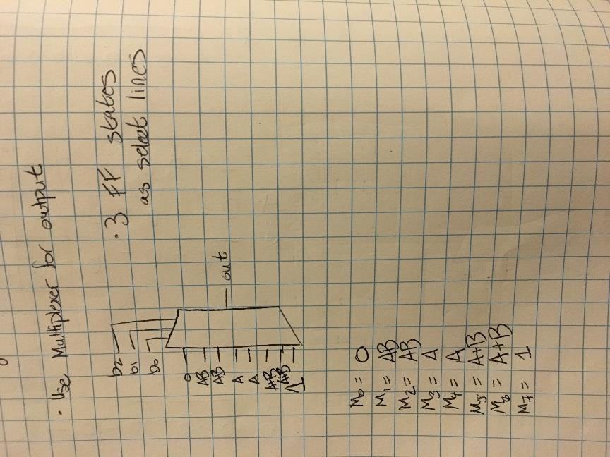
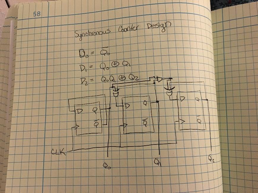
2 Purpose In this lab, a finite state machine was designed and fully implemented onto a protoboard utilizing 2 inputs to create a unique output sequence over a series of 8 clock cycles. The design was built and simulated using Altera Quartus 9.1. The utilization of this software enabled a simulation of the output waveform based on simulated inputs. With the confirmation of the design from the Quartus simulation, the design was implemented on a breadboard using the following ICs: 2 D Flip-Flops (74LS74), 1 AND (74LS08), 1 OR (74LS32), 1 XOR (74LS86), 1 8:1 Multiplexer (74LS151), and timer. Additionally, 4 resistors, 2 capacitors, and 1 8-pronged SPST switch. Finally, the finished design was tested using LogicPort software to ensure proper operation. The design constraints for the output can be seen in Figure 1. AB Z Figure 1 Procedure The original design for the finite state machine was initially created from the state transition diagram that can be seen in Figure 2 below. Our design utilized a Mealy Machine design to reduce the number of necessary states. This diagram was then utilized to create a state transition table to determine the next state based on inputs and previous states. This table can be seen in Figure 3 below. Using the state transition table, we designed a synchronous 3-bit counter to store states 0-7. This design uses D flip flops (74LS74 IC) and can be seen in Figure 4 below. In order to generate the output of the design, an 8:1 multiplexer was utilized that uses the flip flop states Q2-Q0 as select lines and combinational logic of inputs A and B for the MUX inputs. This design can be seen in Figure 5 below. The final design of the finite state machine utilizes 2 XOR gates, 2 AND gates, 1 OR gate, as well as 3 D flip-flops, timer, and 1 8:1 MUX. This design can be seen in Figure 6 below.


3 Figure 2 Figure 3 Figure 4 Figure 5

4 Figure 6 After completion of the design, the circuit was created using Altera Quartus 9.1 to analyze its behavior. The completed design can be seen in Figure 7 (see attached). The Quartus software includes a waveform simulation that can be used to see the output of the created circuit. Using the NodeFinder function, Quartus was able to take all of the input and output signals and translate them into the waveform simulation. This simulation allows for user inputted data for each of the inputs. For our design implementation, we utilized a high signal for both the preset and clear inputs combined with an oscillating square-wave input for the clock. After running the simulation, the output of the Q signals can be observed. Additionally, the output sequence for inputs A=0, B=0 can be seen in Figure 8 (see attached). Inputs A=1, B=1 are visible in Figure 9 (see attached). After verification of the circuit operation from the Quartus software, the design was physically implemented on the protoboard through the use of IC chips and wires. The finished circuit implementation can be seen in Figure 10 below. In order to test the functionality of the protoboard circuit, the oscilloscope was used to observe the output waveform of the finite state machine. The output of the circuit for inputs 00, 01, 10, and 11 can be seen in Figures 11, 12, 13, and 14, respectively.
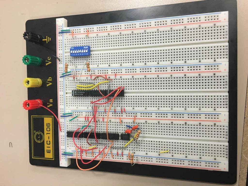
5 Figure 10


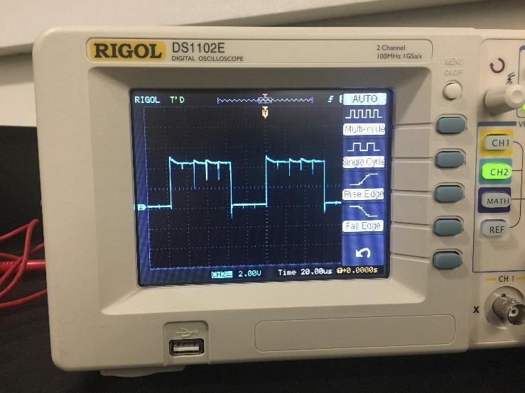
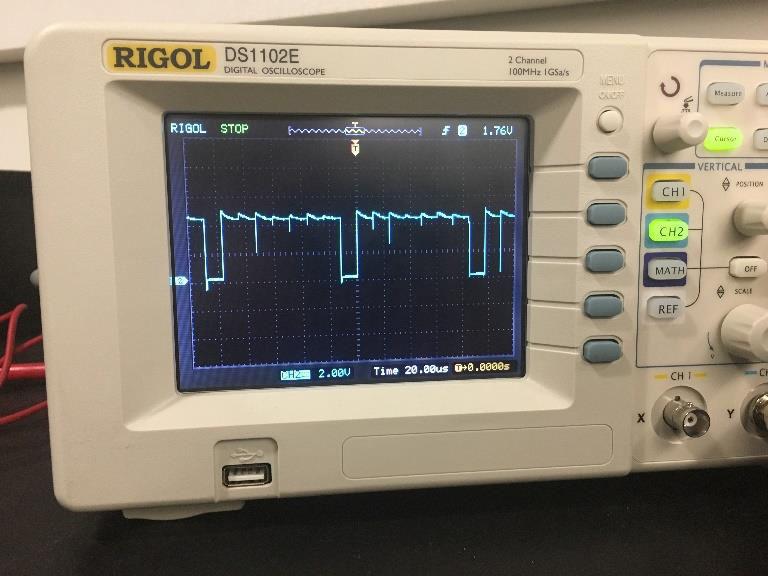
6 Figure 11 Figure 13 Figure 12 Figure 14
7 Finally, our design was tested using the LogicPort Logic Analyzer. This devices converts the analog signal of the circuit into a digital form of 0s and 1s. This tool enables effective observation of the circuit s inputs and outputs. In our testing, we connected the device to our clock as well as 6 inputs. Inputs D0-D5 were: input A, input B, Q0, Q1, Q2, and output. The generated waveforms for inputs 00, 01, 10, and 11 can be observed in Figures 15, 16, 17, and 18, respectively (see attached). Results The schematic of the design for the finite state machine can be seen in Figures 6 and 7. By using combinational logic, we were able to successfully create a 3-bit synchronous counter to store states 0-7. This was achieved using XOR gates with the lower bit Q value(s) as well as the previous Q state. For example, input D1 = Q0 Q1 and input D2 = Q0Q1 Q2. With each state stored in the flip-flops, the Q values can be used as the select lines for an 8:1 MUX to get the correct output for the specified state. Combinational logic of the inputs A and B were used to get inputs M0 M7 for the MUX. These inputs were 0, AB, AB, A, A, A+B, A+B, and 1, respectively. The 555 timer, as seen in Figure 19 below, was designed using a capacitance of 10.8 nf and a resistance of 500 Ω. This output timing was calculated using the equations from the ECE 501 Lab Manual. This device implementation led to a calculated period T was μ s. The output of this timing circuit was used as the input for the clocking signal of each D flip-flop. Figure 19
8 The Quartus implementation of the finite state machine verified the operation of the design, providing the necessary output waveform as specified in the design constraints. After physical implementation on the protoboard, both the oscilloscope and the LogicPort Logic Analyzer further verified proper operation of the circuit. As the inputs A and B increased from 00 to 11, the time high (th) of the output waveform increased as well. This can be seen in Figures for the oscilloscope and Figures 1518 for the Logic Analyzer. The resultant duty cycles of the output waveform for inputs 00, 01, 10, and 11 were ~ 12.5%, 37.5%, 62.5%, and 87.5%, respectively. These duty cycles are consistent with the expected outputs of the finite state machine. Conclusion Our original design (Figure 6) proved to be a successful implementation of the finite state machine. With the design constraint of the circuit switching to the proper output sequence at any point based on the inputs A and B, the design was greatly simplified to a Mealy Machine with only 8 states. These 8 states were stored using a 3bit synchronous counter, which shared a common clock from a 555 timer. The ability to use a MUX further simplified the design as the use of the Q states of the flip-flops as the select lines allowed for MUX inputs dependent only upon A and B. These inputs were implemented through the use of simple combinational logic. Both the oscilloscope and LogicPort Logic Analyzer verified proper operation of the finite state machine by providing the output waveform with the corresponding duty cycles. The use of circuit simulation software, specifically LogicPort, provided an effective and efficient technique of converting the analog signals of the circuit into digital waveforms for easy viewing. References 1. ECE 0501 Digital Systems Laboratory Custom Course Materials. Laboratory Notebook. University of Pittsburgh.
9
10
11
EE 307 Project #1 Whac-A-Mole
 EE 307 Project #1 Whac-A-Mole Performed 10/25/2008 to 11/04/2008 Report finished 11/09/2008 John Tooker Chenxi Liu Abstract: In this project, we made a digital circuit that operates Whac-A-Mole game. Quartus
Digital Electronics Course Objectives
 Digital Electronics Course Objectives In this course, we learning is reported using Standards Referenced Reporting (SRR). SRR seeks to provide students with grades that are consistent, are accurate, and
Lab Experiments. Boost converter (Experiment 2) Control circuit (Experiment 1) Power diode. + V g. C Power MOSFET. Load.
 Control circuit (Experiment 1) Power diode. + V g. C Power MOSFET. Load.") Lab Experiments L Power diode V g C Power MOSFET Load Boost converter (Experiment 2) V ref PWM chip UC3525A Gate driver TSC427 Control circuit (Experiment 1) Adjust duty cycle D The UC3525 PWM Control
Lab Experiments L Power diode V g C Power MOSFET Load Boost converter (Experiment 2) V ref PWM chip UC3525A Gate driver TSC427 Control circuit (Experiment 1) Adjust duty cycle D The UC3525 PWM Control
Digital Electronic Concepts
 Western Technical College 10662137 Digital Electronic Concepts Course Outcome Summary Course Information Description Career Cluster Instructional Level Total Credits 4.00 Total Hours 108.00 This course
DIGITAL ELECTRONICS: LOGIC AND CLOCKS
 DIGITL ELECTRONICS: LOGIC ND CLOCKS L 9 INTRO: INTRODUCTION TO DISCRETE DIGITL LOGIC, MEMORY, ND CLOCKS GOLS In this experiment, we will learn about the most basic elements of digital electronics, from
HIGH LOW Astable multivibrators HIGH LOW 1:1
 1. Multivibrators A multivibrator circuit oscillates between a HIGH state and a LOW state producing a continuous output. Astable multivibrators generally have an even 50% duty cycle, that is that 50% of
To design/build monostable multivibrators using 555 IC and verify their operation using measurements by observing waveforms.
 AIM: SUBJECT: ANALOG ELECTRONICS (2130902) EXPERIMENT NO. 09 DATE : TITLE: TO DESIGN/BUILD MONOSTABLE MULTIVIBRATORS USING 555 IC AND VERIFY THEIR OPERATION USING MEASUREMENTS BY OBSERVING WAVEFORMS. DOC.
Java Bread Board Introductory Digital Electronics Exercise 2, Page 1
 Java Bread Board Introductory Digital Electronics Exercise 2, Page 1 JBB Excercise 2 The aim of this lab is to demonstrate how basic logic gates can be used to implement simple memory functions, introduce
EXPERIMENT 12: DIGITAL LOGIC CIRCUITS
 EXPERIMENT 12: DIGITAL LOGIC CIRCUITS The purpose of this experiment is to gain some experience in the use of digital logic circuits. These circuits are used extensively in computers and all types of electronic
Digital Logic Circuits
 Digital Logic Circuits Let s look at the essential features of digital logic circuits, which are at the heart of digital computers. Learning Objectives Understand the concepts of analog and digital signals
Lab 12: Timing sequencer (Version 1.3)
") Lab 12: Timing sequencer (Version 1.3) WARNING: Use electrical test equipment with care! Always double-check connections before applying power. Look for short circuits, which can quickly destroy expensive
Lab 12: Timing sequencer (Version 1.3) WARNING: Use electrical test equipment with care! Always double-check connections before applying power. Look for short circuits, which can quickly destroy expensive
PRESENTATION OF THE PROJECTX-FINAL LEVEL 1.
 Implementation of digital it frequency dividersid PRESENTATION OF THE PROJECTX-FINAL LEVEL 1. Why frequency divider? Motivation widely used in daily life Time counting (electronic clocks, traffic lights,
Sequential Logic Circuits
 LAB EXERCISE - 5 Page 1 of 6 Exercise 5 Sequential Logic Circuits 1 - Introduction Goal of the exercise The goals of this exercise are: - verify the behavior of simple sequential logic circuits; - measure
DEPARTMENT OF ELECTRICAL ENGINEERING LAB WORK EE301 ELECTRONIC CIRCUITS
 DEPARTMENT OF ELECTRICAL ENGINEERING LAB WORK EE301 ELECTRONIC CIRCUITS EXPERIMENT : 4 TITLE : 555 TIMERS OUTCOME : Upon completion of this unit, the student should be able to: 1. gain experience with
Exercise 1: AND/NAND Logic Functions
 Exercise 1: AND/NAND Logic Functions EXERCISE OBJECTIVE When you have completed this exercise, you will be able to determine the operation of an AND and a NAND logic gate. You will verify your results
OBJECTIVE The purpose of this exercise is to design and build a pulse generator.
 ELEC 4 Experiment 8 Pulse Generators OBJECTIVE The purpose of this exercise is to design and build a pulse generator. EQUIPMENT AND PARTS REQUIRED Protoboard LM555 Timer, AR resistors, rated 5%, /4 W,
Digital Logic Troubleshooting
 Digital Logic Troubleshooting Troubleshooting Basic Equipment Circuit diagram Data book (for IC pin outs) Logic probe Voltmeter Oscilloscope Advanced Logic analyzer 1 Basic ideas Troubleshooting is systemic
ELECTROVATE. Electromania Problem Statement Discussion
 ELECTROVATE Electromania Problem Statement Discussion An Competition Basic Circuiting What is Electromania? Innovation Debugging Lets Revise the Basics Electronics Digital Analog Digital Electronics Similar
ICS 151 Final. (Last Name) (First Name)
 (First Name)") ICS 151 Final Name Student ID Signature :, (Last Name) (First Name) : : Instructions: 1. Please verify that your paper contains 19 pages including this cover and 3 blank pages. 2. Write down your Student-Id
ICS 151 Final Name Student ID Signature :, (Last Name) (First Name) : : Instructions: 1. Please verify that your paper contains 19 pages including this cover and 3 blank pages. 2. Write down your Student-Id
Solutions. ICS 151 Final. Q1 Q2 Q3 Q4 Total Credit Score. Instructions: Student ID. (Last Name) (First Name) Signature
 (First Name) Signature") ICS 151 Final Name Student ID Signature :, (Last Name) (First Name) : : Instructions: 1. Please verify that your paper contains 19 pages including this cover and 3 blank pages. 2. Write down your Student-Id
ICS 151 Final Name Student ID Signature :, (Last Name) (First Name) : : Instructions: 1. Please verify that your paper contains 19 pages including this cover and 3 blank pages. 2. Write down your Student-Id
Sequential Logic Circuits
 Exercise 2 Sequential Logic Circuits 1 - Introduction Goal of the exercise The goals of this exercise are: - verify the behavior of simple sequential logic circuits; - measure the dynamic parameters of
CPE 100L LOGIC DESIGN I
 CPE 100L LABORATORY 3: COMBINATIONAL CIRCUIT DESIGN FULL ADDER BY GRZEGORZ CHMAJ DEPARTMENT OF ELECTRICAL AND COMPUTER ENGINEERING UNIVERSITY OF NEVADA, LAS VEGAS GOALS: Develop the ability to write a
UMAINE ECE Morse Code ROM and Transmitter at ISM Band Frequency
 UMAINE ECE Morse Code ROM and Transmitter at ISM Band Frequency Jamie E. Reinhold December 15, 2011 Abstract The design, simulation and layout of a UMAINE ECE Morse code Read Only Memory and transmitter
INSTITUTE OF AERONAUTICAL ENGINEERING (Autonomous) Dundigal, Hyderabad
 Dundigal, Hyderabad") 1 P a g e INSTITUTE OF AERONAUTICAL ENGINEERING (Autonomous) Dundigal, Hyderabad - 500 043 ELECTRONICS AND COMMUNICATION ENGINEERING TUTORIAL QUESTION BANK Name : INTEGRATED CIRCUITS APPLICATIONS Code
1 P a g e INSTITUTE OF AERONAUTICAL ENGINEERING (Autonomous) Dundigal, Hyderabad - 500 043 ELECTRONICS AND COMMUNICATION ENGINEERING TUTORIAL QUESTION BANK Name : INTEGRATED CIRCUITS APPLICATIONS Code
CONTENTS Sl. No. Experiment Page No
 CONTENTS Sl. No. Experiment Page No 1a Given a 4-variable logic expression, simplify it using Entered Variable Map and realize the simplified logic expression using 8:1 multiplexer IC. 2a 3a 4a 5a 6a 1b
Experiment EB2: IC Multivibrator Circuits
 EEE1026 Electronics II: Experiment Instruction Learning Outcomes Experiment EB2: IC Multivibrator Circuits LO1: Explain the principles and operation of amplifiers and switching circuits LO2: Analyze high
t w = Continue to the next page, where you will draw a diagram of your design.
 Name EET 1131 Lab #13 Multivibrators OBJECTIVES: 1. To design and test a monostable multivibrator (one-shot) using a 555 IC. 2. To analyze and test an astable multivibrator (oscillator) using a 555 IC.
Exercise 2: OR/NOR Logic Functions
 Exercise 2: OR/NOR Logic Functions EXERCISE OBJECTIVE When you have completed this exercise, you will be able to determine the operation of an OR and a NOR logic gate. You will verify your results by generating
Class #6: Experiment The 555-Timer & Pulse Width Modulation
 Class #6: Experiment The 555-Timer & Pulse Width Modulation Purpose: In this experiment we look at the 555-timer, a device that uses digital devices and other electronic switching elements to generate
LABORATORY 6 v3 TIME DOMAIN
 University of California Berkeley Department of Electrical Engineering and Computer Sciences EECS 100, Professor Bernhard Boser LABORATORY 6 v3 TIME DOMAIN Inductors and capacitors add a host of new circuit
DEPARTMENT OF ELECTRICAL ENGINEERING AND COMPUTER SCIENCE MASSACHUSETTS INSTITUTE OF TECHNOLOGY CAMBRIDGE, MASSACHUSETTS 02139
 DEPARTMENT OF ELECTRICAL ENGINEERING AND COMPUTER SCIENCE MASSACHUSETTS INSTITUTE OF TECHNOLOGY CAMBRIDGE, MASSACHUSETTS 019.101 Introductory Analog Electronics Laboratory Laboratory No. READING ASSIGNMENT
Lab 7: DELTA AND SIGMA-DELTA A/D CONVERTERS
 ANALOG & TELECOMMUNICATION ELECTRONICS LABORATORY EXERCISE 6 Lab 7: DELTA AND SIGMA-DELTA A/D CONVERTERS Goal The goals of this experiment are: - Verify the operation of a differential ADC; - Find the
Lab 2 Revisited Exercise
 Lab 2 Revisited Exercise +15V 100k 1K 2N2222 Wire up led display Note the ground leads LED orientation 6.091 IAP 2008 Lecture 3 1 Comparator, Oscillator +5 +15 1k 2 V- 7 6 Vin 3 V+ 4 V o Notice that power
UNIVERSITY OF CALIFORNIA, DAVIS Department of Electrical and Computer Engineering. EEC 180A DIGITAL SYSTEMS I Winter 2015
 UNIVERSITY OF CALIFORNIA, DAVIS Department of Electrical and Computer Engineering EEC 180A DIGITAL SYSTEMS I Winter 2015 LAB 2: INTRODUCTION TO LAB INSTRUMENTS The purpose of this lab is to introduce the
ASTABLE MULTIVIBRATOR
 555 TIMER ASTABLE MULTIIBRATOR MONOSTABLE MULTIIBRATOR 555 TIMER PHYSICS (LAB MANUAL) PHYSICS (LAB MANUAL) 555 TIMER Introduction The 555 timer is an integrated circuit (chip) implementing a variety of
ENGINEERING TRIPOS PART II A ELECTRICAL AND INFORMATION ENGINEERING TEACHING LABORATORY EXPERIMENT 3B2-B DIGITAL INTEGRATED CIRCUITS
 ENGINEERING TRIPOS PART II A ELECTRICAL AND INFORMATION ENGINEERING TEACHING LABORATORY EXPERIMENT 3B2-B DIGITAL INTEGRATED CIRCUITS OBJECTIVES : 1. To interpret data sheets supplied by the manufacturers
PHYSICS 536 Experiment 14: Basic Logic Circuits
 PHYSICS 5 Experiment 4: Basic Logic Circuits Several T 2 L ICs will be used to illustrate basic logic functions. Their pin connections are shown in the following sketch, which is a top view. 4 2 9 8 +5V
PreLab 6 PWM Design for H-bridge Driver (due Oct 23)
") GOAL PreLab 6 PWM Design for H-bridge Driver (due Oct 23) The overall goal of Lab6 is to demonstrate a DC motor controller that can adjust speed and direction. You will design the PWM waveform and digital
GOAL PreLab 6 PWM Design for H-bridge Driver (due Oct 23) The overall goal of Lab6 is to demonstrate a DC motor controller that can adjust speed and direction. You will design the PWM waveform and digital
Code No: R Set No. 1
 Code No: R05310402 Set No. 1 1. (a) What are the parameters that are necessary to define the electrical characteristics of CMOS circuits? Mention the typical values of a CMOS NAND gate. (b) Design a CMOS
LABORATORY EXPERIMENT. Infrared Transmitter/Receiver
 LABORATORY EXPERIMENT Infrared Transmitter/Receiver (Note to Teaching Assistant: The week before this experiment is performed, place students into groups of two and assign each group a specific frequency
Verification of competency for ELTR courses
 Verification of competency for ELTR courses The purpose of these performance assessment activities is to verify the competence of a prospective transfer student with prior work experience and/or formal
ANALOG TO DIGITAL CONVERTER
 Final Project ANALOG TO DIGITAL CONVERTER As preparation for the laboratory, examine the final circuit diagram at the end of these notes and write a brief plan for the project, including a list of the
Department of Electronics & Communication Engineering LAB MANUAL SUBJECT: DIGITAL COMMUNICATION LABORATORY [ECE324] (Branch: ECE)
![Department of Electronics & Communication Engineering LAB MANUAL SUBJECT: DIGITAL COMMUNICATION LABORATORY [ECE324] (Branch: ECE)](/thumbs/96/127341232.jpg "Department of Electronics & Communication Engineering LAB MANUAL SUBJECT: DIGITAL COMMUNICATION LABORATORY [ECE324] (Branch: ECE)") Department of Electronics & Communication Engineering LAB MANUAL SUBJECT: DIGITAL COMMUNICATION LABORATORY [ECE324] B.Tech Year 3 rd, Semester - 5 th (Branch: ECE) Version: 01 st August 2018 The LNM Institute
Department of Electronics & Communication Engineering LAB MANUAL SUBJECT: DIGITAL COMMUNICATION LABORATORY [ECE324] B.Tech Year 3 rd, Semester - 5 th (Branch: ECE) Version: 01 st August 2018 The LNM Institute
Project Board Game Counter: Digital
 Project 1.3.3 Board Game Counter: Digital Introduction Just a few short weeks ago, most of you knew little or nothing about digital electronics. Now you are about to build and simulate a complete design.
EE2304 Implementation of a Stepper Motor using CMOS Devices Fall 2004 WEEK -2-
 WEEK -2-1. Objective Design a controller for a stepper motor that will be capable of: Making the motor rotate with variable speed (the user should be able to adjust the rotational speed easily and without
1.) If a 3 input NOR gate has eight input possibilities, how many of those possibilities result in a HIGH output? (a.) 1 (b.) 2 (c.) 3 (d.) 7 (e.
 If a 3 input NOR gate has eight input possibilities, how many of those possibilities result in a HIGH output? (a.) 1 (b.) 2 (c.) 3 (d.) 7 (e.") Name: Multiple Choice 1.) If a 3 input NOR gate has eight input possibilities, how many of those possibilities result in a HIGH output? (a.) 1 (b.) 2 (c.) 3 (d.) 7 (e.) 8 2.) The output of an OR gate with
Name: Multiple Choice 1.) If a 3 input NOR gate has eight input possibilities, how many of those possibilities result in a HIGH output? (a.) 1 (b.) 2 (c.) 3 (d.) 7 (e.) 8 2.) The output of an OR gate with
Electronic Instrumentation
 5V 1 1 1 2 9 10 7 CL CLK LD TE PE CO 15 + 6 5 4 3 P4 P3 P2 P1 Q4 Q3 Q2 Q1 11 12 13 14 2-14161 Electronic Instrumentation Experiment 7 Digital Logic Devices and the 555 Timer Part A: Basic Logic Gates Part
Exercise 1: EXCLUSIVE OR/NOR Gate Functions
 EXCLUSIVE-OR/NOR Gates Digital Logic Fundamentals Exercise 1: EXCLUSIVE OR/NOR Gate Functions EXERCISE OBJECTIVE When you have completed this exercise, you will be able to demonstrate the operation of
Lab 8: SWITCHED CAPACITOR CIRCUITS
 ANALOG & TELECOMMUNICATION ELECTRONICS LABORATORY EXERCISE 8 Lab 8: SWITCHED CAPACITOR CIRCUITS Goal The goals of this experiment are: - Verify the operation of basic switched capacitor cells, - Measure
University of North Carolina-Charlotte Department of Electrical and Computer Engineering ECGR 3157 Electrical Engineering Design II Fall 2013
 Exercise 1: PWM Modulator University of North Carolina-Charlotte Department of Electrical and Computer Engineering ECGR 3157 Electrical Engineering Design II Fall 2013 Lab 3: Power-System Components and
DC/AC CIRCUITS: CONVENTIONAL FLOW TEXTBOOKS
 4 PEARSON CUSTOM ELECTRONICS TECHNOLOGY DC/AC CIRCUITS: CONVENTIONAL FLOW TEXTBOOKS AVAILABLE MARCH 2009 Boylestad Introductory Circuit Analysis, 11/e, 0-13-173044-4 Introduction 32 LC4501 Voltage and
). The THRESHOLD works in exactly the opposite way; whenever the THRESHOLD input is above 2/3V CC
. The THRESHOLD works in exactly the opposite way; whenever the THRESHOLD input is above 2/3V CC") ENGR 210 Lab 8 RC Oscillators and Measurements Purpose: In the previous lab you measured the exponential response of RC circuits. Typically, the exponential time response of a circuit becomes important
ENGR 210 Lab 8 RC Oscillators and Measurements Purpose: In the previous lab you measured the exponential response of RC circuits. Typically, the exponential time response of a circuit becomes important
ENGR-4300 Fall 2006 Project 3 Project 3 Build a 555-Timer
 ENGR-43 Fall 26 Project 3 Project 3 Build a 555-Timer For this project, each team, (do this as team of 4,) will simulate and build an astable multivibrator. However, instead of using the 555 timer chip,
Laboratory Manual CS (P) Digital Systems Lab
 Digital Systems Lab") Laboratory Manual CS 09 408 (P) Digital Systems Lab INDEX CYCLE I A. Familiarization of digital ICs and digital IC trainer kit 1 Verification of truth tables B. Study of combinational circuits 2. Verification
Laboratory Manual CS 09 408 (P) Digital Systems Lab INDEX CYCLE I A. Familiarization of digital ICs and digital IC trainer kit 1 Verification of truth tables B. Study of combinational circuits 2. Verification
DEPARTMENT OF ELECTRICAL ENGINEERING AND COMPUTER SCIENCE MASSACHUSETTS INSTITUTE OF TECHNOLOGY CAMBRIDGE, MASSACHUSETTS 02139
 DEPARTMENT OF ELECTRICAL ENGINEERING AND COMPUTER SCIENCE MASSACHUSETTS INSTITUTE OF TECHNOLOGY CAMBRIDGE, MASSACHUSETTS 019 Spring Term 00.101 Introductory Analog Electronics Laboratory Laboratory No.
Lab Exercises. Exercise 1. Objective. Theory. Lab Exercises
 Lab Exercises Exercise 1 Objective! Study the generation of differential binary signal.! Study the differential PSK modulation.! Study the differential PSK demodulation. Lab Exercises Theory Carrier and
Lab# 13: Introduction to the Digital Logic
 Lab# 13: Introduction to the Digital Logic Revision: October 30, 2007 Print Name: Section: In this lab you will become familiar with Physical and Logical Truth tables. As well as asserted high, asserted
555 Timer and Its Application
 ANALOG ELECTRONICS (AE) 555 Timer and Its Application 1 Prepared by: BE-EE Amish J. Tankariya SEMESTER-III SUBJECT- ANALOG ELECTRONICS (AE) GTU Subject Code :- 210902 2 OBJECTIVES 555 timer; What is the
Electronics. RC Filter, DC Supply, and 555
 Electronics RC Filter, DC Supply, and 555 0.1 Lab Ticket Each individual will write up his or her own Lab Report for this two-week experiment. You must also submit Lab Tickets individually. You are expected
Module -18 Flip flops
 1 Module -18 Flip flops 1. Introduction 2. Comparison of latches and flip flops. 3. Clock the trigger signal 4. Flip flops 4.1. Level triggered flip flops SR, D and JK flip flops 4.2. Edge triggered flip
TTL LOGIC and RING OSCILLATOR TTL
 ECE 2274 TTL LOGIC and RING OSCILLATOR TTL We will examine two digital logic inverters. The first will have a passive resistor pull-up output stage. The second will have an active transistor and current
EE-110 Introduction to Engineering & Laboratory Experience Saeid Rahimi, Ph.D. Lab Timer: Blinking LED Lights and Pulse Generator
 EE-110 Introduction to Engineering & Laboratory Experience Saeid Rahimi, Ph.D. Lab 9 555 Timer: Blinking LED Lights and Pulse Generator In many digital and analog circuits it is necessary to create a clock
First Optional Homework Problem Set for Engineering 1630, Fall 2014
 First Optional Homework Problem Set for Engineering 1630, Fall 014 1. Using a K-map, minimize the expression: OUT CD CD CD CD CD CD How many non-essential primes are there in the K-map? How many included
Practical Workbook Logic Design & Switching Theory
 Practical Workbook Logic Design & Switching Theory Name : Year : Batch : Roll No : Department: Second Edition Fall 2017-18 Dept. of Computer & Information Systems Engineering NED University of Engineering
Number of Lessons:155 #14B (P) Electronics Technology with Digital and Microprocessor Laboratory Completion Time: 42 months
 Electronics Technology with Digital and Microprocessor Laboratory Completion Time: 42 months") PROGRESS RECORD Study your lessons in the order listed below. Number of Lessons:155 #14B (P) Electronics Technology with Digital and Microprocessor Laboratory Completion Time: 42 months 1 2330A Current
PROGRESS RECORD Study your lessons in the order listed below. Number of Lessons:155 #14B (P) Electronics Technology with Digital and Microprocessor Laboratory Completion Time: 42 months 1 2330A Current
Digital Electronics. A. I can list five basic safety rules for electronics. B. I can properly display large and small numbers in proper notation,
 St. Michael Albertville High School Teacher: Scott Danielson September 2016 Content Skills Learning Targets Standards Assessment Resources & Technology CEQ: WHAT MAKES DIGITAL ELECTRONICS SO IMPORTANT
ENG 100 Electric Circuits and Systems Lab 6: Introduction to Logic Circuits
 ENG 100 Electric Circuits and Systems Lab 6: Introduction to Logic Circuits Professor P. Hurst Lecture 5:10p 6:00p TR, Kleiber Hall Lab 2:10p 5:00p F, 2161 Kemper Hall LM741 Operational Amplifier Courtesy
University of California at Berkeley Donald A. Glaser Physics 111A Instrumentation Laboratory
 Published on Instrumentation LAB (http://instrumentationlab.berkeley.edu) Home > Lab Assignments > Digital Labs > Digital Circuits II Digital Circuits II Submitted by Nate.Physics on Tue, 07/08/2014-13:57
Geared Oscillator Project Final Design Review. Nick Edwards Richard Wright
 Geared Oscillator Project Final Design Review Nick Edwards Richard Wright This paper outlines the implementation and results of a variable-rate oscillating clock supply. The circuit is designed using a
High Group Hz Hz. 697 Hz A. 770 Hz B. 852 Hz C. 941 Hz * 0 # D. Table 1. DTMF Frequencies
 AN-1204 DTMF Tone Generator Dual-tone multi-frequency signaling (DTMF) was first developed by Bell Labs in the 1950 s as a method to support the then revolutionary push button phone. This signaling system
Name: First-Order Response: RC Networks Objective: To gain experience with first-order response of RC circuits
 First-Order Response: RC Networks Objective: To gain experience with first-order response of RC circuits Table of Contents: Pre-Lab Assignment 2 Background 2 National Instruments MyDAQ 2 Resistors 3 Capacitors
COMPUTER ORGANIZATION & ARCHITECTURE DIGITAL LOGIC CSCD211- DEPARTMENT OF COMPUTER SCIENCE, UNIVERSITY OF GHANA
 COMPUTER ORGANIZATION & ARCHITECTURE DIGITAL LOGIC LOGIC Logic is a branch of math that tries to look at problems in terms of being either true or false. It will use a set of statements to derive new true
CHAPTER 5 NOVEL CARRIER FUNCTION FOR FUNDAMENTAL FORTIFICATION IN VSI
 98 CHAPTER 5 NOVEL CARRIER FUNCTION FOR FUNDAMENTAL FORTIFICATION IN VSI 5.1 INTRODUCTION This chapter deals with the design and development of FPGA based PWM generation with the focus on to improve the
ECEN 720 High-Speed Links: Circuits and Systems. Lab3 Transmitter Circuits. Objective. Introduction. Transmitter Automatic Termination Adjustment
 1 ECEN 720 High-Speed Links: Circuits and Systems Lab3 Transmitter Circuits Objective To learn fundamentals of transmitter and receiver circuits. Introduction Transmitters are used to pass data stream
Time: 3 hours Max. Marks: 70 Answer any FIVE questions All questions carry equal marks
 Code: 9A02401 PRINCIPLES OF ELECTRICAL ENGINEERING (Common to EIE, E.Con.E, ECE & ECC) Time: 3 hours Max. Marks: 70 1 In a series RLC circuit, R = 5 Ω, L = 1 H and C = 1 F. A dc v ltage f 20 V is applied
3.1 There are three basic logic functions from which all circuits can be designed: NOT (invert), OR, and
, OR, and") EE 2449 Experiment 3 Jack Levine and Nancy Warter-Perez, Revised 6/12/17 CALIFORNIA STATE UNIVERSITY LOS ANGELES Department of Electrical and Computer Engineering EE-2449 Digital Logic Lab EXPERIMENT 3
EE 2449 Experiment 3 Jack Levine and Nancy Warter-Perez, Revised 6/12/17 CALIFORNIA STATE UNIVERSITY LOS ANGELES Department of Electrical and Computer Engineering EE-2449 Digital Logic Lab EXPERIMENT 3
Theory: The idea of this oscillator comes from the idea of positive feedback, which is described by Figure 6.1. Figure 6.1: Positive Feedback
 Name1 Name2 12/2/10 ESE 319 Lab 6: Colpitts Oscillator Introduction: This lab introduced the concept of feedback in combination with bipolar junction transistors. The goal of this lab was to first create
VCC. Digital 16 Frequency Divider Digital-to-Analog Converter Butterworth Active Filter Sample-and-Hold Amplifier (part 2) Last Update: 03/19/14
 Last Update: 03/19/14") Digital 16 Frequency Divider Digital-to-Analog Converter Butterworth Active Filter Sample-and-Hold Amplifier (part 2) ECE3204 Lab 5 Objective The purpose of this lab is to design and test an active Butterworth
Digital 16 Frequency Divider Digital-to-Analog Converter Butterworth Active Filter Sample-and-Hold Amplifier (part 2) ECE3204 Lab 5 Objective The purpose of this lab is to design and test an active Butterworth
555 Timer/Oscillator Circuits
 Page 1 of 5 Laboratory Goals Familiarize students with the 555 IC and its uses Design a free-running oscillator Design a triggered one-shot circuit Compare actual to theoretical values for the circuits
Draw in the space below a possible arrangement for the resistor and capacitor. encapsulated components
 1). An encapsulated component is known to consist of a resistor and a capacitor. It has two input terminals and two output terminals. A 5V, 1kHz square wave signal is connected to the input terminals and
Basic Logic Circuits
 Basic Logic Circuits Required knowledge Measurement of static characteristics of nonlinear circuits. Measurement of current consumption. Measurement of dynamic properties of electrical circuits. Definitions
Dedan Kimathi University of technology. Department of Electrical and Electronic Engineering. EEE2406: Instrumentation. Lab 2
 Dedan Kimathi University of technology Department of Electrical and Electronic Engineering EEE2406: Instrumentation Lab 2 Title: Analogue to Digital Conversion October 2, 2015 1 Analogue to Digital Conversion
UNIT II: Clocked Synchronous Sequential Circuits. CpE 411 Advanced Logic Circuits Design 1
 UNIT II: Clocked Synchronous Sequential Circuits CpE 411 Advanced Logic Circuits Design 1 Unit Outline Analysis of Sequential Circuits State Tables State Diagrams Flip-flop Excitation Tables Basic Design
Breadboard Primer. Experience. Objective. No previous electronics experience is required.
 Breadboard Primer Experience No previous electronics experience is required. Figure 1: Breadboard drawing made using an open-source tool from fritzing.org Objective A solderless breadboard (or protoboard)
EE283 Electrical Measurement Laboratory Laboratory Exercise #7: Digital Counter
 EE283 Electrical Measurement Laboratory Laboratory Exercise #7: al Counter Objectives: 1. To familiarize students with sequential digital circuits. 2. To show how digital devices can be used for measurement
Lecture 7 ECEN 4517/5517
 Lecture 7 ECEN 4517/5517 Experiments 4-5: inverter system Exp. 4: Step-up dc-dc converter (cascaded boost converters) Analog PWM and feedback controller to regulate HVDC Exp. 5: DC-AC inverter (H-bridge)
15EI205L-ANALOG AND DIGITAL INTEGRATED CIRCUITS LABORATORY MANUAL
 15EI205L-ANALOG AND DIGITAL INTEGRATED CIRCUITS LABORATORY MANUAL Department of Electronics and Instrumentation Engineering Faculty of Engineering and Technology Department of Electronics and Instrumentation
EECE 143 Lecture 0: Intro to Digital Laboratory
 EECE 143 Lecture 0: Intro to Digital Laboratory Syllabus * Class Notes Laboratory Equipment Experiment 0 * Experiment 1 Introduction Instructor Information: Mr. J. Christopher Perez Room: Haggerty Engineering,
ECE 261 CMOS VLSI Design Methodologies. Final Project Report. Vending Machine. Dec 13, 2007
 ECE 261 CMOS VLSI Design Methodologies Final Project Report Vending Machine Yuling Zhang Zhe Chen Yayuan Zhang Yanni Zhang Dec 13, 2007 Abstract This report gives the architectural design of a Vending
Experiment # 1 Introduction to Lab Equipment
 Experiment # 1 Introduction to Lab Equipment 1. Synopsis: In this introductory lab, we will review the basic concepts of digital logic design and learn how to use the equipment available in the laboratory.
DEGREE: BACHELOR IN INDUSTRIAL ELECTRONICS AND AUTOMATION YEAR: 2ND TERM: 2ND
 SESSION WEEK COURSE: ELECTRONICS ENGINEERING FUNDAMENTALS DEGREE: BACHELOR IN INDUSTRIAL ELECTRONICS AND AUTOMATION YEAR: 2ND TERM: 2ND The course has 29 sessions distributed during 15 weeks. The duration
University of Pittsburgh
 University of Pittsburgh Experiment #7 Lab Report Analog-Digital Applications Submission Date: 08/01/2018 Instructors: Dr. Ahmed Dallal Shangqian Gao Submitted By: Nick Haver & Alex Williams Station #2
Entry Level Assessment Blueprint Electronics Technology
 Blueprint Test Code: 4135 / Version: 01 Specific Competencies and Skills Tested in this Assessment: Safety Practices Demonstrate safe working procedures Explain the purpose of OSHA and how it promotes
Lab 5. Binary Counter
 Lab. Binary Counter Overview of this Session In this laboratory, you will learn: Continue to use the scope to characterize frequencies How to count in binary How to use an MC counter Introduction The TA
DIGITAL TO ANALOG AND ANALOG TO DIGITAL CONVERTER
 NLOG & TELECOMMUNICTION ELECTONICS LOTOY EXECISE 5 Lab 6: DIGITL TO NLOG ND NLOG TO DIGITL CONVETE Goal nalyze the behavior of a 6-bit D/ converter. Evaluate linear and nonlinear errors, nonmonotonicy
State Machine Oscillators
 by Kenneth A. Kuhn March 22, 2009, rev. March 31, 2013 Introduction State machine oscillators are based on periodic charging and discharging a capacitor to specific voltages using one or more voltage comparators
Real Analog - Circuits 1 Chapter 11: Lab Projects
 .3.4: Signal Conditioning Audio Application eal Analog Circuits Chapter : Lab Projects Overview: When making timevarying measurements, the sensor being used often has at least a few undesirable characteristics.
ENEE307 Lab 7 MOS Transistors 2: Small Signal Amplifiers and Digital Circuits
 ENEE307 Lab 7 MOS Transistors 2: Small Signal Amplifiers and Digital Circuits In this lab, we will be looking at ac signals with MOSFET circuits and digital electronics. The experiments will be performed
Lab 6. Binary Counter
 Lab 6. Binary Counter Overview of this Session In this laboratory, you will learn: Continue to use the scope to characterize frequencies How to count in binary How to use an MC14161 or CD40161BE counter
ENGR 210 Lab 12: Analog to Digital Conversion
 ENGR 210 Lab 12: Analog to Digital Conversion In this lab you will investigate the operation and quantization effects of an A/D and D/A converter. A. BACKGROUND 1. LED Displays We have been using LEDs