Nonlinear Characterization and Modeling Through Pulsed IV/S-Parameters
|
|
|
- Donna Hancock
- 5 years ago
- Views:
Transcription

1 Nonlinear Characterization and Modeling Through Pulsed IV/S-Parameters
2 OUTLINE Introduction Core device model extraction Model Enhancement Model Validation
3 Types of Large-Signal Transistor Models Convergence Operating range Physic model Compact model Behavioral model Extrapolation Accuracy Physical insight Easy modeling process Usability for Circuit design
4 Commercial compact FET models Mostly used models for GaN HEMTs FET models Number of parameters Electro-thermal effect Trapping Effects Original Device Context Curtice3 [1] 59 No No GaAs FET CFET [2] 53 Yes No HEMT EEHEMT1 [3] 71 No No HEMT Angelov [4] 80 Yes No HEMT/MESFET AMCAD HEMT1 [5] 65 Yes Yes GaN HEMT AMCAD GaN HEMT1 is the only model here with a complete extraction flow based on pulsed IV/RF measurements
5 Rs, Rd Idss Compact FET model extraction flow Rd y = x Rs 0.8 y = x T C y = x T C Small-Signal IV Model Non-linear capacitances Thermal model Trapping effects Rg Lg Cpg Ls Cpd Ld Rs Rd Ri Cds τ Gm Gd Cgs Cgd Rgd Dgs=f(Vgs) Dgd=f(Vgd) Ids=f(Vgs,Vds) Cgs=f(Vgs) Cgd=f(Vgd) Dgs=f(Vgs,T) Dgd=f(Vgd,T) Ids=f(Vgs,Vds,T) Rs=f(T) Rd=f(T) Ids=f(Vgs_trap,Vds,T) Various effects are successively added
6 Parameter extraction methodology
7 OUTLINE Introduction Core device model extraction Model Enhancement Model Validation

8 Parameter extraction methodology Core device model Pulsed IV / S parameter Measurements 1 st step: bias-dependant S parameters Multibias set of linear models 2 nd step: large signal fitting Modeling Nonlinear model
9 Parameter extraction methodology Core device model Pulsed IV / S parameter Measurements 1 st step: bias-dependant S parameters Multibias set of linear models 2 nd step: large signal fitting Modeling Nonlinear model


10 Pulsed IV measurements Short pulse : Quasi-isothermal conditions Low duty cycle : Constant mean temperature Quiescent bias point : Thermal conditions fixed Several quiescent bias point

11 Compact FET model extraction flow Small-Signal Modelling Process Pulsed S parameter measurements Rg Lg Cpg Ls Cpd Ld Rs Rd Ri Cds τ Gm Gd Cgs Cgd Rgd Bias Bias


12 Pulsed S parameter measurements The first & most important point : Pulsed S parameter measurements must not be noisy Small S2P measurement variation = strong influence over the linear model extraction : optimization algorithm Requirements : IVCAD Dynamic range in pulsed mode > 90dB for Duty Cycle ~ 5%
13 Pulsed S-parameter Measurements Pulsed S-parameter measurements must not be noisy at low duty cycle with narrow pulse width Pulse detection methods Wideband detection Narrowband detection Receiver samples IF filter Receiver samples IF filter No pulse desensitization Increased noise with narrow pulse width due to wider IF bandwidth Limited pulse width by maximum available IF bandwidth Narrower minimum pulse width than wideband pulse Reduced dynamic range with low duty cycle due to pulse desensitization by 20*log(duty cycle)
 10 us (150 khz) 5 us (280 khz) 1 us (1.5 MHz) 500 ns (3 MHz) Averaging 20 times in calibration and measurements 0.005 db 0.006 db 0.012 db 0.")
14 PNA/PNA-X Noise reduction techniques and performances Peak-to-peak noise with wideband detection at 10% duty cycle No averaging in calibration and measurements 0.03 db 0.04 db 0.06 db 0.09 db Pulse width (IFBW) 10 us (150 khz) 5 us (280 khz) 1 us (1.5 MHz) 500 ns (3 MHz) Averaging 20 times in calibration and measurements db db db db


15 PNA/PNA-X Noise reduction techniques and performances Dynamic range with wideband detection at 10% duty cycle with 10 us, 5 us, 1 us, 500 ns pulse width No averaging in calibration and measurements, 1% smoothing on Averaging 20 times in calibration and measurements, 1% smoothing on

16 PNA/PNA-X Noise reduction techniques and performances Peak-to-peak noise at 10% duty cycle Wideband detection with 20 times averaging in calibration and measurements Narrowband detection with no averaging in calibration and measurements Pulse width db db db db 10 us 5 us 1 us 500 ns db db db db
17 PNA/PNA-X Noise reduction techniques and performances Dynamic range with narrowband detection at 500 ns pulse width Hardware gating No Averaging, 1% smoothing on, 500 Hz IF bandwidth Crystal filter Software gating >100 db at 10% >100 db at 5% 90 db at 1% 85 db at 0.5% Spectral nulling
18 E836x Legacy PNA N524xA PNA-X N522xA New PNA Pulse generator External Internal/External Internal/External Pulse modulator External Internal/External Internal/External Wideband detection Max BW/Min PW 35 khz / 50 us 15 MHz / 100 ns 15 MHz / 100 ns High level noise* dbrms dbrms to dbrms Dynamic range** 114 to 123 db 124 to 129 db 127 db Narrowband detection Min IF gate width 20 ns <20 ns <20 ns Dynamic range*** 85 db <105 db <105 db * Specified as trace noise magnitude, at 20 GHz, at 1 khz IF bandwidth ** Specified performance at 20 GHz, at 10 Hz IF bandwidth *** Measured performance at 10 GHz at 10 Hz IF bandwidth, 1% duty cycle


 Dgd=f(Vgd)")
19 Compact FET model extraction flow Small-Signal IV Model Rg Lg Cpg Ls Cpd Ld Rs Rd Ri Cds τ Gm Gd Cgs Cgd Rgd Dgs=f(Vgs) Dgd=f(Vgd) Ids=f(Vgs,Vds) RF DC DC RF


20 Pulsed IV parameter measurements Pulsed IV measurements must be accurate from low to high voltage/current values Accurate IV data = Reliable current source Transconductance Leakage current Ideality factor schottky diode IVCAD


21 How to get accurate pulsed IV measurements? PIV system Pulsed IV parameter measurements
22 Pulsed IV parameter measurements How to get accurate pulsed IV measurements? +15V Gate 15 bits + sign Drain 250V 16 bits 15 bits + sign -15V 25V 16 bits Pulse shape monitoring 20ns time resolution
23 Pulsed IV parameter measurements How to get accurate pulsed IV measurements? 200mA 9µA 400µA 200mA 20mA 0mA 1µA 40µA 20mA -15V 0,6mV 65mV 15V 0V Measurement Resolution Voltage Absolute Accuracy Voltage Range

24 How to get accurate pulsed IV measurements? 10A Pulsed IV parameter measurements 200µA 20mA 1A 0A 22µA 2mA Measurement Resolution Voltage Absolute Accuracy Voltage Range 0,53mV 4,9mV 50mV 500mV 0V 25V 250V

25 Pulsed IV & S parameter measurements How to get accurate pulsed IV measurements? Synchronisation between Pulse IV and pulse S parameters


26 Pulsed S parameter measurements How to get accurate pulsed IV measurements? Synchronisation between Pulse IV and pulse S parameters
27 Parameter extraction methodology Core device model Pulsed IV / S parameter Measurements 1 st step: bias-dependant S parameters Multibias set of linear models 2 nd step: large signal fitting Modeling Nonlinear model
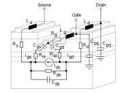
28 ignal model presents Small signal FET modeling circuit c circuit related to the ments Cpg Extrinsic parameters - pad capacitances Cpg, Cpd - port metallisation inductances Lg, Ld, Ls - port ohmic resistances Rg, Rd, Rs developped at the allows to optimize the ments in order to get ameters that do not he frequency Intrinsic parameters - channel capacitances Cgs, Cgd - voltage-controlled current source with transconductance gm and transit time delay tau - ohmic resistances Ri, Rgd - output capacitance Cds and resistance Rds G Lg Rg Rd Ld Transistor intrinsic intrinsèque transistor Cpd Rs Ls S Grille Gate Cgd Cgs Ri Transistor intrinsic intrinsèque transistor D Rgd Gm Source Drain Rds Cds Gm = Gm 0 e -j

![device is extracted from measured [S] parameters No Set min. and max.](/docs-images/80/82255518/images/29-2.jpg "for each extrinsic parameter - user choice - initiated by cold FET meas.")
29 Small signal FET modeling Extraction of extrinsic and intrinsic parameters: There is only one set of extrinsic parameters for which intrinsic parameters are independent from the frequency For a given set of extrinsic parameters, intrinsic admittance matrix of the device is extracted from measured [S] parameters No Set min. and max. for each extrinsic parameter - user choice - initiated by cold FET meas. Optimization algorithm: annealing, fast simulated diffusion (intrinsic parameters calculus) Fit? Yes Multi-biasing extraction of the linear model
30 OUTLINE Introduction Core device model extraction Model Enhancement Model Validation
31 Parameter extraction methodology Core device model Pulsed IV / S parameter measurement results 1 st step: bias-dependant S parameters Multibias set of linear models 2 nd step: large signal fitting Nonlinear model Model Enhancement Specific measurements - diodes - g-d breakdown - thermal effects - charge carrier trapping 3 rd step: setting of additional parameters Enhanced Nonlinear model
32 Rs, Rd Idss Compact FET model extraction flow Rd y = x Rs 0.8 y = x T C y = x T C Small-Signal IV Model Non-linear capacitances Thermal model Trapping effects Rg Lg Cpg Ls Cpd Ld Rs Rd Ri Cds τ Gm Gd Cgs Cgd Rgd Dgs=f(Vgs) Dgd=f(Vgd) Ids=f(Vgs,Vds) Cgs=f(Vgs) Cgd=f(Vgd) Dgs=f(Vgs,T) Dgd=f(Vgd,T) Ids=f(Vgs,Vds,T) Rs=f(T) Rd=f(T) Ids=f(Vgs_trap,Vds,T) Various effects are successively added
33 Non linear capacitances Gate charge is partitioned into gate source and gate-drain charge. Each charge expression is a function of both VDS and VGS. For power amplifier applications, 2D models do not bring a breakthrough in the precision, but they are much more complex 1 dimension capacitances extracted along optimal load-line are preferred due to simplicity. 1D capacitances with equations based on hyperbolic tangents are naturally charge conservatives Output Capacitance Cds is linear no voltage dependence (weak anyway) Cgd=f(Vgd) Cgs=f(Vgs) + Modeling simplicity. Very good convergence - Validity of the 1D? 33

34 Capacitances modeling: 1D vs 2D Non linear capacitances Better fit of the 2D model in wider domain But the 1D model has a good behavior 34
35 Non linear capacitances Cgd Feedback capacitance Cgd is a strong function of drain voltage. Cgd capacitance extracted along optimal load-line for power amplification
36 Non linear capacitances Cgs Input capacitance Cgs is a strong function of gate voltage. The gate-voltage non-linearity also effects model s harmonic generation Cgs capacitance extracted along optimal load-line for power amplification
 AMCAD drain current model formulation allows to predict very accurately the I-V curves, the partial derivatives gm and gd, the knee voltage and the")
37 Gm (S) Id (A) Output current source meas. model Vds (V) AMCAD drain current model formulation allows to predict very accurately the I-V curves, the partial derivatives gm and gd, the knee voltage and the transconductance decrease at high current Vgs (V)

38 Output current source Idss amplitude Vdsp, A slope P gd M, P fitting parameters Vp0 pinch-off AlphaGm, Vgm, BetaGm, Vdm gm (derivative)
39 Diodes Gate-drain and gate-source diode equations include forward conduction of gate current ID Is. e Alpha.Vd (a classical formulatio n)
40 Ids (ma) Igs (ma) Breakdown generator Gate-drain Breakdown generator The breakdown phenomena leads to a current from the drain to the gate when the device is pinched-off and for high values of Vds voltage. In this case, the whole 800 negative current characterized on the gate is seen in positive on the drain Vds (V) Vds (V) A polynomial expression with order 4 is necessary to model the cross of breakdown curves, with varies depending on the process
 1.0 0.8 0.6 0.4 0.2-0.0-0.2 Static 25 C 0 5 10 15 20 25 30 35 40 45 Vds (V) 0.5 0.4 0.3 0.2 0.1 0.0-0.1 1 150 C 0 5 10 15 20 25 30 35 40 45 Vds (V) 0.6 0.4 2 Dynamic 0.")
41 Ids (A) Ids (A) Ids (A) Ids (A) Static and Dynamic self-heating effects Thermal effects Temperature dependence with ambient or chuck temperature C Vds (V) Static 25 C Vds (V) C Vds (V) Dynamic Vds (V)

42 Thermal effects


43 Thermal effects Thermal impedance extraction by simulation


44 Thermal effects Thermal impedance extraction by measurements
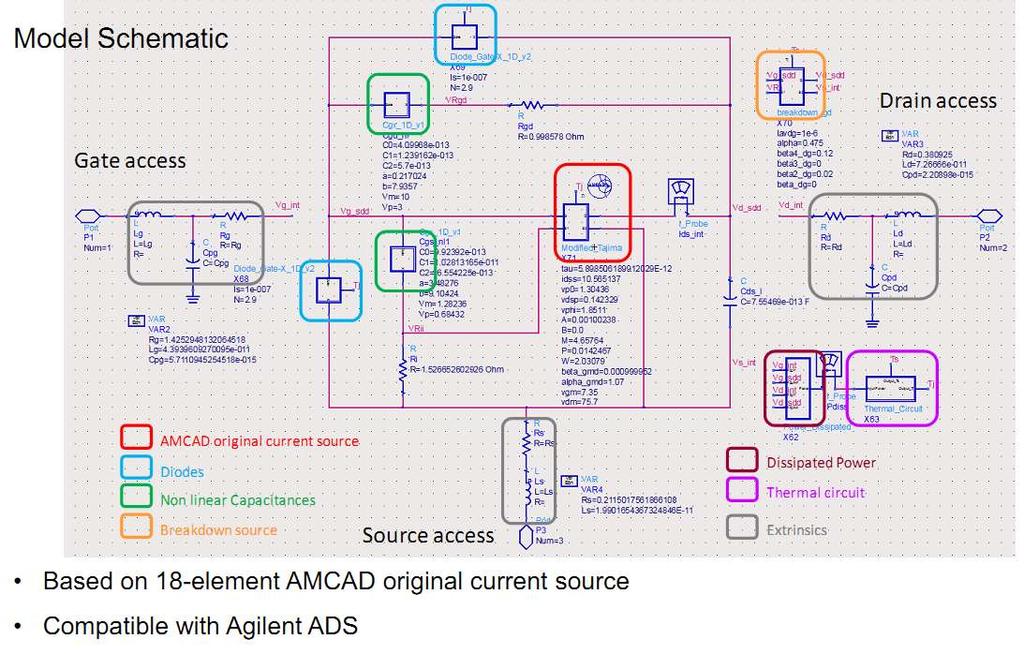
45 Thermal effects Drain current is only temperature dependent model element Takes into account ambient temperature and self-heating effects Thermal analog circuit to model self-heating and elevated heat sink temperatures Gate access Drain access RC cells AMCAD original current source Diodes Non linear Capacitances Breakdown source Source access Dissipated Power Thermal circuit Extrinsics
46 Vgs_int Trapping effects Charging and discharging of traps has influence Lg Rg on Ids and leads to current collapse. This is Cgd Rgd described in the model by trapping effects modifying the gate command and separated into gate and drain lag sub-circuits Cpg Vgs Vds Ibk Igd(T ) Gate access Drain access Cgs Igs(T ) Gate- & Drain-lag Ri AMCAD original current source Diodes Non linear Capacitances Breakdown source Source access Dissipated Power Thermal circuit Extrinsics Transistor intrinsèque Rs(T ) Ls

47 Trapping effects
48 Charge of the capacitance = Ionized traps Trapping effects Charge through Rcapture, Emission through Rémission R Rcapture Diode diode C C8 signal reshaping circuit Port Vout Port Vin R Remission Diode = dissymmetry of the capture and emission process Tuning of the magnitude of the trapping effects Fundamental assumption : dissymetry of the capture and emission process
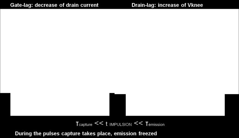
49 Ids (A) (H) Trapping effects Bias dependant gate lag -> current reduction over the entire characteristic Bias dependent drain lag -> current reduction and shifts the knee-voltage to a higher Vds Model covers knee walkout to avoid errors in calculation of output power gate-lag : Id => Pout H 0.4 drain-lag : Id Vknee => Pout Vds (V)
50 Ids (A) (H) Ids (A) (H) (H) Ids Ids (A) (A) (H) (H) (H) Ids (A) Pout W (H) Pout W (H) (H) Pout Pout Pout W W (H) (W) (H) (H) Trapping effects Decreasing form of the mean output current only reproduced with traps modeled meas model without traps model model with traps model H Pout H 0.25 Ids Pin( dbm) 22 meas 11 model without traps model model with traps model Pin (W)
51 OUTLINE Introduction Core device model extraction Model Enhancement Model Validation
52 Parameter extraction methodology Core device model Pulsed IV / S parameter measurement results Model Enhancement Specific measurements Model Validation Power measurements 1 st step: bias-dependant S parameters Multibias set of linear models 2 nd step: large signal fitting - diodes - g-d breakdown - thermal effects - charge carrier trapping 3 rd step: setting of additional parameters 4 th step: implementation in commercial simulator -load-pull measurements CW, pulsed 2-tones time domain 5 th step: validation and refinement Nonlinear model Enhanced Nonlinear model Final Nonlinear model
53 Pout (dbm) and Gain (db) Pout (dbm) and Gain (db) Large-signal Model validation Model validation of a 8x75 µm GaN HEMT with load-pull measurements performed at 6 GHz for optimum PAE load impedance in class-ab Model validation of a 8x400 µm GaN HEMT with load-pull measurements performed at 3 GHz for the optimum Pout load impedance in class-b meas. model Pout PAE gain PAE (%) meas. model Pout gain PAE PAE (%) Pin dbm Pin dbm -20
54 Model validation VNA Based load pull system is preferred for model validation Specific Architecture DC or pulse DC supplies + meas Units PA Gate T Low loss directional couplers DUT Drain T 50 Tuner f0 VNA Tuner f0, 2f0, 3f0 CW or pulse RF signal f0 or f1+f2
55 Model validation VNA Based load pull system is preferred for model validation

56 Power meter based system are wideband measurement system f0 2.f0 3.f0 VNA based system can be narrowband measurement system f0 f0 f0 2.f0 3.f0 2.f0 3.f0 2.f0 3.f0 More information for model validation or efficient design
57 VNA based Load Pull systems Some Measurement definition P_in: Power delivered to the DUT by the source P_out: Power delivered to the load impedance Power gain is the ratio of the power delivered to the load (P out ) to the power delivered to the transistor by the source (P in ).


58 Model validation VNA Based load pull system is preferred for model validation Specific Architecture DC or pulse DC supplies + meas Units PA Gate T Low loss directional couplers DUT Drain T 50 Tuner f0 VNA Tuner f0, 2f0, 3f0 CW or pulse RF signal f0 or f1+f2 Phase reference


59 Large signal impact - class AB, 25V, 10 GHz Comparison with measurements With non optimal loads : Time domain load pull measurements Deembedding in the intrinsic reference plane Parasitic extrinsic elements must be accurately extracted by previous S parameter measurements
60 Testing Model Validity with Pulsed IV Simulations (Using Agilent ADS) Is your FET model suitable for high-frequency design? Is dynamic behavior included? Is it well-fitted for high-frequency, large signals? What is the model s valid range of use? Accounting for Dynamic Behavior in FET Device Models, Microwave Journal, July, 2011: Download the Pulsed IV Curve Simulation DesignGuide for FETs: mulation+designguide+for+fets


61 Maury Agilent AMCAD Solution

62 Microwave Journal March 2012 Technical Feature Compact Transistor Models: The Roadmap to First-Pass Amplifier Design Success

63 Hiro Maehara Applications Expert Agilent Technologies Tony Gasseling General Manager AMCAD Engineering Steve Dudkiewicz Director, Business Development Maury Microwave
Pulse IV and pulsed S-parameter Parametric Analysis with AMCAD PIV & AGILENT PNA-X
 Pulse IV and pulsed S-parameter Parametric Analysis with AMCAD PIV & AGILENT PNA-X Tony Gasseling gasseling@amcad-engineering.com 1 Components PA Design Flow Measurement system Measurement Data base Circuits
ARFTG - Microwave Measurement Conference. System Modeling and Measurement for High Accuracy Verification
 ARFTG - Microwave Measurement Conference System Modeling and Measurement for High Accuracy Verification December 1st - 4th, 29, Broomfield/Boulder, Colorado OUTLINE PART I : Pulsed IV and S parameters
X-Parameters with Active and Hybrid Active Load Pull
 X-Parameters with Active and Hybrid Active Load Pull Gary Simpson, CTO Maury Microwave EuMW 2012 www.maurymw.com 1 General Load Pull Overview 2 Outline 1. Introduction to Maury Microwave 2. Basics and
Nonlinear characterization and modeling of low. power transistors
 Workshop WMB Nonlinear characterization and modeling of low frequency dispersive effects in power transistors R. Quéré (1), O. Jardel (2), A. Xiong (1), M. Oualli (2), T. Reveyrand (1), J.P. Teyssier (1),
Completing the Design Flow. A Short Course Covering Component-Level Modeling and Measurement, Circuit Design and Analysis and System Modeling
 Completing the Design Flow A Short Course Covering Component-Level Modeling and Measurement, Circuit Design and Analysis and System Modeling Demystifying Device Characterization Abstract - Device characterization
Completing the Design Flow
 Completing the Design Flow A Short Course Covering Component-Level Modeling and Measurement, Circuit Design and Analysis and System Modeling Demystifying Device Characterization Abstract - Device characterization
& ) > 35W, 33-37% PAE
 > 35W, 33-37% PAE") Outline Status of Linear and Nonlinear Modeling for GaN MMICs Presented at IMS11 June, 11 Walter R. Curtice, Ph. D. Consulting www.curtice.org State of the Art Modeling considerations, types of models,
Outline Status of Linear and Nonlinear Modeling for GaN MMICs Presented at IMS11 June, 11 Walter R. Curtice, Ph. D. Consulting www.curtice.org State of the Art Modeling considerations, types of models,
TGF Watt Discrete Power GaN on SiC HEMT. Key Features. Measured Performance. Primary Applications Space Military Broadband Wireless
 12 Watt Discrete Power GaN on SiC HEMT Key Features Frequency Range: DC - 18 GHz > 41 dbm Nominal Psat 55% Maximum PAE 15 db Nominal Power Gain Bias: Vd = 28-40 V, Idq = 250 ma, Vg = -3 V Typical Technology:
Méthodes avancées de caractérisation et de modélisation des transistors HEMT GaN
 Méthodes avancées de caractérisation et de modélisation des transistors HEMT GaN Jean Christophe NALLATAMBY, Julien COUVIDAT, Sylvain LAURENT, Raphaël SOMMET, Michel PRIGENT & Raymond QUERE XLIM, CNRS
TGF Watt Discrete Power GaN on SiC HEMT. Key Features. Measured Performance. Primary Applications Space Military Broadband Wireless
 6 Watt Discrete Power GaN on SiC HEMT Key Features Frequency Range: DC - 18 GHz > 38 dbm Nominal Psat 55% Maximum PAE 15 db Nominal Power Gain Bias: Vd = 28-40 V, Idq = 125 ma, Vg = -3 V Typical Technology:
MECXQMM-60W. 8.3 to 10.3 GHz GaN HEMT Power Amplifier
 Pout (dbm), PAE(%) Functional Block Diagram Main Features 0.25µm GaN HEMT Technology 8.3 10.3 GHz full performances Frequency Range 60W Output Power @ Pin 40.5 dbm PAE > 33% @ Pin 40.5 dbm Linear Gain
Using Large-Signal Measurements for Transistor Characterization and Model Verification in a Device Modeling Program
 Using Large-Signal Measurements for Transistor Characterization and Model Verification in a Device Modeling Program Maciej Myśliński1, Giovanni Crupi2, Marc Vanden Bossche3, Dominique Schreurs1, and Bart
DC - 20 GHz Discrete power phemt
 DC - 20 GHz Discrete power phemt Product Description The TriQuint is a discrete 0.6 mm phemt which operates from DC-20 GHz. The is designed using TriQuint s proven standard 0.3um power phemt production
A new nonlinear HEMT model allowing accurate simulation of very low IM 3 levels for high-frequency highly linear amplifiers design
 A new nonlinear HEMT model allowing accurate simulation of very low IM 3 levels for high-frequency highly linear amplifiers design J. Lhortolary 1, C. Chang 1, T. Reveyrand 2, M. Camiade 1, M. Campovecchio
LOW NOISE L TO K-BAND GaAs MESFET SYMBOLS PARAMETERS AND CONDITIONS UNITS MIN TYP MAX NFOPT 1
 FEATURES LOW NOISE FIGURE NF = 1.6 db TYP at f = 1 GHz HIGH ASSOCIATED GAIN GA = 9.5 db TYP at f = 1 GHz LG = 0.3 µm, WG = 80 µm EPITAXIAL TECHNOLOGY LOW PHASE NOISE DESCRIPTION The features a low noise
TGF Watt Discrete Power GaN on SiC HEMT. Key Features. Primary Applications Defense & Aerospace Broadband Wireless. Product Description
 50 Watt Discrete Power GaN on SiC HEMT Key Features Frequency Range: DC - 18 GHz 47 dbm Nominal Psat 55% Maximum PAE 8.7 db Nominal Power Gain Bias: Vd = 28-35 V, Idq = 1 A, Vg = -3.6 V Typical Technology:
VNA Based Load Pull Harmonic Measurement De-embedding Dedicated to Waveform Engineering
 VNA Based Load Pull Harmonic Measurement De-embedding Dedicated to Waveform Engineering C. Charbonniaud, T.Gasseling AMCAD ENGINEERING -20 Av Atlantis 87068- LIMOGES - FRANCE Abstract. This paper presents
Pulsed VNA Measurements:
 Pulsed VNA Measurements: The Need to Null! January 21, 2004 presented by: Loren Betts Copyright 2004 Agilent Technologies, Inc. Agenda Pulsed RF Devices Pulsed Signal Domains VNA Spectral Nulling Measurement
ANALYSIS OF BROADBAND GAN SWITCH MODE CLASS-E POWER AMPLIFIER
 Progress In Electromagnetics Research Letters, Vol. 38, 151 16, 213 ANALYSIS OF BROADBAND GAN SWITCH MODE CLASS-E POWER AMPLIFIER Ahmed Tanany, Ahmed Sayed *, and Georg Boeck Berlin Institute of Technology,
1W High Linearity and High Efficiency GaAs Power FETs
 1W High Linearity and High Efficiency GaAs Power FETs FEATURES! 1W Typical Power at 6 GHz PHOTO ENLARGEMENT! Linear Power Gain: G L = 13 db Typical at 6 GHz! High Linearity: IP3 = 4 dbm Typical at 6 GHz!
Load Pull Validation of Large Signal Cree GaN Field Effect Transistor (FET) Model
 Model") APPLICATION NOTE Load Pull Validation of Large Signal Cree GaN Field Effect Transistor (FET) Model Introduction Large signal models for RF power transistors, if matched well with measured performance,
APPLICATION NOTE Load Pull Validation of Large Signal Cree GaN Field Effect Transistor (FET) Model Introduction Large signal models for RF power transistors, if matched well with measured performance,
Agilent Technologies Gli analizzatori di reti della serie-x
 Agilent Technologies Gli analizzatori di reti della serie-x Luigi Fratini 1 Introducing the PNA-X Performance Network Analyzer For Active Device Test 500 GHz & beyond! 325 GHz 110 GHz 67 GHz 50 GHz 43.5
A compact and versatile test solution that accurately simulates real life
 UHF L S C X Ku K Product Frequency Range Ka AU4850 A compact and versatile test solution that accurately simulates real life Auriga s 4th generation pulsed IV/RF characterization system delivers unparalleled
AU4850 Pulsed IV/RF Characterization System
 FOURTH GENERATION PULSED IV/RF Featuring 220 V, 30 A with 0.01% Current Resolution for RF designers S-parameter Option for Major Network Analyzers Pulsed Load-pull Option 1200 V, 30 A with Enhanced ON-resistance
E-PHEMT GHz. Ultra Low Noise, Low Current
 Ultra Low Noise, Low Current E-PHEMT 0.45-6GHz Product Features Low Noise Figure, 0.5 db Gain, 16 db at 2 GHz High Output IP3, + dbm Low Current, ma Wide bandwidth External biasing and matching required
Low Noise Amplifier Design
 THE UNIVERSITY OF TEXAS AT DALLAS DEPARTMENT OF ELECTRICAL ENGINEERING EERF 6330 RF Integrated Circuit Design (Spring 2016) Final Project Report on Low Noise Amplifier Design Submitted To: Dr. Kenneth
Recent Advances in the Measurement and Modeling of High-Frequency Components
 Jan Verspecht bvba Gertrudeveld 15 184 Steenhuffel Belgium email: contact@janverspecht.com web: http://www.janverspecht.com Recent Advances in the Measurement and Modeling of High-Frequency Components
EC2612 RoHS COMPLIANT
 40GHz Super Low Noise PHEMT Pseudomorphic High Electron Mobility Transistor EC2612 RoHS COMPLIANT Description The EC2612 is based on a 0.15µm gate pseudomorphic high electron mobility transistor (0.15µm
Keysight Technologies Nonlinear Vector Network Analyzer (NVNA) Breakthrough technology for nonlinear vector network analysis from 10 MHz to 67 GHz
 Breakthrough technology for nonlinear vector network analysis from 10 MHz to 67 GHz") Keysight Technologies Nonlinear Vector Network Analyzer (NVNA) Breakthrough technology for nonlinear vector network analysis from 1 MHz to 67 GHz 2 Keysight Nonlinear Vector Network Analyzer (NVNA) - Brochure
Keysight Technologies Nonlinear Vector Network Analyzer (NVNA) Breakthrough technology for nonlinear vector network analysis from 1 MHz to 67 GHz 2 Keysight Nonlinear Vector Network Analyzer (NVNA) - Brochure
Spurious and Stability Analysis under Large-Signal Conditions using your Vector Network Analyser
 Spurious and Stability Analysis under Large-Signal Conditions using your Vector Network Analyser An application of ICE June 2012 Outline Why combining Large-Signal and Small-Signal Measurements Block Diagram
Keysight Technologies PNA-X Series Microwave Network Analyzers
 Keysight Technologies PNA-X Series Microwave Network Analyzers Active-Device Characterization in Pulsed Operation Using the PNA-X Application Note Introduction Vector network analyzers (VNA) are the common
NEC'S 3W, L/S-BAND MEDIUM POWER GaAs MESFET PACKAGE OUTLINE
 FEATURES NEC'S 3W, L/S-BAND MEDIUM POWER GaAs MESFET LOW COST PLASTIC SURFACE MOUNT PACKAGE Available on Tape and Reel USABLE TO.7 GHz: Fixed Wireless Access, ISM, WLL, MMDS, IMT-, PCS HIGH OUTPUT POWER:
A Spline Large-Signal FET Model Based on Bias-Dependent Pulsed I V Measurement
 2598 IEEE TRANSACTIONS ON MICROWAVE THEORY AND TECHNIQUES, VOL. 50, NO. 11, NOVEMBER 2002 A Spline Large-Signal FET Model Based on Bias-Dependent Pulsed I V Measurement Kyoungmin Koh, Hyun-Min Park, and
Large-Signal Network Analysis Technology for HF analogue and fast switching components
 Large-Signal Network Analysis Technology for HF analogue and fast switching components Applications This slide set introduces the large-signal network analysis technology applied to high-frequency components.
Electronic Circuits II - Revision
 Electronic Circuits II - Revision -1 / 16 - T & F # 1 A bypass capacitor in a CE amplifier decreases the voltage gain. 2 If RC in a CE amplifier is increased, the voltage gain is reduced. 3 4 5 The load
IVCAD Advanced Measurement & Modeling Software
 IVCAD Advanced Measurement & Modeling Software DATA SHEET / 4T-022 IVCAD SOFTWARE SUITE MODULES: MT930B1 IVCAD Basic Visualization MT930B2 IVCAD Advanced Visualization Add-On MT930C IVCAD Vector-Receiver
Gallium Nitride MMIC Power Amplifier
 Gallium Nitride MMIC Power Amplifier August 2015 Rev 4 DESCRIPTION AMCOM s is an ultra-broadband GaN MMIC power amplifier. It has 21dB gain, and >41dBm output power over the 0.03 to 6GHz band. This MMIC
Platform Migration 8510 to PNA. Graham Payne Application Engineer Agilent Technologies
 Platform Migration 8510 to PNA Graham Payne Application Engineer Agilent Technologies We set the standard... 8410 8510 When we introduced the 8510, we changed the way S-parameter measurements were made!
Fnl(VGo,VDo,Vg,Vd,W) Fnl(VGo,VDo,Vg,Vd,W,T)
 Fnl(VGo,VDo,Vg,Vd,W,T)") What about Temperature What about Temperature Static Dynamic Geometry Self Heating L.F. Dispersion Channel Geometry Scaling Rules Fnl(VGo,VDo,Vg,Vd,W) Large Signal Static & Dynamic EXTERNAL & INTERNAL
What about Temperature What about Temperature Static Dynamic Geometry Self Heating L.F. Dispersion Channel Geometry Scaling Rules Fnl(VGo,VDo,Vg,Vd,W) Large Signal Static & Dynamic EXTERNAL & INTERNAL
Millimeter Signal Measurements: Techniques, Solutions and Best Practices
 New Network Analyzer platform Millimeter Signal Measurements: Techniques, Solutions and Best Practices Phase Noise measurements update 1 N522XA PNA Series Network Analyzer Introducing Highest Performance
60-W, GHz Push-Pull Amplifier for IMT-2000 Base Station Application using the FLL600IQ-2C GaAs FET
 60-W, 2.11 2.17 GHz Push-Pull Amplifier for IMT-2000 Base Station Application using the FLL600IQ-2C GaAs FET FEATURES Targeted WCDMA ACPR at 6 W Average Over 60 Watts P out over entire band High gain Easy
MECGaNC30. 4 to 6 GHz GaN HEMT Power Amplifier. Main Features. Product Description. Applications
 Main Features 0.25µm GaN HEMT Technology 4.1 5.9 GHz full performances Frequency Range W Output Power @ Pin 27.5 dbm 37% PAE @ Pin 27.5 dbm % PAE @ Pout Watt 27 db Small Signal Gain Product Description
GENERAL PURPOSE DUAL-GATE GaAs MESFET
 GENERAL PURPOSE DUAL-GATE GaAs MESFET NE2339 FEATU SUITABLE FOR USE AS RF AMPLIFIER AND MIXER IN UHF APPLICATIONS LOW CRSS:.2 pf (TYP) 2 POWER GAIN AND NOISE FIGURE vs. DRAIN TO SOURCE VOLTAGE VGS = 1
PART I - DOUBLE- PULSE GAN FET NONLINEAR CHARACTERIZATION AND MODELING
 Nonlinear Characteriza/on and Modelling of Microwave Electron Devices for Large Signal and Low Noise Applica/ons PART I - DOUBLE- PULSE GAN FET NONLINEAR CHARACTERIZATION AND MODELING Prof. Alberto Santarelli
Microwave Technology
 GUC (Dr. Hany Hammad) 9/5/06 Microwave Technology (COMM 903) Contents Introduction: Course contents. Assessment. eferences. Microwave Sources. Transistor Model Extraction. Signal flow graphs. COMM (903)
ULTRA LOW NOISE PSEUDOMORPHIC HJ FET
 ULTRA LOW NOISE PSEUDOMORPHIC HJ FET NE34 FEATURES VERY LOW NOISE FIGURE: NF =.6 db typical at f = GHz HIGH ASSOCIATED GAIN: GA =. db typical at f = GHz LG =.5 µm, WG = µm DESCRIPTION The NE34 is a pseudomorphic
Unit III FET and its Applications. 2 Marks Questions and Answers
 Unit III FET and its Applications 2 Marks Questions and Answers 1. Why do you call FET as field effect transistor? The name field effect is derived from the fact that the current is controlled by an electric
Integrated, Turnkey Modeling and Measurement Systems
 Integrated, Turnkey Modeling and Measurement Systems Cover Feature Invited Papers From Keysight Technologies National Instruments Maury Microwave Focus Microwaves Editor s Note: As time-to-market demands
235 W Maximum Power Dissipation (whole module) 470 T J Junction Operating Temperature -40 to 150. Torque strength
 470 T J Junction Operating Temperature -40 to 150. Torque strength") Discontinued PRODUCT SUMMARY (TYPICAL) V DS (V) 600 R DS(on) (m ) 30 GaN Power Hybrid HEMT Half-Bridge Module Features High frequency operation Free-wheeling diode not required Applications Compact DC-DC
Discontinued PRODUCT SUMMARY (TYPICAL) V DS (V) 600 R DS(on) (m ) 30 GaN Power Hybrid HEMT Half-Bridge Module Features High frequency operation Free-wheeling diode not required Applications Compact DC-DC
Design of Class F Power Amplifiers Using Cree GaN HEMTs and Microwave Office Software to Optimize Gain, Efficiency, and Stability
 White Paper Design of Class F Power Amplifiers Using Cree GaN HEMTs and Microwave Office Software to Optimize Gain, Efficiency, and Stability Overview This white paper explores the design of power amplifiers
D1H010DA1 10 W, 6 GHz, GaN HEMT Die
 D1H010DA1 10 W, 6 GHz, GaN HEMT Die D1H010DA1 by Dynax is a Gallium Nitride (GaN) high electron mobility transistor (HEMT). The D1H010DA1, operating at 48 V, offers high efficiency, great gain, easy of
Adaptive Second Harmonic Active Load For Pulsed-IV/RF Class-B Operation
 Adaptive Second Harmonic Active Load For Pulsed-IV/RF Class-B Operation Seok Joo Doo, Patrick Roblin, Venkatesh Balasubramanian, Richard Taylor, Krishnanshu Dandu, Gregg H. Jessen, and Roberto Rojas Electrical
Agilent Pulsed Measurements Using Narrowband Detection and a Standard PNA Series Network Analyzer
 Agilent Pulsed Measurements Using Narrowband Detection and a Standard PNA Series Network Analyzer White Paper Contents Introduction... 2 Pulsed Signals... 3 Pulsed Measurement Technique... 5 Narrowband
= 25 C) Parameter 1.0 GHz 2.0 GHz 3.0 GHz 4.0 GHz 5.0 GHz 6.0 GHz Units. Gain db. 32 dbm W
 Parameter 1.0 GHz 2.0 GHz 3.0 GHz 4.0 GHz 5.0 GHz 6.0 GHz Units. Gain db. 32 dbm W") CMPA006005D 5 W, 0 MHz - 6.0 GHz, GaN MMIC, Power Amplifier Cree s CMPA006005D is a gallium nitride (GaN) High Electron Mobility Transistor (HEMT) based monolithic microwave integrated circuit (MMIC).
CMPA006005D 5 W, 0 MHz - 6.0 GHz, GaN MMIC, Power Amplifier Cree s CMPA006005D is a gallium nitride (GaN) High Electron Mobility Transistor (HEMT) based monolithic microwave integrated circuit (MMIC).
ATF Enhancement Mode [1] Pseudomorphic HEMT in SOT 89 Package
![ATF Enhancement Mode [1] Pseudomorphic HEMT in SOT 89 Package](/thumbs/86/93207835.jpg "ATF Enhancement Mode [1] Pseudomorphic HEMT in SOT 89 Package") ATF-3189 Enhancement Mode [1] Pseudomorphic HEMT in SOT 89 Package Data Sheet Description Avago Technologies s ATF-3189 is a single-voltage high linearity, low noise E-pHEMT FET packaged in a low cost
ATF-3189 Enhancement Mode [1] Pseudomorphic HEMT in SOT 89 Package Data Sheet Description Avago Technologies s ATF-3189 is a single-voltage high linearity, low noise E-pHEMT FET packaged in a low cost
New LDMOS Model Delivers Powerful Transistor Library Part 1: The CMC Model
 From October 2004 High Frequency Electronics Copyright 2004, Summit Technical Media, LLC New LDMOS Model Delivers Powerful Transistor Library Part 1: The CMC Model W. Curtice, W.R. Curtice Consulting;
A New Microwave One Port Transistor Amplifier with High Performance for L- Band Operation
 A New Microwave One Port Transistor Amplifier with High Performance for L- Band Operation A. P. VENGUER, J. L. MEDINA, R. CHÁVEZ, A. VELÁZQUEZ Departamento de Electrónica y Telecomunicaciones Centro de
IRHG V, Quad N-CHANNEL RADIATION HARDENED POWER MOSFET THRU-HOLE (MO-036) PD-94432C. 1 TECHNOLOGY. Product Summary MO-036AB
 PD-94432C. 1 TECHNOLOGY. Product Summary MO-036AB") PD-94432C RADIATION HARDENED POWER MOSFET THRU-HOLE (MO-36) Product Summary Part Number Radiation Level RDS(on) ID IRHG57 K Rads (Si).29Ω.6A IRHG53 3K Rads (Si).29Ω.6A IRHG54 5K Rads (Si).29Ω.6A IRHG58
PD-94432C RADIATION HARDENED POWER MOSFET THRU-HOLE (MO-36) Product Summary Part Number Radiation Level RDS(on) ID IRHG57 K Rads (Si).29Ω.6A IRHG53 3K Rads (Si).29Ω.6A IRHG54 5K Rads (Si).29Ω.6A IRHG58
GaN MMIC PAs for MMW Applicaitons
 GaN MMIC PAs for MMW Applicaitons Miroslav Micovic HRL Laboratories LLC, 311 Malibu Canyon Road, Malibu, CA 9265, U. S. A. mmicovic@hrl.com Motivation for High Frequency Power sources 6 GHz 11 GHz Frequency
Parameter Estimation of a High Frequency Cascode Low Noise Amplifier Model
 Parameter Estimation of a High Frequency Cascode Low Noise Amplifier Model by Kefei Wang A Thesis Submitted to the Faculty of the Worcester Polytechnic Institute In partial fulfillment of the requirements
ULTRA LOW NOISE PSEUDOMORPHIC HJ FET PACKAGE OUTLINE
 FEATURES SUPER LOW NOISE FIGURE:.35 db Typ at f = 1 HIGH ASSOCIATED GAIN: 13. db Typ at f = 1 GATE LENGTH:. µm GATE WIDTH: 16 µm DESCRIPTION NEC's NE31 is a Hetero-Junction FET chip that utilizes the junction
AM002535MM-BM-R AM002535MM-FM-R
 AM002535MM-BM-R AM002535MM-FM-R December 2008 Rev. 1 DESCRIPTION AMCOM s AM002535MM-BM-R is part of the GaAs MMIC power amplifier series. It has 24 db gain, 34 dbm output power over most of the 0.03 to
Schottky Barrier Diode Video Detectors. Application Note 923
 Schottky Barrier Diode Video Detectors Application Note 923 I. Introduction This Application Note describes the characteristics of Agilent Technologies Schottky Barrier Diodes intended for use in video
Type Marking Ordering code (taped) CGY 180 CGY 180 Q68000-A8882 MW 12
 CGY 180 CGY 180 Q68000-A8882 MW 12") Datasheet * Power amplifier for DECT and PCS application * Fully integrated 3 stage amplifier * Operating voltage range: 2.7 to 6 V * Overall power added efficiency 35 % * Input matched to 5 Ω, simple
Datasheet * Power amplifier for DECT and PCS application * Fully integrated 3 stage amplifier * Operating voltage range: 2.7 to 6 V * Overall power added efficiency 35 % * Input matched to 5 Ω, simple
Large-Signal Measurements Going beyond S-parameters
 Large-Signal Measurements Going beyond S-parameters Jan Verspecht, Frans Verbeyst & Marc Vanden Bossche Network Measurement and Description Group Innovating the HP Way Overview What is Large-Signal Network
IRHF57034 THRU-HOLE (TO-39) REF: MIL-PRF-19500/701. Absolute Maximum Ratings PD-93791D
 REF: MIL-PRF-19500/701. Absolute Maximum Ratings PD-93791D") PD-9379D RADIATION HARDENED POWER MOSFET THRU-HOLE (TO-39) Product Summary Part Number Radiation Level RDS(on) ID QPL Part Number IRHF5734 K Rads (Si).48Ω 2A* JANSR2N7492T2 IRHF5334 3K Rads (Si).48Ω 2A*
PD-9379D RADIATION HARDENED POWER MOSFET THRU-HOLE (TO-39) Product Summary Part Number Radiation Level RDS(on) ID QPL Part Number IRHF5734 K Rads (Si).48Ω 2A* JANSR2N7492T2 IRHF5334 3K Rads (Si).48Ω 2A*
1KV PIV. High Voltage Pulsed IV measurements. Inovative Test System AMCAD ENGINEERING. June 2013
 1KV PIV Inovative Test System High Voltage Pulsed IV measurements AMCAD ENGINEERING June 2013 1 Agenda 1KV PIV Overview Pulsed IV measurement concept Main Specifications Integration with instruments Measurement
Small Signal Modelling of InGaAs/InAlAs phemt for low noise applications
 Small Signal Modelling of InGaAs/InAlAs phemt for low noise applications N. Ahmad and M. Mohamad Isa School of Microelectronic Engineering, Universiti Malaysia Perlis, Pauh Putra Campus, 26 Arau, Perlis,
Lecture (03) The JFET
 The JFET") Lecture (03) The JFET By: Dr. Ahmed ElShafee ١ JFET Basic Structure Figure shows the basic structure of an n channel JFET (junction field effect transistor). Wire leads are connected to each end of the
Lecture (03) The JFET By: Dr. Ahmed ElShafee ١ JFET Basic Structure Figure shows the basic structure of an n channel JFET (junction field effect transistor). Wire leads are connected to each end of the
DESIGN OF AN ULTRA-EFFICIENT GAN HIGH POWER AMPLIFIER FOR RADAR FRONT-ENDS USING ACTIVE HARMONIC LOAD-PULL
 DESIGN OF AN ULTRA-EFFICIENT GAN HIGH POWER AMPLIFIER FOR RADAR FRONT-ENDS USING ACTIVE HARMONIC LOAD-PULL Tushar Thrivikraman, James Hoffman Jet Propulsion Laboratory, California Institute of Technology
Wideband Reconfigurable Harmonically Tuned GaN SSPA for Cognitive Radios
 The University Of Cincinnati College of Engineering Wideband Reconfigurable Harmonically Tuned GaN SSPA for Cognitive Radios Seth W. Waldstein The University of Cincinnati-Main Campus Miguel A. Barbosa
80-W, GHz Push-Pull Amplifier for IMT-2000 Base Station Application Using the FLL800IQ-2C GaAs FET
 80-W, 2.11 2.17 GHz Push-Pull Amplifier for IMT-2000 Base Station Application Using the FLL800IQ-2C GaAs FET FEATURES Targeted WCDMA ACPR at 8W Average Pout Over 80 Watts P out over entire band High gain
PFU70R360G / PFD70R360G
 FEATURES New technology for high voltage device Low RDS(on) low conduction losses Small package Ultra low gate charge cause lower driving requirement 100% avalanche tested Halogen Free APPLICATION Power
Product Data Sheet August 5, 2008
 TriQuint Recommends the TGA4516 be used for New Designs 33-36 GHz 2W Power Amplifier Key Features 0.25 um phemt Technology 17 db Nominal Gain 31 dbm Pout @ P1dB, Psat 33dBm @ 6V, 34dBm @7V Bias 6-7V @
IRHNJ67130 SURFACE MOUNT (SMD-0.5) REF: MIL-PRF-19500/746. Absolute Maximum Ratings PD-95816D. Features: n Low RDS(on) n Fast Switching
 REF: MIL-PRF-19500/746. Absolute Maximum Ratings PD-95816D. Features: n Low RDS(on) n Fast Switching") PD-9586D RADIATION HARDENED POWER MOSFET SURFACE MOUNT (SMD-.5) IRHNJ673 JANSR2N7587U3 V, N-CHANNEL REF: MIL-PRF-95/746 TECHNOLOGY Product Summary Part Number Radiation Level RDS(on) ID QPL Part Number
PD-9586D RADIATION HARDENED POWER MOSFET SURFACE MOUNT (SMD-.5) IRHNJ673 JANSR2N7587U3 V, N-CHANNEL REF: MIL-PRF-95/746 TECHNOLOGY Product Summary Part Number Radiation Level RDS(on) ID QPL Part Number
GaN HEMT SPICE Model Standard for Power & RF. Samuel Mertens MOS-AK Workshop Washington, DC December 9, 2015
 GaN HEMT SPICE Model Standard for Power & RF Samuel Mertens MOS-AK Workshop Washington, DC December 9, 2015 Compact Model Coalition @SI2 Standardizing Compact Models Since 1996 Started with BSIM3 Support
New Ultra-Fast Noise Parameter System... Opening A New Realm of Possibilities in Noise Characterization
 New Ultra-Fast Noise Parameter System... Opening A New Realm of Possibilities in Noise Characterization David Ballo Application Development Engineer Agilent Technologies Gary Simpson Chief Technology Officer
CHAPTER 3 CMOS LOW NOISE AMPLIFIERS
 46 CHAPTER 3 CMOS LOW NOISE AMPLIFIERS 3.1 INTRODUCTION The Low Noise Amplifier (LNA) plays an important role in the receiver design. LNA serves as the first block in the RF receiver. It is a critical
A scalable EEHEMT model for 0.25 μm GaAs phemt foundry process
 Chengdu HiWafer Semiconductor Co., Ltd. A scalable EEHEMT model for 0.25 μm GaAs phemt foundry process Dr. Yongbo Chen 6/30/2017 Outline 1 Introduction 2 EEHEMT Model 3 Results and Discussions 4 Conclusions
Features. Specifications. Applications
 ATF-531P8 High Linearity Enhancement Mode [1] Pseudomorphic HEMT in 2x2 mm 2 LPCC [3] Package Data Sheet Description Avago Technologies ATF 531P8 is a single-voltage high linearity, low noise E phemt housed
Introduction to Envelope Tracking. G J Wimpenny Snr Director Technology, Qualcomm UK Ltd
 Introduction to Envelope Tracking G J Wimpenny Snr Director Technology, Qualcomm UK Ltd Envelope Tracking Historical Context EER first proposed by Leonard Kahn in 1952 to improve efficiency of SSB transmitters
Next Generation Curve Tracing & Measurement Tips for Power Device. Kim Jeong Tae RF/uW Application Engineer Keysight Technologies
 Next Generation Curve Tracing & Measurement Tips for Power Device Kim Jeong Tae RF/uW Application Engineer Keysight Technologies Agenda Page 2 Conventional Analog Curve Tracer & Measurement Challenges
Energy Efficient Transmitters for Future Wireless Applications
 Energy Efficient Transmitters for Future Wireless Applications Christian Fager christian.fager@chalmers.se C E N T R E Microwave Electronics Laboratory Department of Microtechnology and Nanoscience Chalmers
ARFTG Workshop, Boulder, December 2014
 ARFTG Workshop, Boulder, December 2014 Design and measurements of high-efficiency PAs with high PAR signals Zoya Popovic, Tibault Reveyrand, David Sardin, Mike Litchfield, Scott Schafer, Andrew Zai Department
100nm GaN on Si: A Pioneering Technology to Enable High RF Power in Millimeter Wave Bands NEW ENGLAND IMAPS SYMPOSIUM MAY 5, 2015
 Innovating with III-V s 100nm GaN on Si: A Pioneering Technology to Enable High RF Power in Millimeter Wave Bands NEW ENGLAND IMAPS SYMPOSIUM MAY 5, 2015 By Dr Fabien ROBERT Sales & Application Team Manager,
CHARACTERISING MICROWAVE TRANSISTOR DYNAMICS WITH SMALL-SIGNAL MEASUREMENTS
 CHARACTERISING MICROWAVE TRANSISTOR DYNAMICS WITH SMALL-SIGNAL MEASUREMENTS Anthony E. Parker (1) and James G. Rathmell (2) (1) Department of Electronics, Macquarie University, Sydney AUSTRALIA 219, mailto:
Large-signal PHEMT and HBT modeling for power amplifier applications. Ce-Jun Wei Skyworks Inc. Sept
 Large-signal PHEMT and HBT modeling for power amplifier applications Ce-Jun Wei Skyworks Inc. Sept. 9 2002 Agenda Introduction Phemt modeling issues Empirical model vs table-based model; Charge model vs
IRHF57133SE THRU-HOLE (TO-39) REF: MIL-PRF-19500/706. Absolute Maximum Ratings
 REF: MIL-PRF-19500/706. Absolute Maximum Ratings") PD - 94334B RADIATION HARDENED POWER MOSFET THRU-HOLE (TO-39) IRHF5733SE JANSR2N7497T2 3V, N-CHANNEL REF: MIL-PRF-95/76 5 TECHNOLOGY Product Summary Part Number Radiation Level RDS(on) ID QPL Part Number
PD - 94334B RADIATION HARDENED POWER MOSFET THRU-HOLE (TO-39) IRHF5733SE JANSR2N7497T2 3V, N-CHANNEL REF: MIL-PRF-95/76 5 TECHNOLOGY Product Summary Part Number Radiation Level RDS(on) ID QPL Part Number
Effect of Aging on Power Integrity of Digital Integrated Circuits
 Effect of Aging on Power Integrity of Digital Integrated Circuits A. Boyer, S. Ben Dhia Alexandre.boyer@laas.fr Sonia.bendhia@laas.fr 1 May 14 th, 2013 Introduction and context Long time operation Harsh
GaAs, phemt, MMIC, Single Positive Supply, DC to 7.5 GHz, 1 W Power Amplifier HMC637BPM5E
 9 11 13 31 NIC 3 ACG1 29 ACG2 2 NIC 27 NIC 26 NIC GaAs, phemt, MMIC, Single Positive Supply, DC to 7.5 GHz, 1 W Power Amplifier FEATURES P1dB output power: 2 dbm typical Gain:.5 db typical Output IP3:
Data Sheet 2GX. ATF High Linearity Mode [1] Enhancement Pseudomorphic HEMT in SOT 89 Package. Features. Description.
![Data Sheet 2GX. ATF High Linearity Mode [1] Enhancement Pseudomorphic HEMT in SOT 89 Package. Features. Description.](/thumbs/89/98073316.jpg "Data Sheet 2GX. ATF High Linearity Mode [1] Enhancement Pseudomorphic HEMT in SOT 89 Package. Features. Description.") ATF-2189 High Linearity Mode [1] Enhancement Pseudomorphic HEMT in SOT 89 Package Data Sheet Description Avago Technologies s ATF-2189 is a single-voltage high linearity, low noise E-pHEMT FET packaged
ATF-2189 High Linearity Mode [1] Enhancement Pseudomorphic HEMT in SOT 89 Package Data Sheet Description Avago Technologies s ATF-2189 is a single-voltage high linearity, low noise E-pHEMT FET packaged
10 W, GaN Power Amplifier, 2.7 GHz to 3.8 GHz HMC1114
 9 13 16 FEATURES High saturated output power (PSAT): 41.5 dbm typical High small signal gain: db typical High power gain for saturated output power:.5 db typical Bandwidth: 2.7 GHz to 3.8 GHz High power
IRFE230 JANTXV2N6798U SURFACE MOUNT (LCC-18) 200V, N-CHANNEL REF:MIL-PRF-19500/557. Absolute Maximum Ratings PD-91715C.
 200V, N-CHANNEL REF:MIL-PRF-19500/557. Absolute Maximum Ratings PD-91715C.") PD-975C REPETITIVE AVALANCHE AND dv/dt RATED HEXFET TRANSISTORS SURFACE MOUNT (LCC-8) Product Summary Part Number BVDSS RDS(on) ID IRFE230 200V 0.40Ω 5.5A IRFE230 JANTX2N6798U JANTXV2N6798U REF:MIL-PRF-9500/557
PD-975C REPETITIVE AVALANCHE AND dv/dt RATED HEXFET TRANSISTORS SURFACE MOUNT (LCC-8) Product Summary Part Number BVDSS RDS(on) ID IRFE230 200V 0.40Ω 5.5A IRFE230 JANTX2N6798U JANTXV2N6798U REF:MIL-PRF-9500/557
RF IV Waveform Measurement and Engineering
 RF IV Waveform Measurement and Engineering - Emerging Multi-Tone Systems - Centre for High Frequency Engineering School of Engineering Cardiff University Contact information Prof. Paul J Tasker tasker@cf.ac.uk
40W Power Packaged Transistor. GaN HEMT on SiC
 Gain (db), Pout (dbm) & PAE (%) Id (A) Description 40W Power Packaged Transistor The is an unmatched packaged Gallium Nitride High Electron Mobility Transistor. It offers general purpose and broadband
V DSS R DS(on) max Qg (typ.) 60V GS = 10V 24nC
 max Qg (typ.) 60V GS = 10V 24nC") Applications l Synchronous Rectifier MOSFET for Isolated DC-DC Converters l Low Power Motor Drive Systems PD - 97436 IRF735PbF HEXFET Power MOSFET V DSS R DS(on) max Qg (typ.) 60V 7.8mΩ@V GS = 0V 24nC
Applications l Synchronous Rectifier MOSFET for Isolated DC-DC Converters l Low Power Motor Drive Systems PD - 97436 IRF735PbF HEXFET Power MOSFET V DSS R DS(on) max Qg (typ.) 60V 7.8mΩ@V GS = 0V 24nC
POWER MOSFET SURFACE MOUNT (SMD-1) 200V, N-CHANNEL. Absolute Maximum Ratings PD-94236C
 200V, N-CHANNEL. Absolute Maximum Ratings PD-94236C") PD-94236C RADIATION HARDENED POWER MOSFET SURFACE MOUNT (SMD-) IRHN5725SE 2V, N-CHANNEL 5 TECHNOLOGY Product Summary Part Number Radiation Level RDS(on) ID IRHN5725SE K Rads (Si).6Ω 3A SMD- International
PD-94236C RADIATION HARDENED POWER MOSFET SURFACE MOUNT (SMD-) IRHN5725SE 2V, N-CHANNEL 5 TECHNOLOGY Product Summary Part Number Radiation Level RDS(on) ID IRHN5725SE K Rads (Si).6Ω 3A SMD- International
SURFACE MOUNT (SMD-1) 100V, P-CHANNEL. Absolute Maximum Ratings. Product Summary
 100V, P-CHANNEL. Absolute Maximum Ratings. Product Summary") PD-9454A HEXFET POWER MOSFET SURFACE MOUNT (SMD-) IRF5N52 V, P-CHANNEL Product Summary Part Number BVDSS RDS(on) ID IRF5N52 -V.6Ω -3A Fifth Generation HEXFET power MOSFETs from International Rectifier
PD-9454A HEXFET POWER MOSFET SURFACE MOUNT (SMD-) IRF5N52 V, P-CHANNEL Product Summary Part Number BVDSS RDS(on) ID IRF5N52 -V.6Ω -3A Fifth Generation HEXFET power MOSFETs from International Rectifier
Narrow Pulse Measurements on Vector Network Analyzers
 Narrow Pulse Measurements on Vector Network Analyzers Bert Schluper Nearfield Systems Inc. Torrance, CA, USA bschluper@nearfield.com Abstract - This paper investigates practical aspects of measuring antennas
25W Power Packaged Transistor. GaN HEMT on SiC
 25W Power Packaged Transistor GaN HEMT on SiC Description The is an unmatched packaged Gallium Nitride High Electron Mobility Transistor. It offers general purpose and broadband solutions for a variety