Static Timing Overview with intro to FPGAs. Prof. MacDonald
|
|
|
- Hope Nicholson
- 6 years ago
- Views:
Transcription
1 Static Timing Overview with intro to FPGAs Prof. MacDonald
2 Static Timing In the 70 s timing was performed with Spice simulation In the 80 s timing was included in Verilog simulation to determine if design was sufficiently fast. Two problems with either approach (Dynamic Timing): 1) Analysis was only as good as simulations a problem was only found if exercised by the sim 2) Logic simulations were 5-10 times slower Static Timing is more comprehensive. Calculate the delay for every possible logical path in the design. The worst case path determines the max freq.
3 Setup Timing flop to flop Check that signal arrives in time for the clock Can be solved by: 1) simply slowing down the clock, 2) reducing logic delay between flops 3) using faster flip-flops
4 Setup requirement calculation Setup requirement is the time that data should be valid before the capture clock edge. Calculate the required arrival time (RAT) and the actual arrival time. The actual should be before the required. How much before is your slack. Actual RAT RAT == Actual -> thus zero slack Passing but barely
5 Hold requirement calculation Hold time requirement is the time after the edge that data should remain valid Calculate the required arrival time (RAT) and the actual arrival time. The actual should be after the required. How much after is your positive slack. Only occurs with clock skew. Nothing to do with clock period or frequency Logic delay is usually only the launch delay of the launch ff. Worst case is a shift register with no logic between flip-flops. Launch clock Launched data at capture FF early. Capture clock actual RAT logic skew Th
6 Setup Timing flop to output Check that signal arrives in time for the clock Can solve by: 1) simply slowing down the clock, 2) reducing logic delay 3) reducing external requirements
7 Setup Timing input to flop Check that signal arrives in time for the clock Can solve by: 1) simply slowing down the clock, 2) reducing logic delay 3) Improving arrival time at input pin
8 Clock skew affect on setup time Clock skew can hurt or help setup times. Negative clock skew reduces the full period of operation and therefore hurts setup times as well as the maximum frequency Xilinx ignores positive skew for setup calculations.
9 Bad for setups Case 1 Slow path Launch = 1ns Logic delay = 7ns slow Setup = 1ns Hold = 0ns (not used) Skew = 2ns Period = 10ns Setup Slack = -1 ns Good for holds Case 2 Fast path Launch = 1ns Logic delay = 0ns fast Setup = 1ns (not used) Skew = +3ns Hold Slack = +4 ns
10 Clock skew affect on hold time Hold times violations are only possible due to the positive clock skew. Sinister problem. Fabricated chip cannot be fixed by slowing down the clock. Worst cases are paths with low logic delay such as shift registers. Fixed prior to fabrication by balancing the clock tree or introducing buffer delay in logic
11 I ve seen this done intentionally, but can cause problems in next layer of logic Clock skew affect on hold time Good for setups: Launch = 1ns Logic = 9ns Setup = 1ns Skew = -2ns Period = 10ns Setup Slack = +1nS Bad for holds: Launch = 1ns Setup = 1ns (used?) Skew = -3ns Hold Slack = -1 ns
12 Cycle Stealing to help Setups Clock period = 10ns Tlaunch= 1ns Logic Delay = 9ns Tlaunch= 1ns Tsu=1ns Logic Delay = 7.0 ns Tsu=1ns D FF D FF D FF Original Clock arrives at 0ns fail Clock arrives at 0ns pass Clock arrives at 0ns After theft Clock arrives at 0ns pass Intentionally delay clock to middle FF by 1.5 ns fail Clock arrives at 0ns After Optimization Clock arrives at 0ns pass Delay clock to middle FF by 1.0 ns pass Clock arrives at 0ns
13 Fixing hold violations Clock period = 10ns - irrelevant Tlaunch= 1ns Logic Delay = 0ns Tlaunch= 1ns Tsu=1ns D FF D FF Original Clock arrives At 2ns fail Clock arrives At -1 ns After buffer Clock arrives At 2ns pass Add 4ns buffer delay in path. No change in logic. Don t make the mistake of using inverters in pairs I ve seen odd numbers introduced which changes function.
14 Clock Tree Design and Synthesis Clock fanout one source millions of flip-flops need a buffer tree to reduce fanout and balanced Clock delay time between clock introduction to arrival at flipflops important for synchronizing to other chips Clock skew difference in arrival between any two flip-flops Clock power clock is fast and most active signal with huge load easily consumes 20-30% of power
15 Example of paths Tlaunch=1ns D FF Tp=2ns Tp=1ns Tsu=1ns Tlaunch=1ns Tp=2ns D FF D FF Tlaunch=1ns Tp=0.5ns D FF How fast can this logic run? Tp actually exist for rising and falling logic
16 Setup violation interpret report Output report from Cadence Script (part of a full synthesis script): define_clock nam vclk -period 50 clk external_delay input 0 clock vclk [find / -prot ports_in/*] external_delay output 0 clock vclk [find / -prot ports_out/*] report timing > timing.rpt
17 Setup violation interpret report
18 Xilinx Spartan FPGA Logic Architecture Four input Look Up Table (LUT) to provide logic function. Example: Y = A*B + C*D Bypassable flipflop to select ABCD Y sequential or combinatorial logic


19 These two lines of the ucf file indicate how fast we need the design to operate. In this example, the period of clk is 10ns so we are targe=ng 100MHz.


20 ABer synthesis, the sta=c =ming report iden=fies the one logical path which is the slowest. This dictates the maximum frequency of opera=on. In this example the max frequency is 165MHz which exceeded the requirement in the ucf file

21 Example of failing =ming. Clock set to 1GHz Design can run at ~160MHz Nega=ve slack is bad
22 Multi-cycle Paths data_in[31:0] D Q Q Large, slow operation valid D Q Q data_out[31:0] start_calc D Q D Q D Q valid
23 False Paths Many logic paths will never be exercised for a given functional application. - Test pins and structures - Mode pins that are used but never change - Paths between two cores that never communicate - Paths between two asynchronous clock domains TIMESPEC "TS_false" = FROM "clockdomain1" TO "clockdomain2" TIG; TIMESPEC tsid=from source_group TO destination_group time [unit] NET net_name TIG
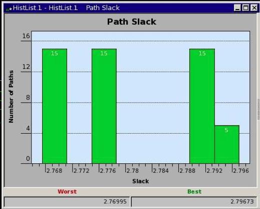
24 Histograms for Slack
Timing Issues in FPGA Synchronous Circuit Design
 ECE 428 Programmable ASIC Design Timing Issues in FPGA Synchronous Circuit Design Haibo Wang ECE Department Southern Illinois University Carbondale, IL 62901 1-1 FPGA Design Flow Schematic capture HDL
Timing analysis can be done right after synthesis. But it can only be accurately done when layout is available
 Timing Analysis Lecture 9 ECE 156A-B 1 General Timing analysis can be done right after synthesis But it can only be accurately done when layout is available Timing analysis at an early stage is not accurate
ENGIN 112 Intro to Electrical and Computer Engineering
 ENGIN 112 Intro to Electrical and Computer Engineering Lecture 28 Timing Analysis Overview Circuits do not respond instantaneously to input changes Predictable delay in transferring inputs to outputs Propagation
INF3430 Clock and Synchronization
 INF3430 Clock and Synchronization P.P.Chu Using VHDL Chapter 16.1-6 INF 3430 - H12 : Chapter 16.1-6 1 Outline 1. Why synchronous? 2. Clock distribution network and skew 3. Multiple-clock system 4. Meta-stability
In this lecture, we will first examine practical digital signals. Then we will discuss the timing constraints in digital systems.
 1 In this lecture, we will first examine practical digital signals. Then we will discuss the timing constraints in digital systems. The important concepts are related to setup and hold times of registers
Geared Oscillator Project Final Design Review. Nick Edwards Richard Wright
 Geared Oscillator Project Final Design Review Nick Edwards Richard Wright This paper outlines the implementation and results of a variable-rate oscillating clock supply. The circuit is designed using a
UNIVERSITY OF BOLTON SCHOOL OF ENGINEERING BENG (HONS) ELECTRICAL & ELECTRONICS ENGINEERING SEMESTER TWO EXAMINATION 2017/2018
 ELECTRICAL & ELECTRONICS ENGINEERING SEMESTER TWO EXAMINATION 2017/2018") UNIVERSITY OF BOLTON [EES04] SCHOOL OF ENGINEERING BENG (HONS) ELECTRICAL & ELECTRONICS ENGINEERING SEMESTER TWO EXAMINATION 2017/2018 INTERMEDIATE DIGITAL ELECTRONICS AND COMMUNICATIONS MODULE NO: EEE5002
UNIVERSITY OF BOLTON [EES04] SCHOOL OF ENGINEERING BENG (HONS) ELECTRICAL & ELECTRONICS ENGINEERING SEMESTER TWO EXAMINATION 2017/2018 INTERMEDIATE DIGITAL ELECTRONICS AND COMMUNICATIONS MODULE NO: EEE5002
Lecture 19: Design for Skew
 Introduction to CMOS VLSI Design Lecture 19: Design for Skew David Harris Harvey Mudd College Spring 2004 Outline Clock Distribution Clock Skew Skew-Tolerant Circuits Traditional Domino Circuits Skew-Tolerant
ECE 551: Digital System Design & Synthesis
 ECE 551: Digital System Design & Synthesis Lecture Set 9 9.1: Constraints and Timing 9.2: Optimization (In separate file) 03/30/03 1 ECE 551 - Digital System Design & Synthesis Lecture 9.1 - Constraints
Reference. Wayne Wolf, FPGA-Based System Design Pearson Education, N Krishna Prakash,, Amrita School of Engineering
 FPGA Fabrics Reference Wayne Wolf, FPGA-Based System Design Pearson Education, 2004 CPLD / FPGA CPLD Interconnection of several PLD blocks with Programmable interconnect on a single chip Logic blocks executes
CS/EE Homework 9 Solutions
 S/EE 260 - Homework 9 Solutions ue 4/6/2000 1. onsider the synchronous ripple carry counter on page 5-8 of the notes. Assume that the flip flops have a setup time requirement of 2 ns and that the gates
Lecture 9: Clocking for High Performance Processors
 Lecture 9: Clocking for High Performance Processors Computer Systems Lab Stanford University horowitz@stanford.edu Copyright 2001 Mark Horowitz EE371 Lecture 9-1 Horowitz Overview Reading Bailey Stojanovic
1 Q' 3. You are given a sequential circuit that has the following circuit to compute the next state:
 UNIVERSITY OF CALIFORNIA Department of Electrical Engineering and Computer Sciences C50 Fall 2001 Prof. Subramanian Homework #3 Due: Friday, September 28, 2001 1. Show how to implement a T flip-flop starting
logic system Outputs The addition of feedback means that the state of the circuit may change with time; it is sequential. logic system Outputs
 Sequential Logic The combinational logic circuits we ve looked at so far, whether they be simple gates or more complex circuits have clearly separated inputs and outputs. A change in the input produces
EDA Challenges for Low Power Design. Anand Iyer, Cadence Design Systems
 EDA Challenges for Low Power Design Anand Iyer, Cadence Design Systems Agenda Introduction ti LP techniques in detail Challenges to low power techniques Guidelines for choosing various techniques Why is
Lecture 02: Digital Logic Review
 CENG 3420 Lecture 02: Digital Logic Review Bei Yu byu@cse.cuhk.edu.hk CENG3420 L02 Digital Logic. 1 Spring 2017 Review: Major Components of a Computer CENG3420 L02 Digital Logic. 2 Spring 2017 Review:
Technology Timeline. Transistors ICs (General) SRAMs & DRAMs Microprocessors SPLDs CPLDs ASICs. FPGAs. The Design Warrior s Guide to.
 SRAMs & DRAMs Microprocessors SPLDs CPLDs ASICs. FPGAs. The Design Warrior s Guide to.") FPGAs 1 CMPE 415 Technology Timeline 1945 1950 1955 1960 1965 1970 1975 1980 1985 1990 1995 2000 Transistors ICs (General) SRAMs & DRAMs Microprocessors SPLDs CPLDs ASICs FPGAs The Design Warrior s Guide
FPGAs 1 CMPE 415 Technology Timeline 1945 1950 1955 1960 1965 1970 1975 1980 1985 1990 1995 2000 Transistors ICs (General) SRAMs & DRAMs Microprocessors SPLDs CPLDs ASICs FPGAs The Design Warrior s Guide
Course Summary. 3213: Digital Systems & Microprocessors: L#14_15
 Course Summary 1. Course overview 2. Intro to PICOBLAZE, C and Number systems and Boolean Algebra 3. Course overview with microprocessor MU0 (I) 4. Course overview with microprocessor MU0 (II) 5. Verilog
EITF35: Introduction to Structured VLSI Design
 EITF35: Introduction to Structured VLSI Design Part 4.2.1: Learn More Liang Liu liang.liu@eit.lth.se 1 Outline Crossing clock domain Reset, synchronous or asynchronous? 2 Why two DFFs? 3 Crossing clock
CHAPTER III THE FPGA IMPLEMENTATION OF PULSE WIDTH MODULATION
 34 CHAPTER III THE FPGA IMPLEMENTATION OF PULSE WIDTH MODULATION 3.1 Introduction A number of PWM schemes are used to obtain variable voltage and frequency supply. The Pulse width of PWM pulsevaries with
Sequential Logic Circuits
 Exercise 2 Sequential Logic Circuits 1 - Introduction Goal of the exercise The goals of this exercise are: - verify the behavior of simple sequential logic circuits; - measure the dynamic parameters of
Audio Sample Rate Conversion in FPGAs
 Audio Sample Rate Conversion in FPGAs An efficient implementation of audio algorithms in programmable logic. by Philipp Jacobsohn Field Applications Engineer Synplicity eutschland GmbH philipp@synplicity.com
Module -18 Flip flops
 1 Module -18 Flip flops 1. Introduction 2. Comparison of latches and flip flops. 3. Clock the trigger signal 4. Flip flops 4.1. Level triggered flip flops SR, D and JK flip flops 4.2. Edge triggered flip
We ve looked at timing issues in combinational logic Let s now examine timing issues we must deal with in sequential circuits
 Basic Timing Issues We ve looked at timing issues in combinational logic Let s now examine timing issues we must deal with in sequential circuits The fundamental timing issues we considered then apply
2014 Paper E2.1: Digital Electronics II
 2014 Paper E2.1: Digital Electronics II Answer ALL questions. There are THREE questions on the paper. Question ONE counts for 40% of the marks, other questions 30% Time allowed: 2 hours (Not to be removed
Sequential Logic Circuits
 LAB EXERCISE - 5 Page 1 of 6 Exercise 5 Sequential Logic Circuits 1 - Introduction Goal of the exercise The goals of this exercise are: - verify the behavior of simple sequential logic circuits; - measure
Low Power Design. Prof. MacDonald
 Low Power Design Prof. MacDonald Power the next challenge! l High performance thermal problems power is now exceeding 100-200 watts l difficult to remove heat from system l slows down circuits - mobilities
Lecture #2 Solving the Interconnect Problems in VLSI
 Lecture #2 Solving the Interconnect Problems in VLSI C.P. Ravikumar IIT Madras - C.P. Ravikumar 1 Interconnect Problems Interconnect delay has become more important than gate delays after 130nm technology
I hope you have completed Part 2 of the Experiment and is ready for Part 3.
 I hope you have completed Part 2 of the Experiment and is ready for Part 3. In part 3, you are going to use the FPGA to interface with the external world through a DAC and a ADC on the add-on card. You
On-silicon Instrumentation
 On-silicon Instrumentation An approach to alleviate the variability problem Peter Y. K. Cheung Department of Electrical and Electronic Engineering 18 th March 2014 U. of York How we started (in 2006)!
Time to Digital Converter Core for Spartan-6 FPGAs
 Time to Digital Converter Core for Spartan-6 FPGAs Sébastien Bourdeauducq November 2011 1 Specifications The Time to Digital Converter (TDC) core is a high precision (sub-nanosecond) time to digital conversion
Metastability. 1
 Metastability talarico@gonzaga.edu 1 Asynchronous Inputs Synchronous circuits can have asynchronous inputs Even a supposedly synchronous circuit like the D flip flop can have asynchronous inputs such as
CMOS Process Variations: A Critical Operation Point Hypothesis
 CMOS Process Variations: A Critical Operation Point Hypothesis Janak H. Patel Department of Electrical and Computer Engineering University of Illinois at Urbana-Champaign jhpatel@uiuc.edu Computer Systems
Logic Synthesis. Logic synthesis transforms RTL code into a gate-level netlist. RTL Verilog converted into Structural Verilog
 Logic Synthesis Logic synthesis transforms RTL code into a gate-level netlist RTL Verilog converted into Structural Verilog Logic Synthesis - The process and steps Translation Check RTL for valid syntax
FINITE IMPULSE RESPONSE (FIR) FILTER
 FILTER") CHAPTER 3 FINITE IMPULSE RESPONSE (FIR) FILTER 3.1 Introduction Digital filtering is executed in two ways, utilizing either FIR (Finite Impulse Response) or IIR (Infinite Impulse Response) Filters (MathWorks
CHAPTER 3 FINITE IMPULSE RESPONSE (FIR) FILTER 3.1 Introduction Digital filtering is executed in two ways, utilizing either FIR (Finite Impulse Response) or IIR (Infinite Impulse Response) Filters (MathWorks
ECE 2300 Digital Logic & Computer Organization
 ECE 2300 Digital Logic & Computer Organization Spring 2018 Timing Analysis Lecture 11: 1 Announcements Lab report guidelines are uploaded on CMS As part of the assignment for Lab 3 report Lab 4(A) prelab
CPE/EE 427, CPE 527 VLSI Design I: Homeworks 3 & 4
 CPE/EE 427, CPE 527 VLSI Design I: Homeworks 3 & 4 1 2 3 4 5 6 7 8 9 10 Sum 30 10 25 10 30 40 10 15 15 15 200 1. (30 points) Misc, Short questions (a) (2 points) Postponing the introduction of signals
Lecture 3, Handouts Page 1. Introduction. EECE 353: Digital Systems Design Lecture 3: Digital Design Flows, Simulation Techniques.
 Introduction EECE 353: Digital Systems Design Lecture 3: Digital Design Flows, Techniques Cristian Grecu grecuc@ece.ubc.ca Course web site: http://courses.ece.ubc.ca/353/ What have you learned so far?
CSE 260 Digital Computers: Organization and Logical Design. Midterm Solutions
 CSE 260 Digital Computers: Organization and Logical Design Midterm Solutions Jon Turner 2/28/2008 1. (10 points). The figure below shows a simulation of the washu-1 processor, with some items blanked out.
Lecture 4&5 CMOS Circuits
 Lecture 4&5 CMOS Circuits Xuan Silvia Zhang Washington University in St. Louis http://classes.engineering.wustl.edu/ese566/ Worst-Case V OL 2 3 Outline Combinational Logic (Delay Analysis) Sequential Circuits
ECE380 Digital Logic
 ECE380 Digital Logic Implementation Technology: Standard Chips and Programmable Logic Devices Dr. D. J. Jackson Lecture 10-1 Standard chips A number of chips, each with a few logic gates, are commonly
Design and implementation of LDPC decoder using time domain-ams processing
 2015; 1(7): 271-276 ISSN Print: 2394-7500 ISSN Online: 2394-5869 Impact Factor: 5.2 IJAR 2015; 1(7): 271-276 www.allresearchjournal.com Received: 31-04-2015 Accepted: 01-06-2015 Shirisha S M Tech VLSI
Digital Systems Design
 Digital Systems Design Clock Networks and Phase Lock Loops on Altera Cyclone V Devices Dr. D. J. Jackson Lecture 9-1 Global Clock Network & Phase-Locked Loops Clock management is important within digital
ECEN 720 High-Speed Links: Circuits and Systems
 1 ECEN 720 High-Speed Links: Circuits and Systems Lab4 Receiver Circuits Objective To learn fundamentals of receiver circuits. Introduction Receivers are used to recover the data stream transmitted by
The Use and Design of Synchronous Mirror Delays. Vince DiPuccio ECG 721 Spring 2017
 The Use and Design of Synchronous Mirror Delays Vince DiPuccio ECG 721 Spring 2017 Presentation Overview Synchronization circuit Topologies covered in class PLL and DLL pros and cons Synchronous mirror
Testing Digital Systems II
 Lecture : Introduction Instructor: M. Tahoori Copyright 206, M. Tahoori TDS II: Lecture Today s Lecture Logistics Course Outline Review from TDS I Copyright 206, M. Tahoori TDS II: Lecture 2 Lecture Logistics
PROCESS-VOLTAGE-TEMPERATURE (PVT) VARIATIONS AND STATIC TIMING ANALYSIS
 VARIATIONS AND STATIC TIMING ANALYSIS") PROCESS-VOLTAGE-TEMPERATURE (PVT) VARIATIONS AND STATIC TIMING ANALYSIS The major design challenges of ASIC design consist of microscopic issues and macroscopic issues [1]. The microscopic issues are ultra-high
PROCESS-VOLTAGE-TEMPERATURE (PVT) VARIATIONS AND STATIC TIMING ANALYSIS The major design challenges of ASIC design consist of microscopic issues and macroscopic issues [1]. The microscopic issues are ultra-high
Sensing Voltage Transients Using Built-in Voltage Sensor
 Sensing Voltage Transients Using Built-in Voltage Sensor ABSTRACT Voltage transient is a kind of voltage fluctuation caused by circuit inductance. If strong enough, voltage transients can cause system
12 BIT ACCUMULATOR FOR DDS
 12 BIT ACCUMULATOR FOR DDS ECE547 Final Report Aravind Reghu Spring, 2006 1 CONTENTS 1 Introduction 6 1.1 Project Overview 6 1.1.1 How it Works 6 1.2 Objective 8 2 Circuit Design 9 2.1 Design Objective
An Overview of the NASA Goddard Methodology for FPGA Radiation Testing and Soft Error Rate (SER) Prediction
 Prediction") An Overview of the NASA Goddard Methodology for FPGA Radiation Testing and Soft Error Rate (SER) Prediction Melanie Berg, MEI Technologies in support of NASA/GSFC To be presented by Melanie Berg at the
An Overview of the NASA Goddard Methodology for FPGA Radiation Testing and Soft Error Rate (SER) Prediction Melanie Berg, MEI Technologies in support of NASA/GSFC To be presented by Melanie Berg at the
R Using the Virtex Delay-Locked Loop
 Application Note: Virtex Series XAPP132 (v2.4) December 20, 2001 Summary The Virtex FPGA series offers up to eight fully digital dedicated on-chip Delay-Locked Loop (DLL) circuits providing zero propagation
Managing Cross-talk Noise
 Managing Cross-talk Noise Rajendran Panda Motorola Inc., Austin, TX Advanced Tools Organization Central in-house CAD tool development and support organization catering to the needs of all design teams
CHAPTER 16 SEQUENTIAL CIRCUIT DESIGN. Click the mouse to move to the next page. Use the ESC key to exit this chapter.
 CHPTER 6 SEQUENTIL CIRCUIT DESIGN Click the mouse to move to the next page. Use the ESC key to exit this chapter. Contents 6. Summary of Design Procedure for Sequential Circuits 6.2 Design ExampleCode
VLSI Design 11. Sequential Elements
 VLSI esign Last module: Wire resistance and capacitance RC delay Wire gineering This module Floorplanning (basic physical design determines wires) Sequtial circuit design Clock skew Floorplan How do you
! Review: Sequential MOS Logic. " SR Latch. " D-Latch. ! Timing Hazards. ! Dynamic Logic. " Domino Logic. ! Charge Sharing Setup.
 ESE 570: Digital Integrated Circuits and VLSI Fundamentals Lec 9: March 29, 206 Timing Hazards and Dynamic Logic Lecture Outline! Review: Sequential MOS Logic " SR " D-! Timing Hazards! Dynamic Logic "
EECS 270: Lab 7. Real-World Interfacing with an Ultrasonic Sensor and a Servo
 EECS 270: Lab 7 Real-World Interfacing with an Ultrasonic Sensor and a Servo 1. Overview The purpose of this lab is to learn how to design, develop, and implement a sequential digital circuit whose purpose
EECS 427 Lecture 22: Low and Multiple-Vdd Design
 EECS 427 Lecture 22: Low and Multiple-Vdd Design Reading: 11.7.1 EECS 427 W07 Lecture 22 1 Last Time Low power ALUs Glitch power Clock gating Bus recoding The low power design space Dynamic vs static EECS
Basic Logic Circuits
 Basic Logic Circuits Required knowledge Measurement of static characteristics of nonlinear circuits. Measurement of current consumption. Measurement of dynamic properties of electrical circuits. Definitions
The challenges of low power design Karen Yorav
 The challenges of low power design Karen Yorav The challenges of low power design What this tutorial is NOT about: Electrical engineering CMOS technology but also not Hand waving nonsense about trends
IES Digital Mock Test
 . The circuit given below work as IES Digital Mock Test - 4 Logic A B C x y z (a) Binary to Gray code converter (c) Binary to ECESS- converter (b) Gray code to Binary converter (d) ECESS- To Gray code
Digital Design and System Implementation. Overview of Physical Implementations
 Digital Design and System Implementation Overview of Physical Implementations CMOS devices CMOS transistor circuit functional behavior Basic logic gates Transmission gates Tri-state buffers Flip-flops
Programmable Interconnect. CPE/EE 428, CPE 528: Session #13. Actel Programmable Interconnect. Actel Programmable Interconnect
 Programmable Interconnect CPE/EE 428, CPE 528: Session #13 Department of Electrical and Computer Engineering University of Alabama in Huntsville In addition to programmable cells, programmable ASICs must
ECE520 VLSI Design. Lecture 11: Combinational Static Logic. Prof. Payman Zarkesh-Ha
 EE520 VLSI esign Lecture 11: ombinational Static Logic Prof. Payman Zarkesh-Ha Office: EE ldg. 230 Office hours: Wednesday 2:00-3:00PM or by appointment E-mail: pzarkesh@unm.edu Slide: 1 eview of Last
FPGA Based System Design
 FPGA Based System Design Reference Wayne Wolf, FPGA-Based System Design Pearson Education, 2004 Why VLSI? Integration improves the design: higher speed; lower power; physically smaller. Integration reduces
Accurate Timing and Power Characterization of Static Single-Track Full-Buffers
 Accurate Timing and Power Characterization of Static Single-Track Full-Buffers By Rahul Rithe Department of Electronics & Electrical Communication Engineering Indian Institute of Technology Kharagpur,
Project Board Game Counter: Digital
 Project 1.3.3 Board Game Counter: Digital Introduction Just a few short weeks ago, most of you knew little or nothing about digital electronics. Now you are about to build and simulate a complete design.
Introduction to CMOS VLSI Design (E158) Lecture 5: Logic
 Lecture 5: Logic") Harris Introduction to CMOS VLSI Design (E158) Lecture 5: Logic David Harris Harvey Mudd College David_Harris@hmc.edu Based on EE271 developed by Mark Horowitz, Stanford University MAH E158 Lecture 5 1
Harris Introduction to CMOS VLSI Design (E158) Lecture 5: Logic David Harris Harvey Mudd College David_Harris@hmc.edu Based on EE271 developed by Mark Horowitz, Stanford University MAH E158 Lecture 5 1
ELEC Digital Logic Circuits Fall 2015 Delay and Power
 ELEC - Digital Logic Circuits Fall 5 Delay and Power Vishwani D. Agrawal James J. Danaher Professor Department of Electrical and Computer Engineering Auburn University, Auburn, AL 36849 http://www.eng.auburn.edu/~vagrawal
Microcircuit Electrical Issues
 Microcircuit Electrical Issues Distortion The frequency at which transmitted power has dropped to 50 percent of the injected power is called the "3 db" point and is used to define the bandwidth of the
SRV ENGINEERING COLLEGE SEMBODAI RUKMANI VARATHARAJAN ENGINEERING COLLEGE SEMBODAI
 SEMBODAI RUKMANI VARATHARAJAN ENGINEERING COLLEGE SEMBODAI 6489 (Approved By AICTE,Newdelhi Affiliated To ANNA UNIVERSITY::Chennai) CS 62 DIGITAL ELECTRONICS LAB (REGULATION-23) LAB MANUAL DEPARTMENT OF
PE713 FPGA Based System Design
 PE713 FPGA Based System Design Why VLSI? Dept. of EEE, Amrita School of Engineering Why ICs? Dept. of EEE, Amrita School of Engineering IC Classification ANALOG (OR LINEAR) ICs produce, amplify, or respond
MICROWIND2 DSCH2 8. Converters /11/00
 8-9 05/11/00 Fig. 8-7. Effect of sampling The effect of sample and hold is illustrated in figure 8-7. When sampling, the transmission gate is turned on so that the sampled data DataOut reaches the value
IJITKMI Volume 6 Number 2 July-December 2013 pp FPGA-based implementation of UART
 FPGA-based implementation of UART Kamal Kumar Sharma 1 Parul Sharma 2 1 Professor; 2 Assistant Professor Dept. of Electronics and Comm Engineering, E-max School of Engineering and Applied Research, Ambala
Multi-Channel FIR Filters
 Chapter 7 Multi-Channel FIR Filters This chapter illustrates the use of the advanced Virtex -4 DSP features when implementing a widely used DSP function known as multi-channel FIR filtering. Multi-channel
! Sequential Logic. ! Timing Hazards. ! Dynamic Logic. ! Add state elements (registers, latches) ! Compute. " From state elements
 ! Compute. From state elements") ESE 570: Digital Integrated Circuits and VLSI Fundamentals Lec 19: April 2, 2019 Sequential Logic, Timing Hazards and Dynamic Logic Lecture Outline! Sequential Logic! Timing Hazards! Dynamic Logic 4 Sequential
ESE 570: Digital Integrated Circuits and VLSI Fundamentals Lec 19: April 2, 2019 Sequential Logic, Timing Hazards and Dynamic Logic Lecture Outline! Sequential Logic! Timing Hazards! Dynamic Logic 4 Sequential
1/19/2012. Timing in Asynchronous Circuits
 Timing in Asynchronous Circuits 1 What do we mean by clock? The system clock for an integrated circuit is a voltage signal that pulses at a regular frequency. 1 0 Time The clock tells each stage of a circuit
PRESENTATION OF THE PROJECTX-FINAL LEVEL 1.
 Implementation of digital it frequency dividersid PRESENTATION OF THE PROJECTX-FINAL LEVEL 1. Why frequency divider? Motivation widely used in daily life Time counting (electronic clocks, traffic lights,
Mohit Arora. The Art of Hardware Architecture. Design Methods and Techniques. for Digital Circuits. Springer
 Mohit Arora The Art of Hardware Architecture Design Methods and Techniques for Digital Circuits Springer Contents 1 The World of Metastability 1 1.1 Introduction 1 1.2 Theory of Metastability 1 1.3 Metastability
EE584 Introduction to VLSI Design Final Project Document Group 9 Ring Oscillator with Frequency selector
 EE584 Introduction to VLSI Design Final Project Document Group 9 Ring Oscillator with Frequency selector Group Members Uttam Kumar Boda Rajesh Tenukuntla Mohammad M Iftakhar Srikanth Yanamanagandla 1 Table
Lecture 11: Clocking
 High Speed CMOS VLSI Design Lecture 11: Clocking (c) 1997 David Harris 1.0 Introduction We have seen that generating and distributing clocks with little skew is essential to high speed circuit design.
EC4205 Microprocessor and Microcontroller
 EC4205 Microprocessor and Microcontroller Webcast link: https://sites.google.com/a/bitmesra.ac.in/aminulislam/home All announcement made through webpage: check back often Students are welcome outside the
EE382M VLSI- II. EDP- TC: Early Design Planning for Timing Closure. Spring Mark McDermoF. EE382M- 8 Class Notes
 EE382M VLSI- II EDP- TC: Early Design Planning for Timing Closure Spring 2017 Mark McDermoF EE382M- 8 Class Notes Agenda: Early Design Planning for Timing Closure Basics of Timing EDP- TC What is It? EDP-
CSE241 VLSI Digital Circuits Winter Lecture 06: Timing
 CSE241 VLSI Digital Circuits Winter 2003 Lecture 06: Timing CSE241 L3 ASICs.1 Kahng & Cichy, UCSD 2003 This Class + Logistics Timing Flip-flop timing Clock distribution Clock tree synthesis Reading: White
PROGRAMMABLE ASICs. Antifuse SRAM EPROM
 PROGRAMMABLE ASICs FPGAs hold array of basic logic cells Basic cells configured using Programming Technologies Programming Technology determines basic cell and interconnect scheme Programming Technologies
EECS150 - Digital Design Lecture 19 CMOS Implementation Technologies. Recap and Outline
 EECS150 - Digital Design Lecture 19 CMOS Implementation Technologies Oct. 31, 2013 Prof. Ronald Fearing Electrical Engineering and Computer Sciences University of California, Berkeley (slides courtesy
ECEN 720 High-Speed Links Circuits and Systems
 1 ECEN 720 High-Speed Links Circuits and Systems Lab4 Receiver Circuits Objective To learn fundamentals of receiver circuits. Introduction Receivers are used to recover the data stream transmitted by transmitters.
ACEX 1K. Features... Programmable Logic Device Family. Tools
 ACEX 1K Programmable Logic Device Family May 2003, ver. 3.4 Data Sheet Features... Programmable logic devices (PLDs), providing low cost system-on-a-programmable-chip (SOPC) integration in a single device
LOGIC DIAGRAM: HALF ADDER TRUTH TABLE: A B CARRY SUM. 2012/ODD/III/ECE/DE/LM Page No. 1
 LOGIC DIAGRAM: HALF ADDER TRUTH TABLE: A B CARRY SUM K-Map for SUM: K-Map for CARRY: SUM = A B + AB CARRY = AB 22/ODD/III/ECE/DE/LM Page No. EXPT NO: DATE : DESIGN OF ADDER AND SUBTRACTOR AIM: To design
ICCAD 2014 Contest Incremental Timing-driven Placement: Timing Modeling and File Formats v1.1 April 14 th, 2014
 ICCAD 2014 Contest Incremental Timing-driven Placement: Timing Modeling and File Formats v1.1 April 14 th, 2014 http://cad contest.ee.ncu.edu.tw/cad-contest-at-iccad2014/problem b/ 1 Introduction This
Maximum data rate: 50 MBaud Data rate range: ±15% Lock-in time: 1 bit
 MONOLITHIC MANCHESTER ENCODER/DECODER (SERIES 3D7503) FEATURES 3D7503 data 3 delay devices, inc. PACKAGES All-silicon, low-power CMOS technology CIN 1 14 Encoder and decoder function independently Encoder
ACEX 1K. Features... Programmable Logic Family. Tools. Table 1. ACEX TM 1K Device Features
 ACEX 1K Programmable Logic Family March 2000, ver. 1 Data Sheet Features... Programmable logic devices (PLDs), providing low cost system-on-a-programmable-chip integration in a single device Enhanced embedded
Lecture 1. Tinoosh Mohsenin
 Lecture 1 Tinoosh Mohsenin Today Administrative items Syllabus and course overview Digital systems and optimization overview 2 Course Communication Email Urgent announcements Web page http://www.csee.umbc.edu/~tinoosh/cmpe650/
UNIT-II LOW POWER VLSI DESIGN APPROACHES
 UNIT-II LOW POWER VLSI DESIGN APPROACHES Low power Design through Voltage Scaling: The switching power dissipation in CMOS digital integrated circuits is a strong function of the power supply voltage.
FPGA IMPLEMENTATION OF POWER EFFICIENT ALL DIGITAL PHASE LOCKED LOOP
 INTERNATIONAL JOURNAL OF ELECTRONICS AND COMMUNICATION ENGINEERING & TECHNOLOGY (IJECET) Proceedings of the International Conference on Emerging Trends in Engineering and Management (ICETEM14) ISSN 0976
CS 61C: Great Ideas in Computer Architecture Finite State Machines, Functional Units
 CS 61C: Great Ideas in Computer Architecture Finite State Machines, Functional Units Instructors: Vladimir Stojanovic and Nicholas Weaver http://inst.eecs.berkeley.edu/~cs61c/sp16 1 Machine Interpretation
EE 434 ASIC and Digital Systems. Prof. Dae Hyun Kim School of Electrical Engineering and Computer Science Washington State University.
 EE 434 ASIC and Digital Systems Prof. Dae Hyun Kim School of Electrical Engineering and Computer Science Washington State University Preliminaries VLSI Design System Specification Functional Design RTL
Controller Implementation--Part I. Cascading Edge-triggered Flip-Flops
 Controller Implementation--Part I Alternative controller FSM implementation approaches based on: Classical Moore and Mealy machines Time state: Divide and Counter Jump counters Microprogramming (ROM) based
VLSI IMPLEMENTATION OF MODIFIED DISTRIBUTED ARITHMETIC BASED LOW POWER AND HIGH PERFORMANCE DIGITAL FIR FILTER Dr. S.Satheeskumaran 1 K.
 VLSI IMPLEMENTATION OF MODIFIED DISTRIBUTED ARITHMETIC BASED LOW POWER AND HIGH PERFORMANCE DIGITAL FIR FILTER Dr. S.Satheeskumaran 1 K. Sasikala 2 1 Professor, Department of Electronics and Communication
PV SYSTEM BASED FPGA: ANALYSIS OF POWER CONSUMPTION IN XILINX XPOWER TOOL
 1 PV SYSTEM BASED FPGA: ANALYSIS OF POWER CONSUMPTION IN XILINX XPOWER TOOL Pradeep Patel Instrumentation and Control Department Prof. Deepali Shah Instrumentation and Control Department L. D. College
A Digital Clock Multiplier for Globally Asynchronous Locally Synchronous Designs
 A Digital Clock Multiplier for Globally Asynchronous Locally Synchronous Designs Thomas Olsson, Peter Nilsson, and Mats Torkelson. Dept of Applied Electronics, Lund University. P.O. Box 118, SE-22100,