Recent ETHZ-YEBES Developments in Low-Noise phemts for Cryogenic Amplifiers
|
|
|
- Jared Collins
- 5 years ago
- Views:
Transcription
 ETH-Zürich, Gloriastrasse 35, Zürich 8092, Switzerland http://www.mwe.ee.ethz.")
1 Receivers & Array Workshop 2010 September 20th, 2010 Recent ETHZ-YEBES Developments in Low-Noise phemts for Cryogenic Amplifiers Andreas R. Alt, Colombo R. Bolognesi Millimeter-Wave Electronics Group (MWE) ETH-Zürich, Gloriastrasse 35, Zürich 8092, Switzerland 1
2 Outline Group and Lab Introduction ETH HEMT Process & Fabrication Device Characteristics YEBES Amplifier Results Conclusion 2
3 Introducing MWE Group Established in 2006 Members (9 Researchers + 1 Prof) 7 Ph.D. Candidates 2 Postdocs 1 Measurement Engineer + 1 Process Engineer Research Areas HEMTs (InP, Group III-N) InP/GaAsSb DHBTs MOCVD (InP, GaInP, GaAsSb) Circuit Design + Characterization 3

4 Introducing ETH / FIRST Cleanroom FIRST Frontiers in Research Space and Time In Operation since m 2 of class State of the Art Equipment Managed by 11 Professors Run by 9 perm. Employees 4

5 Introducing ETH / FIRST Cleanroom Equipment 3 MBEs / MOVPE 2 X-Ray / PL Mapper 2 Zeiss SEMs / AFM 2 Raith 30kV EBLs PECVD / RIEs / ICP / LPCVD / ALD 3 EB-Evaporation / 1 Sputter System Rapid Thermal Annealer CV-Profiler / Hall Effect System Ellipsometer / Alphastep MA6 / MJB3 / DUV Aligners 3 Optical Microscopes Wet Bench Area / Litho Area 5
6 Introducing ETH / MWE Measurement Lab Measurement Tools & Capabilities Vector Network Analyzers ( GHz GHz) Power Analysis ( GHz) Spectrum Measurements up to 90 GHz Antenna Measurements Noise Figure Measurements up to 75 GHz Noise Parameters up to 20 GHz Up to 50 GHz by End of 2010 Multiharmonic Load-Source Pull by End of
7 Introducing ETH / MWE Cryo Lab On-Wafer Calibration System Open-Cycle Cryostat Vacuum Level: <10-6 Torr Temperature Range: 5 K to 400 K (±0.1K) PID Temperature Controller Temperature Sensors: Si Diode (Chuck) and Pt Thermometer (Probe Arm) Feedthrough: RF Cables (K- and 2.4mm-connector) DC Wires/Cables (10 pin) Probes Cryogenic RF Probes (K- and 2.4mm connector) Multi-Contact-Wedge Probe (9 pin) 7
 2 DC Wires/Cables (16 pin) Probes Any Probe Type Fitting on the Copper Plate (Ø17cm x 10")
8 Introducing ETH / MWE Cryo Lab Cryo Dewar System Temperature Range: 10 K to 400 K Feedthrough: 4 RF Cables (SMA-connectors) 2 DC Wires/Cables (16 pin) Probes Any Probe Type Fitting on the Copper Plate (Ø17cm x 10 cm) 8
9 Outline Group and Lab Introduction ETH HEMT Process & Fabrication Device Characteristics YEBES Amplifier Results Conclusion 9
10 ETH HEMT History 1991 Development of 0.25µm ETH AlInAs/GaInAs/InP HEMT Transistor-Process by C. Bergamaschi under Prof. Bächtold 1998 First ESA-Project Involving ETH-HEMTs and YEBES for Design & Fabrication of X-Band Amplifier Process Transfer from In-House Cleanroom to FIRST Currently: ESA Ka-Band Amplifier Project with ETH Devices and YEBES for Amplifier Design & Fabrication (S. Halté) 10
11 ETH InP HEMT Work Today Evolve Conventional AlInAs/GaInAs/InP HEMT Technology InAs Channel Insets Without Antimonide Related Problems Aluminum Free GaInP/GaInAs phemt Concept for Improved: High-Frequency Power Performance Reliability LF-Noise Cryo Performance Breakdown Behavior Improved Etch-Selectivity of GaInAs/GaInP (Recess) 11


12 Aluminum free HEMT Concept Goal: Eliminate AlInAs from HEMT-Epi 12
13 Al-Free InP phemts Motivation: AlInAs Can Be Chemically Unstable Traps Present (Residual Oxygen) Device Instabilities/Non-Idealities (e.g. Kink, Light Sensitivity, etc.) Reliability Limiter InP Buffer Layer Advantages Al-Free 10x Higher Thermal Conductivity wrt Alloys Old Idea: Explored by K. Heime in 1990 s f T = 150 GHz Claimed to Offer Lower Noise than AlInAs/GaInAs HEMTs Did Not Gain Acceptance 13
14 Al-Free InP phemts (ETH-Grown) f MAX > 600 GHz (100 nm) Peak f T Bias: f T = f MAX = 250 GHz Peak f MAX Bias: V DS = 1.5 V f T = 200 GHz / f MAX = 602 GHz Non-Optimized Layers on InP:Fe µ = 8,300 cm 2 /Vs N s < 1 x /cm µm x (2 x 75 µm) L SD = 2 µm The GaInP/GaInAs Al-Free phemt on InP:Fe is Very Promising! 14
15 Typical Device Fabrication Process Ohmic Contacts substrate Ge/Au Annealed Contacts: <0.1 Ωmm Device Isolation Phosphoric Acid Based Solutions Gate Recess Organic Acids T-Gates nm Ebeam T-Gates + SiN x Passivation Metallization Overlay Metallization Electroplating Airbridges +Thick Pad-Metal Followed by Thinning to 100µm + Dicing 15


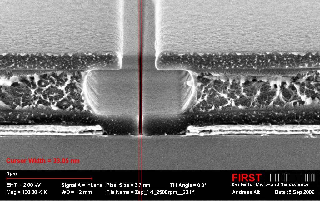
16 InP phemt with L G = 100 nm Electron Beam Lithography 30 nm T-Gate in ZEP-Based Tri-Layer Raith150-Two: Installed End
17 Nanometric Gates 17

18 6 Finger Air-Bridge Device InP phemt (0.1µm x 100µm) 18

19 6 Finger Air-Bridge Device 19
20 Outline Group and Lab Introduction ETH HEMT Process & Fabrication Device Characteristics YEBES Amplifier Results Conclusion 20
21 DC Device RT 21
22 DC Device RT 22
23 DC Device RT 23
24 RF Device RT Bias Sweep Without Removing Pad-Parasitics! 0.1µm x 150µm 24
25 RF Device RT Bias Sweep Without Removing Pad-Parasitics! 0.1µm x 150µm 25
26 DC Device 15K 26
27 DC Device 15K 27

28 DC Device 15K Impact Ionization (V DS 1V 28
29 Effect of Temperature on DC 29
30 Effect of Temperature on DC 30

31 RF Device 15K Bias Sweep Without Removing Pad-Parasitics! 0.1µm x 150µm 31
32 RF Device 15K Bias Sweep Without Removing Pad-Parasitics! 0.1µm x 150µm 32
33 RF Device 15K RF Data Without Removing Pad-Parasitics! F T of V V DS, 0.2V V GS 31mA I DS, 0.12nA I GS 33
34 RF Device 15K RF Data Without Removing Pad-Parasitics! Typical Low-Noise Bias 0.3V V DS, 0.05V V GS 4.3mA I DS, 0.014nA I GS F T = 156 GHz 34
35 Processing Impact on Device Characteristics A Single Process Step Can Have a Dramatic Impact on Gate Leakage! (Everything Else Kept the Same) 35
36 Processing Impact on Device Characteristics A Single Process Step Can Have a Dramatic Impact on Gate Leakage! (Everything Else Kept the Same) 36

37 Processing Impact on Device Characteristics In this Experiment the Processing Change Solely Influenced the Gate Leakage which is a Key Factor for the Noise Performance! 37
38 Outline Group and Lab Introduction ETH HEMT Process & Fabrication Device Characteristics YEBES Amplifier Results Conclusion 38
39 Result Considerations CRYO3 is Considered the Best Transistor Ever Measured Devices Presented Here are not Yet Optimal : Source-Drain Distance is 2µm; Better Performance Expected for 1µm Noise Characterization Over GHz by YEBES YEBES Used ETH Devices in the First Stage of their YK Amplifier, Comparing Against HRL and NGST Devices 39

40 YEBES Amplifier 300K CRYO3 HRL 40

41 YEBES Amplifier 15K HRL CRYO3 41
42 ETHZ-YEBES Measurement Results Noise Results Obtained with ETH Devices Almost Reach CRYO3 The Average in-band Noise is Slightly Higher than CRYO3 The Minimum Noise is in Some Cases Slightly Better than CRYO3 Gain is Significantly Higher for ETH Devices Very Low Gate Leakage at Cryogenic Temperatures 42
43 Outline Group and Lab Introduction ETH HEMT Process & Fabrication Device Characteristics YEBES Amplifier Results Conclusion 43
44 Conclusion ITAR Complicates HEMT Procurement Outside US ETHZ Technology as EU Source of High-Performance Devices Radio-Astronomy & Deep Space Network Telecommunications Research Applications MWE / ETH Interested in Collaborative Projects Secure/Expand EU Source for Strategic Technology Extend Technological Limits 44
GaN MMIC PAs for MMW Applicaitons
 GaN MMIC PAs for MMW Applicaitons Miroslav Micovic HRL Laboratories LLC, 311 Malibu Canyon Road, Malibu, CA 9265, U. S. A. mmicovic@hrl.com Motivation for High Frequency Power sources 6 GHz 11 GHz Frequency
Welcome to. A facility within the Nanometer Structure Consortium (nmc) at Lund University. nanolab. lund
 at Lund University. nanolab. lund") lund nanolab Welcome to A facility within the Nanometer Structure Consortium (nmc) at Lund University »It s a dream come true. This is the lab I always dreamt of. I didn t know it would ever exist.«ivan
lund nanolab Welcome to A facility within the Nanometer Structure Consortium (nmc) at Lund University »It s a dream come true. This is the lab I always dreamt of. I didn t know it would ever exist.«ivan
Gigahertz Ambipolar Frequency Multiplier Based on Cvd Graphene
 Gigahertz Ambipolar Frequency Multiplier Based on Cvd Graphene The MIT Faculty has made this article openly available. Please share how this access benefits you. Your story matters. Citation As Published
SUPPLEMENTARY INFORMATION
 SUPPLEMENTARY INFORMATION doi:10.1038/nature11293 1. Formation of (111)B polar surface on Si(111) for selective-area growth of InGaAs nanowires on Si. Conventional III-V nanowires (NWs) tend to grow in
GaN power electronics
 GaN power electronics The MIT Faculty has made this article openly available. Please share how this access benefits you. Your story matters. Citation As Published Publisher Lu, Bin, Daniel Piedra, and
Ion Beam Lithography next generation nanofabrication
 Ion Beam Lithography next generation nanofabrication EFUG Bordeaux 2011 ion beams develop Lloyd Peto IBL sales manager Copyright 2011 by Raith GmbH ionline new capabilities You can now Apply an ion beam
Micro-PackS, Technology Platform. Security Characterization Lab Opening
 September, 30 th 2008 Micro-PackS, Technology Platform Security Characterization Lab Opening Members : Micro-PackS in SCS cluster From Silicium to innovative & commucating device R&D structure, gathering
Gallium nitride (GaN)
") 80 Technology focus: GaN power electronics Vertical, CMOS and dual-gate approaches to gallium nitride power electronics US research company HRL Laboratories has published a number of papers concerning
80 Technology focus: GaN power electronics Vertical, CMOS and dual-gate approaches to gallium nitride power electronics US research company HRL Laboratories has published a number of papers concerning
Superconducting Nanowire Single Photon Detector (SNSPD) integrated with optical circuits
 integrated with optical circuits") Superconducting Nanowire Single Photon Detector (SNSPD) integrated with optical circuits Marcello Graziosi, ESR 3 within PICQUE (Marie Curie ITN project) and PhD student marcello.graziosi@ifn.cnr.it Istituto
Superconducting Nanowire Single Photon Detector (SNSPD) integrated with optical circuits Marcello Graziosi, ESR 3 within PICQUE (Marie Curie ITN project) and PhD student marcello.graziosi@ifn.cnr.it Istituto
Wu Lu Department of Electrical and Computer Engineering and Microelectronics Laboratory, University of Illinois, Urbana, Illinois 61801
 Comparative study of self-aligned and nonself-aligned SiGe p-metal oxide semiconductor modulation-doped field effect transistors with nanometer gate lengths Wu Lu Department of Electrical and Computer
Sub-30 nm InAs Quantum-Well MOSFETs with Self-Aligned Metal Contacts and Sub-1 nm EOT HfO 2 Insulator
 Sub-30 nm InAs Quantum-Well MOSFETs with Self-Aligned Metal Contacts and Sub-1 nm EOT HfO 2 Insulator Jianqiang Lin, Dimitri A. Antoniadis, and Jesús A. del Alamo Microsystems Technology Laboratories,
Ultra High-Speed InGaAs Nano-HEMTs
 Ultra High-Speed InGaAs Nano-HEMTs 2003. 10. 14 Kwang-Seok Seo School of Electrical Eng. and Computer Sci. Seoul National Univ., Korea Contents Introduction to InGaAsNano-HEMTs Nano Patterning Process
Pattern Transfer CD-AFM. Resist Features on Poly. Poly Features on Oxide. Quate Group, Stanford University
 Resist Features on Poly Pattern Transfer Poly Features on Oxide CD-AFM The Critical Dimension AFM Boot -Shaped Tip Tip shape is optimized to sense topography on vertical surfaces Two-dimensional feedback
Mobile Electrostatic Carrier (MEC) evaluation for a GaAs wafer backside manufacturing process
 evaluation for a GaAs wafer backside manufacturing process") Mobile Electrostatic Carrier (MEC) evaluation for a GaAs wafer backside manufacturing process H.Stieglauer 1, J.Nösser 1, A.Miller 1, M.Lanz 1, D.Öttlin 1, G.Jonsson 1, D.Behammer 1, C.Landesberger 2,
Mobile Electrostatic Carrier (MEC) evaluation for a GaAs wafer backside manufacturing process H.Stieglauer 1, J.Nösser 1, A.Miller 1, M.Lanz 1, D.Öttlin 1, G.Jonsson 1, D.Behammer 1, C.Landesberger 2,
3-7 Nano-Gate Transistor World s Fastest InP-HEMT
 3-7 Nano-Gate Transistor World s Fastest InP-HEMT SHINOHARA Keisuke and MATSUI Toshiaki InP-based InGaAs/InAlAs high electron mobility transistors (HEMTs) which can operate in the sub-millimeter-wave frequency
III-Nitride microwave switches Grigory Simin
 Microwave Microelectronics Laboratory Department of Electrical Engineering, USC Research Focus: - Wide Bandgap Microwave Power Devices and Integrated Circuits - Physics, Simulation, Design and Characterization
A 77 GHz mhemt MMIC Chip Set for Automotive Radar Systems
 A 77 GHz mhemt MMIC Chip Set for Automotive Radar Systems Dong Min Kang, Ju Yeon Hong, Jae Yeob Shim, Jin-Hee Lee, Hyung-Sup Yoon, and Kyung Ho Lee A monolithic microwave integrated circuit (MMIC) chip
Chapter 1. Introduction
 Chapter 1 Introduction 1.1 Introduction of Device Technology Digital wireless communication system has become more and more popular in recent years due to its capability for both voice and data communication.
Nanostencil Lithography and Nanoelectronic Applications
 Microsystems Laboratory Nanostencil Lithography and Nanoelectronic Applications Oscar Vazquez, Marc van den Boogaart, Dr. Lianne Doeswijk, Prof. Juergen Brugger, LMIS1 Dr. Chan Woo Park, Visiting Professor
Room-Temperature-Processed Flexible Amorphous InGaZnO Thin Film Transistor
 Supporting Information Room-Temperature-Processed Flexible Amorphous InGaZnO Thin Film Transistor Xiang Xiao 1, Letao Zhang 1, Yang Shao 1, Xiaoliang Zhou 2, Hongyu He 1, and Shengdong Zhang 1,2 * 1 School
Customized probe card for on-wafer testing of AlGaN/GaN power transistors
 Customized probe card for on-wafer testing of AlGaN/GaN power transistors R. Venegas 1, K. Armendariz 2, N. Ronchi 1 1 imec, 2 Celadon Systems Inc. Outline Introduction GaN for power switching applications
PERSPECTIVES FOR DISRUPTIVE 200MM/8-INCH GAN POWER DEVICE AND GAN-IC TECHNOLOGY DR. DENIS MARCON SR. BUSINESS DEVELOPMENT MANAGER
 PERSPECTIVES FOR DISRUPTIVE 200MM/8-INCH GAN POWER DEVICE AND GAN-IC TECHNOLOGY DR. DENIS MARCON SR. BUSINESS DEVELOPMENT MANAGER What I will show you today 200mm/8-inch GaN-on-Si e-mode/normally-off technology
mhemt based MMICs, Modules, and Systems for mmwave Applications Axel Hülsmann Axel Tessmann Jutta Kühn Oliver Ambacher
 mhemt based MMICs, Modules, and Systems for mmwave Applications Christaweg 54 79114 Freiburg, Germany +49 761 5951 4692 info@ondosense.com www.ondosense.com Axel Hülsmann Axel Tessmann Jutta Kühn Oliver
International Workshop on Nitride Semiconductors (IWN 2016)
") International Workshop on Nitride Semiconductors (IWN 2016) Sheng Jiang The University of Sheffield Introduction The 2016 International Workshop on Nitride Semiconductors (IWN 2016) conference is held
International Workshop on Nitride Semiconductors (IWN 2016) Sheng Jiang The University of Sheffield Introduction The 2016 International Workshop on Nitride Semiconductors (IWN 2016) conference is held
Customized probe card for on wafer testing of AlGaN/GaN power transistors
 Customized probe card for on wafer testing of AlGaN/GaN power transistors R. Venegas 1, K. Armendariz 2, N. Ronchi 1 1 imec, 2 Celadon Systems Inc. Presented by Bryan Root 2 Outline Introduction GaN for
Si and InP Integration in the HELIOS project
 Si and InP Integration in the HELIOS project J.M. Fedeli CEA-LETI, Grenoble ( France) ECOC 2009 1 Basic information about HELIOS HELIOS photonics ELectronics functional Integration on CMOS www.helios-project.eu
Characterizing Fabrication Process Induced Effects in Deep Submicron PHEMT's Using Spectrally Resolved Light Emission Imaging
 Characterizing Fabrication Process Induced Effects in Deep Submicron PHEMT's Using Spectrally Resolved Light Emission Imaging Zhuyi Wang, Weidong Cai, Mengwei Zhang and G.P. Li Department of Electrical
InGaAs MOSFETs for CMOS:
 InGaAs MOSFETs for CMOS: Recent Advances in Process Technology J. A. del Alamo, D. Antoniadis, A. Guo, D.-H. Kim 1, T.-W. Kim 2, J. Lin, W. Lu, A. Vardi and X. Zhao Microsystems Technology Laboratories,
MMA RECEIVERS: HFET AMPLIFIERS
 MMA Project Book, Chapter 5 Section 4 MMA RECEIVERS: HFET AMPLIFIERS Marian Pospieszalski Ed Wollack John Webber Last revised 1999-04-09 Revision History: 1998-09-28: Added chapter number to section numbers.
Supplementary Information
 Supplementary Information Wireless thin film transistor based on micro magnetic induction coupling antenna Byoung Ok Jun 1, Gwang Jun Lee 1, Jong Gu Kang 1,2, Seung Uk Kim 1, Ji Woong Choi 1, Seung Nam
State-of-the-art device fabrication techniques
 State-of-the-art device fabrication techniques! Standard Photo-lithography and e-beam lithography! Advanced lithography techniques used in semiconductor industry Deposition: Thermal evaporation, e-gun
End-of-line Standard Substrates For the Characterization of organic
 FRAUNHOFER INSTITUTe FoR Photonic Microsystems IPMS End-of-line Standard Substrates For the Characterization of organic semiconductor Materials Over the last few years, organic electronics have become
FOUNDRY SERVICE. SEI's FEATURE. Wireless Devices FOUNDRY SERVICE. SRD-800DD, SRD-500DD D-FET Process Lg=0.8, 0.5µm. Ion Implanted MESFETs SRD-301ED
 FOUNDRY SERVICE 01.04. Foundry services have been one of the core businesses at SEI, providing sophisticated GaAs IC technology for all customers. SEI offers very flexible service to support the customers
Scaling of InGaAs MOSFETs into deep-submicron regime (invited)
") Scaling of InGaAs MOSFETs into deep-submicron regime (invited) Y.Q. Wu, J.J. Gu, and P.D. Ye * School of Electrical and Computer Engineering, Purdue University, West Lafayette, IN 47906 * Tel: 765-494-7611,
Scaling of InGaAs MOSFETs into deep-submicron regime (invited) Y.Q. Wu, J.J. Gu, and P.D. Ye * School of Electrical and Computer Engineering, Purdue University, West Lafayette, IN 47906 * Tel: 765-494-7611,
Section 2: Lithography. Jaeger Chapter 2. EE143 Ali Javey Slide 5-1
 Section 2: Lithography Jaeger Chapter 2 EE143 Ali Javey Slide 5-1 The lithographic process EE143 Ali Javey Slide 5-2 Photolithographic Process (a) (b) (c) (d) (e) (f) (g) Substrate covered with silicon
An X band RF MEMS switch based on silicon-on-glass architecture
 Sādhanā Vol. 34, Part 4, August 2009, pp. 625 631. Printed in India An X band RF MEMS switch based on silicon-on-glass architecture M S GIRIDHAR, ASHWINI JAMBHALIKAR, J JOHN, R ISLAM, C L NAGENDRA and
InP HBT technology development at IEMN
 InP HBT technology development at IEMN Advanced NanOmetric Devices Group, Institut d Electronique de Microelectronique et de Nanotechnology, Lille, FRANCE Date Outline Which applications for THz GaAsSb/InP
Photolithography Technology and Application
 Photolithography Technology and Application Jeff Tsai Director, Graduate Institute of Electro-Optical Engineering Tatung University Art or Science? Lind width = 100 to 5 micron meter!! Resolution = ~ 3
MADP Solderable AlGaAs Flip Chip PIN. Features. Chip Dimensions. Description. Applications
 Features Low Series Resistance Ultra Low Capacitance Millimeter Wave Switching & Cutoff Frequency 2 Nanosecond Switching Speed Can be Driven by a Buffered TTL Silicon Nitride Passivation Polyimide Scratch
4H-SiC Planar MESFET for Microwave Power Device Applications
 JOURNAL OF SEMICONDUCTOR TECHNOLOGY AND SCIENCE, VOL.5, NO.2, JUNE, 2005 113 4H-SiC Planar MESFET for Microwave Power Device Applications Hoon Joo Na*, Sang Yong Jung*, Jeong Hyun Moon*, Jeong Hyuk Yim*,
OMMIC Innovating with III-V s OMMIC OMMIC
 Innovating with III-V s Innovating with III-V s Mixed D/A ED02AH process for radar control functions and new GaN/Si for hyper-frequency power applications Innovating with III-V s Europe s Independant IIIV
Final Report. Contract Number Title of Research Principal Investigator
 Final Report Contract Number Title of Research Principal Investigator Organization N00014-05-1-0135 AIGaN/GaN HEMTs on semi-insulating GaN substrates by MOCVD and MBE Dr Umesh Mishra University of California,
A Low Noise GHz Amplifier
 A Low Noise 3.4-4.6 GHz Amplifier C. Risacher*, M. Dahlgren*, V. Belitsky* * GARD, Radio & Space Science Department with Onsala Space Observatory, Microtechnology Centre at Chalmers (MC2), Chalmers University
Monolithically integrated InGaAs nanowires on 3D. structured silicon-on-insulator as a new platform for. full optical links
 Monolithically integrated InGaAs nanowires on 3D structured silicon-on-insulator as a new platform for full optical links Hyunseok Kim 1, Alan C. Farrell 1, Pradeep Senanayake 1, Wook-Jae Lee 1,* & Diana.
General look back at MESFET processing. General principles of heterostructure use in FETs
 SMA5111 - Compound Semiconductors Lecture 11 - Heterojunction FETs - General HJFETs, HFETs Last items from Lec. 10 Depletion mode vs enhancement mode logic Complementary FET logic (none exists, or is likely
Conference Paper Cantilever Beam Metal-Contact MEMS Switch
 Conference Papers in Engineering Volume 2013, Article ID 265709, 4 pages http://dx.doi.org/10.1155/2013/265709 Conference Paper Cantilever Beam Metal-Contact MEMS Switch Adel Saad Emhemmed and Abdulmagid
Data Sheet. AMMC GHz Amplifier. Description. Features. Applications
 AMMC - 518-2 GHz Amplifier Data Sheet Chip Size: 92 x 92 µm (.2 x.2 mils) Chip Size Tolerance: ± 1µm (±.4 mils) Chip Thickness: 1 ± 1µm (4 ±.4 mils) Pad Dimensions: 8 x 8 µm (.1 x.1 mils or larger) Description
We are right on schedule for this deliverable. 4.1 Introduction:
 DELIVERABLE # 4: GaN Devices Faculty: Dipankar Saha, Subhabrata Dhar, Subhananda Chakrabati, J Vasi Researchers & Students: Sreenivas Subramanian, Tarakeshwar C. Patil, A. Mukherjee, A. Ghosh, Prantik
NanoFabrication Kingston. Seminar and Webinar January 31, 2017 Rob Knobel Associate Professor, Dept. of Physics Queen s University
 NanoFabrication Kingston Seminar and Webinar January 31, 2017 Rob Knobel Associate Professor, Dept. of Physics Queen s University What is NFK? It s a place, an team of experts and a service. The goal of
Defense Technical Information Center Compilation Part Notice
 UNCLASSIFIED Defense Technical Information Center Compilation Part Notice ADP015074 TITLE: Channel Recessed 4H-SiC MESFETs with Ft o f14.5ghz and F max of 40GHz DISTRIBUTION: Approved for public release,
A New Self-aligned Quantum-Well MOSFET Architecture Fabricated by a Scalable Tight-Pitch Process
 A New Self-aligned Quantum-Well MOSFET Architecture Fabricated by a Scalable Tight-Pitch Process Jianqiang Lin, Xin Zhao, Tao Yu, Dimitri A. Antoniadis, and Jesús A. del Alamo Microsystems Technology Laboratories,
High Voltage Normally-off GaN MOSC- HEMTs on Silicon Substrates for Power Switching Applications
 High Voltage Normally-off GaN MOSC- HEMTs on Silicon Substrates for Power Switching Applications Zhongda Li, John Waldron, Shinya Takashima, Rohan Dayal, Leila Parsa, Mona Hella, and T. Paul Chow Department
photolithographic techniques (1). Molybdenum electrodes (50 nm thick) are deposited by
. Molybdenum electrodes (50 nm thick) are deposited by") Supporting online material Materials and Methods Single-walled carbon nanotube (SWNT) devices are fabricated using standard photolithographic techniques (1). Molybdenum electrodes (50 nm thick) are deposited
Supporting online material Materials and Methods Single-walled carbon nanotube (SWNT) devices are fabricated using standard photolithographic techniques (1). Molybdenum electrodes (50 nm thick) are deposited
Innovative Technologies for RF & Power Applications
 Innovative Technologies for RF & Power Applications > Munich > Nov 14, 2017 1 Key Technologies Key Technologies Veeco Market Focus Advanced Packaging, MEMS & RF Lighting, Display & Power Electronics Lithography
4.1.2 InAs nanowire circuits fabricated by field-assisted selfassembly on a host substrate
 22 Annual Report 2010 - Solid-State Electronics Department 4.1.2 InAs nanowire circuits fabricated by field-assisted selfassembly on a host substrate Student Scientist in collaboration with R. Richter
Section 2: Lithography. Jaeger Chapter 2 Litho Reader. The lithographic process
 Section 2: Lithography Jaeger Chapter 2 Litho Reader The lithographic process Photolithographic Process (a) (b) (c) (d) (e) (f) (g) Substrate covered with silicon dioxide barrier layer Positive photoresist
Indium Phosphide and Related Materials Selectively implanted subcollector DHBTs
 Indium Phosphide and Related Materials - 2006 Selectively implanted subcollector DHBTs Navin Parthasarathy, Z. Griffith, C. Kadow, U. Singisetti, and M.J.W. Rodwell Dept. of Electrical and Computer Engineering,
Gallium nitride futures and other stories
 Dr Mike Cooke Gallium nitride-based devices look set to have increasingly wide application, at least if the contributions at December s International Electron Devices Meeting () in Washington DC are anything
SUPPLEMENTARY INFORMATION
 Room-temperature continuous-wave electrically injected InGaN-based laser directly grown on Si Authors: Yi Sun 1,2, Kun Zhou 1, Qian Sun 1 *, Jianping Liu 1, Meixin Feng 1, Zengcheng Li 1, Yu Zhou 1, Liqun
Section 2: Lithography. Jaeger Chapter 2 Litho Reader. EE143 Ali Javey Slide 5-1
 Section 2: Lithography Jaeger Chapter 2 Litho Reader EE143 Ali Javey Slide 5-1 The lithographic process EE143 Ali Javey Slide 5-2 Photolithographic Process (a) (b) (c) (d) (e) (f) (g) Substrate covered
Nanotechnology, the infrastructure, and IBM s research projects
 Nanotechnology, the infrastructure, and IBM s research projects Dr. Paul Seidler Coordinator Nanotechnology Center, IBM Research - Zurich Nanotechnology is the understanding and control of matter at dimensions
Supporting Information for Gbps terahertz external. modulator based on a composite metamaterial with a. double-channel heterostructure
 Supporting Information for Gbps terahertz external modulator based on a composite metamaterial with a double-channel heterostructure Yaxin Zhang, Shen Qiao*, Shixiong Liang, Zhenhua Wu, Ziqiang Yang*,
High Power Performance InP/InGaAs Single HBTs
 High Power Performance InP/InGaAs Single HBTs D Sawdai, K Hong, A Samelis, and D Pavlidis Solid-State Electronics Laboratory, Department of Electrical Engineering and Computer Science, The University of
3D Integration Using Wafer-Level Packaging
 3D Integration Using Wafer-Level Packaging July 21, 2008 Patty Chang-Chien MMIC Array Receivers & Spectrographs Workshop Pasadena, CA Agenda Wafer-Level Packaging Technology Overview IRAD development on
Quality Assurance for the ATLAS Pixel Sensor
 Quality Assurance for the ATLAS Pixel Sensor 1st Workshop on Quality Assurance Issues in Silicon Detectors J. M. Klaiber-Lodewigs (Univ. Dortmund) for the ATLAS pixel collaboration Contents: - role of
NOVEL CHIP GEOMETRIES FOR THz SCHOTTKY DIODES
 Page 404 NOVEL CHIP GEOMETRIES FOR THz SCHOTTKY DIODES W. M. Kelly, Farran Technology Ltd., Cork, Ireland S. Mackenzie and P. Maaskant, National Microelectronics Research Centre, University College, Cork,
Record I on (0.50 ma/μm at V DD = 0.5 V and I off = 100 na/μm) 25 nm-gate-length ZrO 2 /InAs/InAlAs MOSFETs
 25 nm-gate-length ZrO 2 /InAs/InAlAs MOSFETs") Record I on (0.50 ma/μm at V DD = 0.5 V and I off = 100 na/μm) 25 nm-gate-length ZrO 2 /InAs/InAlAs MOSFETs Sanghoon Lee 1*, V. Chobpattana 2,C.-Y. Huang 1, B. J. Thibeault 1, W. Mitchell 1, S. Stemmer
Record I on (0.50 ma/μm at V DD = 0.5 V and I off = 100 na/μm) 25 nm-gate-length ZrO 2 /InAs/InAlAs MOSFETs Sanghoon Lee 1*, V. Chobpattana 2,C.-Y. Huang 1, B. J. Thibeault 1, W. Mitchell 1, S. Stemmer
EE 410: Integrated Circuit Fabrication Laboratory
 EE 410: Integrated Circuit Fabrication Laboratory 1 EE 410: Integrated Circuit Fabrication Laboratory Web Site: Instructor: http://www.stanford.edu/class/ee410 https://ccnet.stanford.edu/ee410/ (on CCNET)
MEMS for RF, Micro Optics and Scanning Probe Nanotechnology Applications
 MEMS for RF, Micro Optics and Scanning Probe Nanotechnology Applications Part I: RF Applications Introductions and Motivations What are RF MEMS? Example Devices RFIC RFIC consists of Active components
64 Channel Flip-Chip Mounted Selectively Oxidized GaAs VCSEL Array
 64 Channel Flip-Chip Mounted Selectively Oxidized GaAs VCSEL Array 69 64 Channel Flip-Chip Mounted Selectively Oxidized GaAs VCSEL Array Roland Jäger and Christian Jung We have designed and fabricated
Nano-structured superconducting single-photon detector
 Nano-structured superconducting single-photon detector G. Gol'tsman *a, A. Korneev a,v. Izbenko a, K. Smirnov a, P. Kouminov a, B. Voronov a, A. Verevkin b, J. Zhang b, A. Pearlman b, W. Slysz b, and R.
EE410 Test Structures & Testing
 Test Structures & Testing Krishna S Department of Electrical Engineering S 1 What's on the New CMOS Chip? The CMOS-LOCOS wafer contains 80 dice, each die measuring 8.3mm x 8.3mm. 1. Fabrication Test Structures
An Accelerated On-Wafer Test to Improve Long- Term Reliability of a 0.25 µm PHEMT Process
 An Accelerated On-Wafer Test to Improve Long- Term Reliability of a 0.25 µm PHEMT Process Wayne Struble, Jason Barrett, Nishant Yamujala MACOM January-4-17 September 28-30 2016, Pensacola Beach, Florida
ECE 5745 Complex Digital ASIC Design Topic 2: CMOS Devices
 ECE 5745 Complex Digital ASIC Design Topic 2: CMOS Devices Christopher Batten School of Electrical and Computer Engineering Cornell University http://www.csl.cornell.edu/courses/ece5950 Simple Transistor
N-polar GaN/ AlGaN/ GaN high electron mobility transistors
 JOURNAL OF APPLIED PHYSICS 102, 044501 2007 N-polar GaN/ AlGaN/ GaN high electron mobility transistors Siddharth Rajan a Electrical and Computer Engineering Department, University of California, Santa
GRADE Graphene-based Devices and Circuits for RF Applications Collaborative Project
 GRADE Graphene-based Devices and Circuits for RF Applications Collaborative Project WP 6 D6.1 DC, S parameter and High Frequency Noise Characterisation of GFET devices Main Authors: Sebastien Fregonese,
Ph.D. Defense. Broadband Power Amplifier
 Ph.D. Defense GaN HEMTs based Flip-chip Integrated Broadband Power Amplifier Jane Xu University of California at Santa Barbara Committee: Prof. Stephen Long Prof. Umesh Mishra Dr. Yi-feng Wu Prof. Bob
Nanometer-Scale InGaAs Field-Effect Transistors for THz and CMOS Technologies
 Nanometer-Scale InGaAs Field-Effect Transistors for THz and CMOS Technologies J. A. del Alamo Microsystems Technology Laboratories, MIT ESSDERC-ESSCIRC 2013 Bucharest, Romania, September 16-20, 2013 Acknowledgements:
E-MODE III-N HIGH-VOLTAGE TRANSISTOR DEVELOPMENT
 1 E-MODE III-N HIGH-VOLTAGE TRANSISTOR DEVELOPMENT 1 st -Year Final Project Report (Feb 2010 March 2011) Presented to Intersil Corp., Milpitas CA Program Manager: Dr. François Hébert Georgia Tech PIs:
The Department of Advanced Materials Engineering. Materials and Processes in Polymeric Microelectronics
 The Department of Advanced Materials Engineering Materials and Processes in Polymeric Microelectronics 1 Outline Materials and Processes in Polymeric Microelectronics Polymeric Microelectronics Process
MOSFET & IC Basics - GATE Problems (Part - I)
") MOSFET & IC Basics - GATE Problems (Part - I) 1. Channel current is reduced on application of a more positive voltage to the GATE of the depletion mode n channel MOSFET. (True/False) [GATE 1994: 1 Mark]
MOSFET & IC Basics - GATE Problems (Part - I) 1. Channel current is reduced on application of a more positive voltage to the GATE of the depletion mode n channel MOSFET. (True/False) [GATE 1994: 1 Mark]
Above 200 GHz On-Chip CMOS Frequency Generation, Transmission and Receiving
 Above 200 GHz On-Chip CMOS Frequency Generation, Transmission and Receiving Bassam Khamaisi and Eran Socher Department of Physical Electronics Faculty of Engineering Tel-Aviv University Outline Background
Micro-manipulated Cryogenic & Vacuum Probe Systems
 Janis micro-manipulated probe stations are designed for non-destructive electrical testing using DC, RF, and fiber-optic probes. They are useful in a variety of fields including semiconductors, MEMS, superconductivity,
MAAP Power Amplifier, 15 W GHz Rev. V1. Features. Functional Schematic. Description. Pin Configuration 2. Ordering Information
 Features 15 W Power Amplifier 42 dbm Saturated Pulsed Output Power 17 db Large Signal Gain P SAT >40% Power Added Efficiency Dual Sided Bias Architecture On Chip Bias Circuit 100% On-Wafer DC, RF and Output
Schottky Diode RF-Detector and Focused Ion Beam Post-Processing MURI Annual Review
 Schottky Diode RF-Detector and Focused Ion Beam Post-Processing MURI Annual Review Woochul Jeon, Todd Firestone, John Rodgers & John Melngailis University of Maryland. (consultations with Jake Baker Boise
Nanofluidic Diodes based on Nanotube Heterojunctions
 Supporting Information Nanofluidic Diodes based on Nanotube Heterojunctions Ruoxue Yan, Wenjie Liang, Rong Fan, Peidong Yang 1 Department of Chemistry, University of California, Berkeley, CA 94720, USA
Novel III-Nitride HEMTs
 IEEE EDS Distinguished Lecture Boston Chapter, July 6 2005 Novel III-Nitride HEMTs Professor Kei May Lau Department of Electrical and Electronic Engineering Hong Kong University of Science and Technology
Topic 3. CMOS Fabrication Process
 Topic 3 CMOS Fabrication Process Peter Cheung Department of Electrical & Electronic Engineering Imperial College London URL: www.ee.ic.ac.uk/pcheung/ E-mail: p.cheung@ic.ac.uk Lecture 3-1 Layout of a Inverter
Supporting Information
 Supporting Information Fabrication and Transfer of Flexible Few-Layers MoS 2 Thin Film Transistors to any arbitrary substrate Giovanni A. Salvatore 1, *, Niko Münzenrieder 1, Clément Barraud 2, Luisa Petti
MA4AGSW2. AlGaAs SP2T PIN Diode Switch. MA4AGSW2 Layout. Features. Description. Absolute Maximum Ratings TA = +25 C (Unless otherwise specified)
") AlGaAs SP2T PIN Diode Switch Features Ultra Broad Bandwidth: 5 MHz to 5 GHz Functional bandwidth : 5 MHz to 7 GHz.7 db Insertion Loss, 33 db Isolation at 5 GHz Low Current consumption: -1 ma for Low Loss
AlGaAs SP2T PIN Diode Switch Features Ultra Broad Bandwidth: 5 MHz to 5 GHz Functional bandwidth : 5 MHz to 7 GHz.7 db Insertion Loss, 33 db Isolation at 5 GHz Low Current consumption: -1 ma for Low Loss
Scientific Highlights 2016
 Scientific Highlights 2016 Science and Technology Sector Schools and Faculties Faculty of Science Louvain School of Engineering (EPL) Faculty of Architecture, Architectural Engineering and Urban Planning
Characterization of the InGaAs/InAlAs HEMT Transit Output Response by Using an Electro-Optical Sampling Technique
 Journal of the Korean Physical Society, Vol. 47, No. 3, September 2005, pp. 520 524 Characterization of the InGaAs/InAlAs HEMT Transit Output Response by Using an Electro-Optical Sampling Technique Seong-Jin
10 GHz LNA for Amateur Radio by K5TRA
 Introduction Ham radio operation on 10 GHz is somewhat exotic. This is far removed from global short-wave communication below 30 MHz, or regional VHF and UHF communication. Despite the arcane nature of
Integrated Focusing Photoresist Microlenses on AlGaAs Top-Emitting VCSELs
 Integrated Focusing Photoresist Microlenses on AlGaAs Top-Emitting VCSELs Andrea Kroner We present 85 nm wavelength top-emitting vertical-cavity surface-emitting lasers (VCSELs) with integrated photoresist
100nm GaN on Si: A Pioneering Technology to Enable High RF Power in Millimeter Wave Bands NEW ENGLAND IMAPS SYMPOSIUM MAY 5, 2015
 Innovating with III-V s 100nm GaN on Si: A Pioneering Technology to Enable High RF Power in Millimeter Wave Bands NEW ENGLAND IMAPS SYMPOSIUM MAY 5, 2015 By Dr Fabien ROBERT Sales & Application Team Manager,
High Power RF MEMS Switch Technology
 High Power RF MEMS Switch Technology Invited Talk at 2005 SBMO/IEEE MTT-S International Conference on Microwave and Optoelectronics Conference Dr Jia-Sheng Hong Heriot-Watt University Edinburgh U.K. 1
Fabrication of High-Speed Resonant Cavity Enhanced Schottky Photodiodes
 Fabrication of High-Speed Resonant Cavity Enhanced Schottky Photodiodes Abstract We report the fabrication and testing of a GaAs-based high-speed resonant cavity enhanced (RCE) Schottky photodiode. The
Integration of III-V heterostructure tunnel FETs on Si using Template Assisted Selective Epitaxy (TASE)
") Integration of III-V heterostructure tunnel FETs on Si using Template Assisted Selective Epitaxy (TASE) K. Moselund 1, D. Cutaia 1. M. Borg 1, H. Schmid 1, S. Sant 2, A. Schenk 2 and H. Riel 1 1 IBM Research
Integration of III-V heterostructure tunnel FETs on Si using Template Assisted Selective Epitaxy (TASE) K. Moselund 1, D. Cutaia 1. M. Borg 1, H. Schmid 1, S. Sant 2, A. Schenk 2 and H. Riel 1 1 IBM Research
77 GHz VCO for Car Radar Systems T625_VCO2_W Preliminary Data Sheet
 77 GHz VCO for Car Radar Systems Preliminary Data Sheet Operating Frequency: 76-77 GHz Tuning Range > 1 GHz Output matched to 50 Ω Application in Car Radar Systems ESD: Electrostatic discharge sensitive
In this lecture we will begin a new topic namely the Metal-Oxide-Semiconductor Field Effect Transistor.
 Solid State Devices Dr. S. Karmalkar Department of Electronics and Communication Engineering Indian Institute of Technology, Madras Lecture - 38 MOS Field Effect Transistor In this lecture we will begin