MAAP Power Amplifier, 15 W GHz Rev. V1. Features. Functional Schematic. Description. Pin Configuration 2. Ordering Information
|
|
|
- Percival Barrett
- 5 years ago
- Views:
Transcription


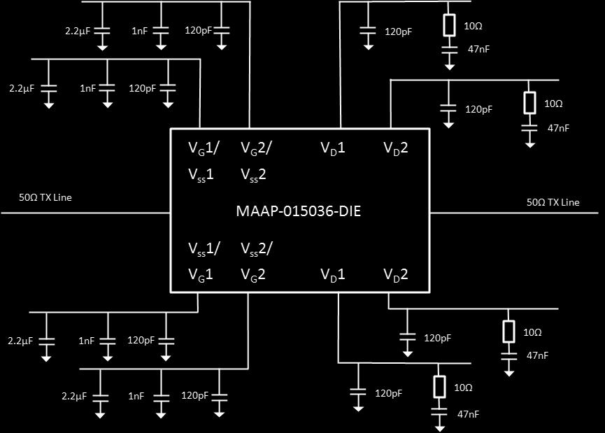
1 Features 15 W Power Amplifier 42 dbm Saturated Pulsed Output Power 17 db Large Signal Gain P SAT >40% Power Added Efficiency Dual Sided Bias Architecture On Chip Bias Circuit 100% On-Wafer DC, RF and Output Power Testing 100% Visual Inspection to MIL-STD-883 Method 2010 Functional Schematic Description The MAAP is a two stage GaAs MMIC power amplifier operating from GHz, with a saturated pulsed output power of 42 dbm and a large signal gain of 18 db. This power amplifier uses GaAs phemt device technology and is based upon optical gate lithography to ensure high repeatability and uniformity. The chip has surface passivation for protection and backside via holes and gold metallisation to allow a conductive epoxy die attach process. This device is well suited for communications, Point to Point radio and radar applications. Pin Configuration 2 1 V G 1 15 V D 2 2 GND 16 GND 3 V SS 1 17 GND 4 V 1_5 18 V D 1 5 GND 19 V G 2 6 V SS 2 20 GND 7 V 2_5 21 V 2_5 8 GND 22 V SS 2 Ordering Information 9 V G 2 23 GND 10 V D 1 24 V 1_5 MAAP DIE Die in Gel Pack 1 MAAP DIEEV1 MAAP DIEEV2 1. Die quantity varies. Sample Board Direct Gate Bias Sample Board On-Chip Gate Bias 11 GND 25 V SS 1 12 GND 26 GND 13 V D 2 27 V G 1 14 RF OUT 28 RF IN 2. Backside metal is RF, DC and thermal ground. 1 * Restrictions on Hazardous Substances, European Union Directive 2011/65/EU.
2 Electrical Specifications - Pulsed Operation: Duty Cycle = 5%, Pulse = 5 µs, Freq. = GHz, T A = +25 C, Z 0 = 50 Ω,, P IN = 26 dbm, V G = -0.9 V Gain (Large Signal) db 17 Gain db 17 Gain Flatness db 1 Input Return Loss db -15 Output Return Loss db -25 Saturated Output Power ( GHz) Saturated Output Power ( GHz) dbm Power Added Efficiency GHz GHz GHz % Drain Bias Voltage V 8.0 Drain Current A Absolute Maximum Ratings 3,4 Input Power Drain Voltage Gate Voltage Bias Voltage Drain Current Gate Current (Direct Bias) Gate Current (On Chip Bias) Operating Temperature Junction Temperature 5,6 30 dbm +8.5 V -3.0 V < V G < -0.0 V -6.0 V < V SS < -4.0 V 6 A 160 ma 165 ma -40 C to +85 C +170 C Handling Procedures Please observe the following precautions to avoid damage: Static Sensitivity These electronic devices are sensitive to electrostatic discharge (ESD) and can be damaged by static electricity. Proper ESD control techniques should be used when handling these HBM Class 1A devices. 3. Exceeding any one or combination of these limits may cause permanent damage to this device. 4. MACOM does not recommend sustained operation near these survivability limits. 5. Operating at nominal conditions with T J +160 C will ensure MTTF > 1.0 x 10 6 hours. 6. Typical thermal resistance (Өjc) = 5.7 C/W. 2
3 Bonding Diagram - On Chip Bias 7 Bonding Diagram - Direct Gate Bias 7 7. Components C1 - C8 are all 120 pf chips. MMIC Bare Die 3


4 Pulsed Performance Curves over Gate Voltage: V D = 8 V, Duty Cycle = 5%, Pulse = 5 µs Gain vs. Frequency Reverse Isolation vs. Frequency Input Return Loss vs. Frequency Output Return Loss vs. Frequency 4

5 Pulsed Performance Curves over Gate Voltage: P IN = 25 dbm, Duty Cycle = 5%, Pulse = 5 µs Gain vs. Frequency Output Power vs. Frequency Drain Current vs. Frequency PAE vs. Frequency 5


6 Pulsed Performance Curves over Freq.: V G = -0.9 V, Duty Cycle = 5%, Pulse = 5 µs Gain vs. Input Power Output Power vs. Input Power Drain Current vs. Input Power PAE vs. Input Power Gate Current vs. Input 9 GHz 6

7 Pulsed Performance Curves over Temperature: V G = -0.9 V, P IN = 25 dbm, Duty Cycle = 5%, Pulse = 5 µs Gain vs. Frequency Output Power vs. Frequency Drain Current vs. Frequency PAE vs. Frequency 7


8 Pulsed Performance Curves over Bias Circuit Voltage, Duty Cycle = 5%, Pulse = 5 µs Gain vs. Frequency Reverse Isolation vs. Frequency Input Return Loss vs. Frequency Output Return Loss vs. Frequency 8


9 Pulsed Performance Curves over Bias Circuit Voltage : P IN = 25 dbm, Duty Cycle = 5%, Pulse = 5 µs Gain vs. Frequency Output Power vs. Frequency Drain Current vs. Frequency PAE vs. Frequency 9


10 Pulsed Performance Curves over Frequency: Bias Circuit Voltage = -5 V, Duty Cycle = 5%, Pulse = 5 µs Gain vs. Input Power Output Power vs. Input Power Drain Current vs. Input Power PAE vs. Input Power Bias Circuit Current vs. Input Power 10
11 Applications Section Application Notes Note 1 - Biasing The gate bias is applied in one of the following: 1. Direct Gate Bias:- V G 1 & V G 2 provide the direct gate bias input to the 2 MMIC stages. This method of biasing allows the user to control the total drain current without the scaling factor provided by the bias circuit. It is recommended that the gate voltage is supplied by both sides of the die. Biasing from one side is optional. Optimum performance can be achieved with a -0.9 V operation. 2. Bias Circuit Biasing:- Applying -5 V to V SS 1 & V SS 2, will typically draw 4.5 A with no further adjustment necessary. Wafer lot variation may result in some devices experiencing higher or lower drain currents than the typical 4.5 A. It is recommended that the bias circuits on both sides of the PA are used. Biasing from one side is optional. Note 4 - Pulse Operation The performance of the MAAP is characterized under pulsed conditions with a duty cycle of 5% consisting of a pulse width of 5 µs applied to the drain. Under pulsed conditions the gate is constantly biased using either the on chip bias circuit or using a gate voltage directly applied to the PA. It is recommended that the die is mounted with an adequate thermal solution. Note 5 - Input / Output Transitions The PA performance must be achieved in a 50 Ω impedance environment on the RF input and output. To maintain performance three bond wires are recommended on the output of the PA each with a maximum length of less than 600 µm. Longer bond wire lengths can be used providing bond pad compensation, in the form of a stub, is used on the application board. Note 2 - Bias Sequence When switching on the PA, In each case, the gate bias must be applied before the drain voltage is applied. The drain voltage V D 1 & V D 2 should be biased from the top and bottom sides of the die. Note 3 - Decoupling Circuits Each bias pad, V G, V SS & V D must have a decoupling capacitor of 120 pf as close to the device as possible, as is shown in the bonding diagrams. Symmetrical decoupling circuits must be maintained on both sides of the die for bias circuit or direct gate bias operation. Under pulsed operation a large capacitance on the drain will cause a ringing effect on the supply voltage. This potentially produces a high voltage at the PA terminals. A recommended decoupling circuit is provided where shunt decoupling capacitors are connected in series with a resistor to minimize this effect. 11
12 Application Circuit 12
13 Applications Section Handling and Assembly Die Attachment This product is manufactured from mm (0.004") thick substrate and has vias through to the backside to enable grounding to the circuit. Microstrip substrates should be brought as close to the die as possible and bond wire lengths on the input and output kept as short as possible. The mounting surface should be clean and flat. If using conductive epoxy, recommended epoxies are Tanaka TS3332LD, Die Mat DM6030HK, Abletherm 2600AT or DM6030HK-Pt cured per the manufacturer's cure schedule. Epoxy should be applied in accordance with the manufacturers specifications and should avoid contact with the top surface of the die. An epoxy fillet should be visible around the total die periphery. For additional information please see the MACOM "Epoxy Specifications for Bare Die" application note. Wire Bonding Windows are provided in the surface passivation above the bond pads to allow wire bonding to the die's gold bond pads. The recommended wire bonding procedure uses mm x mm (0.003" x ") 99.99% pure gold ribbon with 0.5-2% elongation to minimize RF port bond inductance. Gold mm (0.001") diameter wedge or ball bonds are acceptable for DC Bias connections. Aluminium wire should be avoided. Thermo-compression bonding is recommended though thermo-sonic bonding may be used providing the ultrasonic content of the bond is minimized. Bond force, time and ultrasonic's are all critical parameters. Bonds should be made from the bond pads on the die to the package or substrate. All bonds should be as short as possible. If eutectic mounting is preferred, then a flux-less gold-tin (AuSn) preform, approximately thick, placed between the die and the attachment surface should be used. A die attach bonder that utilizes a heated collet and provides scrubbing action to ensure total wetting to prevent void formation in a nitrogen atmosphere is recommended. The gold-tin eutectic (80% Au 20% Sn) has a melting point of approximately 280ºC (Note: Gold Germanium should be avoided). The work station temperature should be 310ºC +/-10ºC. Exposure time to these extreme temperatures should be kept to minimum. The die and collet should be pre-heated, to avoid excessive thermal shock during assembly. Avoidance of air bridges and force impact are critical during placement. 13
GHz GaAs MMIC Power Amplifier
 17.0.0 GHz GaAs MMIC August 07 Rev 08Aug07 Features Excellent Saturated Output Stage Competitive RF/DC Bias Pin for Pin Replacement.0 Small Signal Gain +.0 m Saturated Output Power 0% OnWafer RF, DC and
Electrical Characteristics (Ambient Temperature T = 25 o C) Units GHz db db db db db dbm dbm VDC VDC ma
 Units GHz db db db db db dbm dbm VDC VDC ma") Features Excellent Linear Output Amplifier Stage 21.0 Small Signal Gain +36.0 m Third Order Intercept (OIP3) +27.0 m Output P1 Compression Point 100% OnWafer RF, DC and Output Power Testing 100% Visual
Features Excellent Linear Output Amplifier Stage 21.0 Small Signal Gain +36.0 m Third Order Intercept (OIP3) +27.0 m Output P1 Compression Point 100% OnWafer RF, DC and Output Power Testing 100% Visual
GHz GaAs MMIC Image Reject Mixer
 34.46. GHz GaAs MMIC July 27 Rev 2Jul7 M12BD Features Fundamental 7. Conversion Loss 2. Image Rejection +24 m Input Third Order Intercept 1% OnWafer RF Testing 1% Visual Inspection to MILSTD883 Method
GHz GaAs MMIC Power Amplifier
 Features Excellent Driver Stage. Small Signal Gain +4. m P Compression Point % OnWafer RF, DC and Output Power Testing % Visual Inspection to MILSTD Method Chip Device Layout X General Description Mimix
8 11 GHz 1 Watt Power Amplifier
 Rev. 1.1 December 2 GHz 1 Watt Power Amplifier Features Frequency Range : GHz 3 dbm output P1dB. db Power gain 3% PAE High IP3 Input Return Loss > db Output Return Loss > db Dual bias operation No external
81 GHz to 86 GHz, E-Band Power Amplifier With Power Detector HMC8142
 Data Sheet 8 GHz to 86 GHz, E-Band Power Amplifier With Power Detector FEATURES GENERAL DESCRIPTION Gain: db typical The is an integrated E-band gallium arsenide (GaAs), Output power for db compression
FEATURES DESCRIPTION ABSOLUTE MAXIMUM RATINGS. T AMB = +25 C ( Unless otherwise specified )
") Monolithic PIN SP5T Diode Switch FEATURES Ultra Broad Bandwidth: 50MHz to 26GHz 1.0 db Insertion Loss 30 db Isolation at 20GHz Reliable. Fully Monolithic Glass Encapsulated Construction DESCRIPTION The
Monolithic PIN SP5T Diode Switch FEATURES Ultra Broad Bandwidth: 50MHz to 26GHz 1.0 db Insertion Loss 30 db Isolation at 20GHz Reliable. Fully Monolithic Glass Encapsulated Construction DESCRIPTION The
GHz GaAs MMIC Power Amplifier
 37.042.0 GHz GaAs MMIC February 2007 Rev 01Feb07 P1018BD Features Excellent Transmit Output Stage Output Power Adjust 26.0 Small Signal Gain +25.0 m P1 Compression Point 100% OnWafer RF, DC and Output
MAAP Preliminary Information. Power Amplifier GHz. Preliminary - Rev. V2P. Features. Functional Schematic.
 MAAP-11199 8-1 GHz Features Saturated Output Power: 24 dbm Gain: 12 db Input Return Loss: >1 db Output Return Loss: >1 db Reverse Isolation: >3 db Dimension: 18 x 2 µm 2 RoHS* Compliant Bare Die Functional
Features. = +25 C, Vdd = 5V, Idd = 85mA*
 Typical Applications The is ideal for use as a medium power amplifier for: Point-to-Point and Point-to-Multi-Point Radios VSAT Functional Diagram Features Saturated Power: +23 dbm @ 25% PAE Gain: 15 db
GHz GaAs MMIC Power Amplifier
 17.24. GHz GaAs MMIC May 25 Rev 5May5 Features High Linearity Output Amplifier Balanced Design Provides Good Input/Output Match OnChip Temperature Compensated Output Power Detector 19. Small Signal Gain
5 6 GHz 10 Watt Power Amplifier
 5 6 GHz 10 Watt Power Amplifier Features Frequency Range : 5 6GHz 40 dbm Output Power 18 db Power gain 30% PAE High IP3 Input Return Loss > 12 db Output Return Loss > 7.5 db Dual bias operation No external
Features OBSOLETE. Output Third Order Intercept (IP3) [2] dbm Total Supply Current ma
![Features OBSOLETE. Output Third Order Intercept (IP3) [2] dbm Total Supply Current ma](/thumbs/89/98911879.jpg "Features OBSOLETE. Output Third Order Intercept (IP3) [2] dbm Total Supply Current ma") v.1111 Typical Applications Features The is ideal for: Point-to-Point Radios Point-to-Multi-Point Radios VSAT & SATCOM Military & Space Functional Diagram P1dB Output Power: + dbm Psat Output Power: +
v.1111 Typical Applications Features The is ideal for: Point-to-Point Radios Point-to-Multi-Point Radios VSAT & SATCOM Military & Space Functional Diagram P1dB Output Power: + dbm Psat Output Power: +
Features. = +25 C, Vdd = Vdd1 = Vdd2 = Vdd3 = Vdd4 = Vdd5 = +7V, Idd = 1200mA [1]
![Features. = +25 C, Vdd = Vdd1 = Vdd2 = Vdd3 = Vdd4 = Vdd5 = +7V, Idd = 1200mA [1]](/thumbs/92/108090400.jpg "Features. = +25 C, Vdd = Vdd1 = Vdd2 = Vdd3 = Vdd4 = Vdd5 = +7V, Idd = 1200mA [1]") v2.211 HMC949 Typical Applications The HMC949 is ideal for: Point-to-Point Radios Point-to-Multi-Point Radios VSAT & SATCOM Military & Space Functional Diagram Features Saturated Output Power: +5.5 dbm
v2.211 HMC949 Typical Applications The HMC949 is ideal for: Point-to-Point Radios Point-to-Multi-Point Radios VSAT & SATCOM Military & Space Functional Diagram Features Saturated Output Power: +5.5 dbm
11-15 GHz 0.5 Watt Power Amplifier
 11-15 GHz 0.5 Watt Power Amplifier Features Frequency Range : 11-15GHz 27.5 dbm output Psat 13 db Power gain 25% PAE High IP3 Input Return Loss > 11 db Output Return Loss > 6 db Dual bias operation No
71 GHz to 76 GHz, 1 W E-Band Power Amplifier with Power Detector ADMV7710
 FEATURES Gain: db typical Output power for db compression: dbm typical Saturated output power: 29 dbm typical Output third-order intercept: dbm typical Input return loss: 8 db typical Output return loss:
Features. = +25 C, Vdd1, Vdd2 = +5V
 v.11 HMC51 POWER AMPLIFIER, 5-2 GHz Typical Applications Features The HMC51 is ideal for use as a driver amplifier for: Point-to-Point Radios Point-to-Multi-Point Radios & VSAT Test Equipment & Sensors
71 GHz to 76 GHz, 1 W E-Band Power Amplifier with Power Detector ADMV7710
 Data Sheet FEATURES Gain: db typical Output power for db compression: dbm typical Saturated output power: 29 dbm typical Output third-order intercept: dbm typical Input return loss: 8 db typical Output
Features. DC - 2 GHz GHz Supply Current (Idd) 400 ma
 400 ma") Typical Applications The HMC637A is ideal for: Telecom Infrastructure Microwave Radio & VSAT Military & Space Test Instrumentation Fiber Optics Functional Diagram Features P1dB Output Power: +3.5 dbm Gain:
Typical Applications The HMC637A is ideal for: Telecom Infrastructure Microwave Radio & VSAT Military & Space Test Instrumentation Fiber Optics Functional Diagram Features P1dB Output Power: +3.5 dbm Gain:
GHz GaAs MMIC Power Amplifier
 17.24. GHz GaAs MMIC October 28 Rev 1Oct8 P119BD Features Excellent Transmit Output Stage Temperature Compensated Output Detector 18. Small Signal Gain +27. m P1 Compression Point 1% OnWafer RF, DC and
9-10 GHz LOW NOISE AMPLIFIER
 9-10 GHz LOW NOISE AMPLIFIER Features Frequency Range 9-10GHz Low Noise Figure < 1.38 db High Gain 28 ± 0.4dB Input Return Loss > 10dB. Output Return Loss > 13dB. 10 dbm is Nominal P1dB 20 dbm OIP3 No
Features. = +25 C Vdd = Vdd1, Vdd2, Vdd3, Vdd4, Vdd5, Vdd6, Vdd7, Vdd8 = +6V, Idd = 1400 ma [1]
![Features. = +25 C Vdd = Vdd1, Vdd2, Vdd3, Vdd4, Vdd5, Vdd6, Vdd7, Vdd8 = +6V, Idd = 1400 ma [1]](/thumbs/82/85923909.jpg "Features. = +25 C Vdd = Vdd1, Vdd2, Vdd3, Vdd4, Vdd5, Vdd6, Vdd7, Vdd8 = +6V, Idd = 1400 ma [1]") HMC129 v1.412 Typical Applications The HMC129 is ideal for: Features Saturated Output Power: + dbm @ 25% PAE Point-to-Point Radios Point-to-Multi-Point Radios VSAT & SATCOM Military & Space Functional
HMC129 v1.412 Typical Applications The HMC129 is ideal for: Features Saturated Output Power: + dbm @ 25% PAE Point-to-Point Radios Point-to-Multi-Point Radios VSAT & SATCOM Military & Space Functional
Features. = +25 C, Vdd = 5V, Idd = 200 ma*
 v3.13 HMC9 Typical Applications The HMC9 is ideal for use as either a LNA or driver amplifier for: Point-to-Point Radios Point-to-Multi-Point Radios VSAT Military & Space Functional Diagram Features Noise
Customised Pack Sizes / Qtys. Support for all industry recognised supply formats: o o o. Waffle Pack Gel Pak Tape & Reel
 Design Assistance Assembly Assistance Die handling consultancy Hi-Rel die qualification Hot & Cold die probing Electrical test & trimming Customised Pack Sizes / Qtys Support for all industry recognised
Features. = +25 C, Vdd 1, 2, 3 = +3V
 v3.917 Typical Applications Features The HMC17 is ideal for use as a LNA or Driver amplifier for: Point-to-Point Radios Point-to-Multi-Point Radios & VSAT Test Equipment and Sensors Military & Space Functional
Features. Noise Figure db Supply Current (Idd) ma Supply Voltage (Vdd) V
 ma Supply Voltage (Vdd) V") v2.418 Typical Applications The HMC797A is ideal for: Test Instrumentation Military & Space Fiber Optics Functional Diagram Features High P1dB Output Power: +29 dbm High Psat Output Power: +31 dbm High
v2.418 Typical Applications The HMC797A is ideal for: Test Instrumentation Military & Space Fiber Optics Functional Diagram Features High P1dB Output Power: +29 dbm High Psat Output Power: +31 dbm High
HMC985A. attenuators - analog - Chip. GaAs MMIC VOLTAGE - VARIABLE ATTENUATOR, GHz. Features. Typical Applications. General Description
 Typical Applications The is ideal for: Point-to-Point Radio VSAT Radio Test Instrumentation Microwave Sensors Military, ECM & Radar Functional Diagram v2.917 ATTENUATOR, 2-5 GHz Features Wide Bandwidth:
Features. = +25 C, Vdd = +5V, Idd = 63 ma
 v2.213 LOW NOISE AMPLIFIER, 2-2 GHz Typical Applications Features The is ideal for: Test Instrumentation Microwave Radio & VSAT Military & Space Telecom Infrastructure Fiber Optics Functional Diagram Noise
Features. = +25 C, Vdd= 5V, Idd= 60 ma*
 Typical Applications The HMC63 is ideal for: Telecom Infrastructure Microwave Radio & VSAT Military & Space Test Instrumentation Fiber Optics Functional Diagram v.67 Vgg2: Optional Gate Bias for AGC HMC63
HMC998. Amplifiers - Linear & Power - Chip. GaAs phemt MMIC 2 WATT POWER AMPLIFIER, GHz. Electrical Specifications, T A.
 v1.811 2 WATT POWER AMPLIFIER,.1-22 GHz Typical Applications Features The is ideal for: Test Instrumentation Microwave Radio & VSAT Military & Space Telecom Infrastructure Fiber Optics Functional Diagram
Features. = +25 C, Vdd 1, 2, 3 = +3V
 v.91 HMC519 AMPLIFIER, 1-32 GHz Typical Applications The HMC519 is ideal for use as either a LNA or driver amplifier for: Point-to-Point Radios Point-to-Multi-Point Radios & VSAT Test Equipment & Sensors
8-18 GHz Wideband Low Noise Amplifier
 8-18 GHz Wideband Low Noise Amplifier Features Frequency Range : 8.0 18.0GHz 23dB Nominal gain Low Midband Noise Figure < 2 db Input Return Loss > 12 db Output Return Loss > 12 db Single +3V Operation
Features. = +25 C, With 0/-5V Control, 50 Ohm System
 Typical Applications This switch is suitable DC - 0 GHz applications: Fiber Optics Microwave Radio Military Space VSAT Functional Diagram Features High Isolation: >40 db @ 0 GHz Low Insertion Loss:.1 db
Features. = +25 C, With 0/-5V Control, 50 Ohm System
 Typical Applications This switch is suitable 0.1-0 GHz applications: Fiber Optics Microwave Radio Military Space VSAT Functional Diagram Features High Isolation: 45 db @ 0 GHz Low Insertion Loss: 1.7 db
5 6.4 GHz 2 Watt Power Amplifier
 5 6.4 GHz 2 Watt Power Amplifier Features Frequency Range : 5 6.4GHz 32.5 dbm output P1dB 9 db Power gain 32% PAE High IP3 Input Return Loss > 12 db Output Return Loss > 12 db Dual bias operation No external
HMC906A. Amplifiers - Linear & Power - CHIP. Electrical Specifications, T A. Typical Applications. Features. General Description. Functional Diagram
 Typical Applications Features The HMC96A is ideal for: Satellite Communications Point-to-Point Radios Point-to-Multi-Point Radios VSAT Military & Space Functional Diagram Saturated Output Power: +33.5
Features. = +25 C, Vdd = +6V, Idd = 375mA [1]
![Features. = +25 C, Vdd = +6V, Idd = 375mA [1]](/thumbs/86/94452749.jpg "Features. = +25 C, Vdd = +6V, Idd = 375mA [1]") v.119 HMC86 POWER AMPLIFIER, 24 -.5 GHz Typical Applications The HMC86 is ideal for: Point-to-Point Radios Point-to-Multi-Point Radios VSAT Military & Space Functional Diagram Features Saturated Output
v.119 HMC86 POWER AMPLIFIER, 24 -.5 GHz Typical Applications The HMC86 is ideal for: Point-to-Point Radios Point-to-Multi-Point Radios VSAT Military & Space Functional Diagram Features Saturated Output
Features OUT E S T CODE. = +25 C, Vdd= 8V, Idd= 60 ma*
 E S T CODE E S T CODE v1.818 HMC6 AMPLIFIER, DC - 2 GHz Typical Applications Features The HMC6 is ideal for: Noise Figure: 2.5 db @ 1 GHz Telecom Infrastructure Microwave Radio & VSAT Military & Space
Features. = +25 C, Vdd= 2V [1], Idd = 55mA [2]
![Features. = +25 C, Vdd= 2V [1], Idd = 55mA [2]](/thumbs/89/100957500.jpg "Features. = +25 C, Vdd= 2V [1], Idd = 55mA [2]") HMC-ALH12 Typical Applications This HMC-ALH12 is ideal for: Features Noise Figure: 2.5 db Wideband Communications Receivers Surveillance Systems Point-to-Point Radios Point-to-Multi-Point Radios Military
HMC-ALH12 Typical Applications This HMC-ALH12 is ideal for: Features Noise Figure: 2.5 db Wideband Communications Receivers Surveillance Systems Point-to-Point Radios Point-to-Multi-Point Radios Military
Features dbm
 v9.917 HMC441 Typical Applications Features The HMC441 is ideal for: Point-to-Point and Point-to-Multi-Point Radios VSAT LO Driver for HMC Mixers Military EW & ECM Functional Diagram Gain:.5 db Saturated
2 GHz to 30 GHz, GaAs, phemt, MMIC, Low Noise Amplifier HMC8402
 2 GHz to 3 GHz, GaAs, phemt, MMIC, Low Noise Amplifier HMC842 FEATURES Output power for 1 db compression (P1dB): 21. dbm typical Saturated output power (PSAT): 22 dbm typical Gain: 13. db typical Noise
14 GHz to 32 GHz, GaAs, MMIC, Double Balanced Mixer HMC292A
 14 GHz to 32 GHz, GaAs, MMIC, Double Balanced Mixer FEATURES Passive: no dc bias required Conversion loss (downconverter): 9 db typical at 14 GHz to 3 GHz Single-sideband noise figure: 11 db typical at
Features. = +25 C, Vdd 1, 2, 3 = +3V
 Typical Applications Functional Diagram v2.29 The HMC6 is ideal for use as a LNA or driver amplifi er for : Point-to-Point Radios Point-to-Multi-Point Radios & VSAT Test Equipment and Sensors Military
HMC994A AMPLIFIERS - LINEAR & POWER - CHIP. GaAs phemt MMIC 0.5 WATT POWER AMPLIFIER, DC - 30 GHz. Features. Typical Applications
 v3.218 HMC994A.5 WATT POWER AMPLIFIER, DC - 3 GHz Typical Applications The HMC994A is ideal for: Test Instrumentation Military & Space Fiber Optics Functional Diagram Features High P1dB Output Power: dbm
Features. = +25 C, Vdd 1, 2, 3 = +3V
 Typical Applications Functional Diagram v.97 The HMC is ideal for use as a LNA or driver amplifi er for : Point-to-Point Radios Point-to-Multi-Point Radios & VSAT Test Equipment and Sensors Military &
MAAL DIESMB. Low Noise Amplifier DC - 28 GHz. Features. Functional Schematic 1. Description. Pin Configuration 2. Ordering Information. Rev.
 MAAL-11141-DIE Features Ultra Wideband Performance Noise Figure: 1.4 db @ 8 GHz High Gain: 17 db @ 8 GHz Output IP3: 28 dbm @ 8 GHz Bias Voltage: V DD = - V Bias Current: I DSQ = 6 - ma Ω Matched Input
Features. = +25 C, Vdd = +10V, Idd = 350mA
 Typical Applications The is ideal for: Test Instrumentation Military & Space Functional Diagram Features High P1dB Output Power: +28 dbm High : 14 db High Output IP3: +41 dbm Single Supply: +V @ 3 ma Ohm
HMC-APH596 LINEAR & POWER AMPLIFIERS - CHIP. GaAs HEMT MMIC MEDIUM POWER AMPLIFIER, GHz. Typical Applications. Features
 Typical Applications Features This is ideal for: Point-to-Point Radios Point-to-Multi-Point Radios VSAT Military & Space Functional Diagram Output IP: + dbm P1dB: +24 dbm Gain: 17 db Supply Voltage: +5V
Features. = +25 C, Vdd= +8V *
 Typical Applications Features This is ideal for: Fiber Optic Modulator Driver Fiber Optic Photoreceiver Post Amplifi er Gain Block for Test & Measurement Equipment Point-to-Point/Point-to-Multi-Point Radio
DC to 28 GHz, GaAs phemt MMIC Low Noise Amplifier HMC8401
 FEATURES Output power for db compression (PdB):.5 dbm typical Saturated output power (PSAT): 9 dbm typical Gain:.5 db typical Noise figure:.5 db Output third-order intercept (IP3): 26 dbm typical Supply
HMC561 FREQUENCY MULTIPLIER - ACTIVE - CHIP. Electrical Specifications, T A. Features. Typical Applications. General Description. Functional Diagram
 Typical Applications The HMC51 is suitable for: Clock Generation Applications: SONET OC-19 & SDH STM- Point-to-Point & VSAT Radios Test Instrumentation Military & Space Functional Diagram Features High
Features. The HMC985 is ideal for: = +25 C, See Test Conditions. Parameter Condition Min. Typ. Max. Units db. Output Return Loss 13 db
 Typical Applications The is ideal for: Point-to-Point Radio Vsat Radio Test Instrumentation Microwave Sensors Military, ECM & Radar Functional Diagram v.211 attenuator, 2-5 GHz Features Wide Bandwidth:
Features. = +25 C, Vdd = +3V
 v.117 HMC Typical Applications Features The HMC is ideal for: Millimeterwave Point-to-Point Radios LMDS VSAT SATCOM Functional Diagram Excellent Noise Figure: db Gain: db Single Supply: +V @ 8 ma Small
Features. = 25 C, IF = 3 GHz, LO = +16 dbm
 mixers - i/q mixers / irm - CHIP Typical Applications This is ideal for: Point-to-Point Radios Test & Measurement Equipment SATCOM Radar Functional Diagram Features Wide IF Bandwidth: DC - 5 GHz High Image
Features. = +25 C, Vdd= +5V
 Typical Applications This is ideal for: Wideband Communication Systems Surveillance Systems Point-to-Point Radios Point-to-Multi-Point Radios Military & Space Test Instrumentation * VSAT Functional Diagram
50 GHz to 95 GHz, GaAs, phemt, MMIC, Wideband Power Amplifier ADPA7001CHIPS
 FEATURES Gain:.5 db typical at 5 GHz to 7 GHz S11: db typical at 5 GHz to 7 GHz S: 19 db typical at 5 GHz to 7 GHz P1dB: 17 dbm typical at 5 GHz to 7 GHz PSAT: 1 dbm typical OIP3: 5 dbm typical at 7 GHz
Features. Output Third Order Intercept (IP3) [2] dbm Power Added Efficiency %
![Features. Output Third Order Intercept (IP3) [2] dbm Power Added Efficiency %](/thumbs/84/89186722.jpg "Features. Output Third Order Intercept (IP3) [2] dbm Power Added Efficiency %") v5.1217 HMC187 2-2 GHz Typical Applications The HMC187 is ideal for: Test Instrumentation General Communications Radar Functional Diagram Features High Psat: +39 dbm Power Gain at Psat: +5.5 db High Output
v5.1217 HMC187 2-2 GHz Typical Applications The HMC187 is ideal for: Test Instrumentation General Communications Radar Functional Diagram Features High Psat: +39 dbm Power Gain at Psat: +5.5 db High Output
Features OBSOLETE. = +25 C, With 0/-5V Control, 50 Ohm System. DC - 10 GHz DC - 6 GHz DC - 15 GHz. DC - 6 GHz DC - 15 GHz
 v03.1203 Typical Applications Broadband switch for applications: Fiber Optics Microwave Radio Military & Space Test Equipment VSAT Functional Diagram Features High Isolation: >50 @ 10 GHz Low Insertion
HMC-AUH232 MICROWAVE & OPTICAL DRIVER AMPLIFIERS - CHIP. GaAs HEMT MMIC MODULATOR DRIVER AMPLIFIER, DC - 43 GHz. Typical Applications.
 DRIVER AMPLIFIER, DC - 3 GHz Typical Applications This is ideal for: 0 Gb/s Lithium Niobate/ Mach Zender Fiber Optic Modulators Broadband Gain Block for Test & Measurement Equipment Broadband Gain Block
GaAs, phemt, MMIC, Power Amplifier, HMC1126. Data Sheet FEATURES FUNCTIONAL BLOCK DIAGRAM APPLICATIONS GENERAL DESCRIPTION
 Data Sheet GaAs, phemt, MMIC, Power Amplifier, GHz to GHz FEATURES FUNCTIONAL BLOCK DIAGRAM Output power for 1 db compression (P1dB): 1. db typical Saturated output power (PSAT): 1 dbm typical Gain: 11
HMC465 AMPLIFIERS- DRIVERS & GAIN BLOCKS - CHIP. GaAs phemt MMIC MODULATOR DRIVER AMPLIFIER, DC - 20 GHz. Electrical Specifications, T A.
 v9.114 DRIVER AMPLIFIER, DC - 2 GHz Typical Applications The wideband driver is ideal for: OC192 LN/MZ Modulator Driver Telecom Infrastructure Test Instrumentation Military & Space Functional Diagram Features
Features. = +25 C, Vdd = 5V
 v1.1 AMPLIFIER, 3. - 7. GHz Typical Applications The HMC39A is ideal for: Point-to-Point Radios VSAT LO Driver for HMC Mixers Military EW, ECM, C 3 I Space Functional Diagram Features Gain: 17. db Noise
GaAs phemt MMIC Low Noise Amplifier, 0.3 GHz to 20 GHz HMC1049
 Data Sheet GaAs phemt MMIC Low Noise Amplifier,. GHz to GHz HMC9 FEATURES FUNCTIONAL BLOCK DIAGRAM Low noise figure:.7 db High gain: 6 db PdB output power: dbm Supply voltage: 7 V at 7 ma Output IP: 7
XZ1002-BD GHz GaAs MMIC Core Chip
 XZ2BD.5. GHz GaAs MMIC Rev Sep Features Highly Integrated Transmit and Receive Modes of Operation Integrated T/R Switches, LNA and Driver Amplifier, 6Bit Phase Shifter and 5Bit Attenuator 2. Small Signal
Features. = +25 C, Vdd 1, 2, 3, 4 = +3V
 Typical Applications Functional Diagram v.3 The HMC5 is ideal for use as a LNA or driver amplifi er for: Point-to-Point Radios Point-to-Multi-Point Radios & VSAT Test Equipment and Sensors Military & Space
71 GHz to 76 GHz, E-Band Variable Gain Amplifier HMC8120
 Data Sheet FEATURES Gain: 22 db typical Wide gain control range: 1 db typical Output third-order intercept (OIP3): 3 dbm typical Output power for 1 db compression (P1dB): 21 dbm typical Saturated output
2 40 GHz Ultra-Wideband Amplifier
 AMT217511 Rev. 1. January 28 2 4 GHz Ultra-Wideband Amplifier Features Frequency Range: 2-4 GHz 7±1. db Nominal Gain Input Return Loss > 1 db Output Return Loss > 1 db Reverse Isolation > 3dB 5 dbm Nominal
HMC576 FREQUENCY MULTIPLIERS - ACTIVE - CHIP. GaAs MMIC x2 ACTIVE FREQUENCY MULTIPLIER, GHz OUTPUT. Features. Typical Applications
 v.56 GaAs MMIC x ACTIVE FREQUENCY MULTIPLIER, 18-9 GHz OUTPUT Typical Applications The is suitable for: Clock Generation Applications: SONET OC-19 & SDH STM-64 Point-to-Point & VSAT Radios Test Instrumentation
Customised Pack Sizes / Qtys. Support for all industry recognised supply formats: o o o. Waffle Pack Gel Pak Tape & Reel
 Design Assistance Assembly Assistance Die handling consultancy Hi-Rel die qualification Hot & Cold die probing Electrical test & trimming Customised Pack Sizes / Qtys Support for all industry recognised
Analog Devices Welcomes Hittite Microwave Corporation NO CONTENT ON THE ATTACHED DOCUMENT HAS CHANGED
 Analog Devices Welcomes Hittite Microwave Corporation NO CONTENT ON THE ATTACHED DOCUMENT HAS CHANGED www.analog.com www.hittite.com THIS PAGE INTENTIONALLY LEFT BLANK v0.0907 HMC37 Typical Applications
Data Sheet. AMMC GHz Amplifier. Description. Features. Applications
 AMMC - 518-2 GHz Amplifier Data Sheet Chip Size: 92 x 92 µm (.2 x.2 mils) Chip Size Tolerance: ± 1µm (±.4 mils) Chip Thickness: 1 ± 1µm (4 ±.4 mils) Pad Dimensions: 8 x 8 µm (.1 x.1 mils or larger) Description
DC-12 GHz Tunable Passive Gain Equalizer
 DC-12 GHz Tunable Passive Gain Equalizer AMT1753011 Features Frequency Range : DC-12 GHz 6 db insertion loss Tunable gain slope (+0.5dB/GHz to -0.2 db/ghz) Input Return Loss > 8 db Output Return Loss >
GHz 10 Watt Power Amplifier
 ASL 1 8. 1 GHz 1 Watt Power Amplifier Features Frequency Range : 8. 1GHz. dbm Psat 14 db Power gain 27% PAE High IP3 Input Return Loss > 1 db Output Return Loss > 9 db Dual bias operation DC decoupled
GHz Ultra-wideband Amplifier
 .-3 GHz Ultra-wideband Amplifier Features Frequency Range :. 3.GHz 11. db Nominal gain Gain Flatness: ±2. db Input Return Loss > 1 db Output Return Loss > 1 db DC decoupled input and output.1 µm InGaAs
Features. Gain: 15.5 db. = +25 C, Vdd = 5V
 Typical Applications v2.97 Features AMPLIFIER, 3.5-7. GHz The HMC392 is ideal for: Gain: 5.5 db Point-to-Point Radios VSAT LO Driver for HMC Mixers Military EW, ECM, C 3 I Space Functional Diagram Noise
9-10 GHz GaAs MMIC Core Chip
 9-10 GHz GaAs MMIC Core Chip Features Functional Diagram Frequency Range: 9GHz 10GHz Tx Small Signal Gain: 28dB Rx Small Signal Gain: 4dB Tx Output P1dB : 22dBm Tx Output Psat : 23dBm Input Return Loss
HMC814. GaAs MMIC x2 ACTIVE FREQUENCY MULTIPLIER, GHz OUTPUT. Features. Typical Applications. Functional Diagram. General Description
 v.119 Typical Applications The is ideal for: Clock Generation Applications: SONET OC-19 & SDH STM-64 Point-to-Point & VSAT Radios Test Instrumentation Military & Space Sensors Functional Diagram Features
20 40 GHz Amplifier. Technical Data HMMC-5040
 2 4 GHz Amplifier Technical Data HMMC-4 Features Large Bandwidth: 2-44 GHz Typical - 4 GHz Specified High : db Typical Saturated Output Power: dbm Typical Supply Bias: 4. volts @ 3 ma Description The HMMC-4
Features. = +25 C, Vdd= +5V, Idd = 66mA
 Typical Applications This HMC-ALH369 is ideal for: Features Excellent Noise Figure: 2 db Point-to-Point Radios Point-to-Multi-Point Radios Phased Arrays VSAT SATCOM Functional Diagram Gain: 22 db P1dB
Passive MMIC 30GHz Equalizer
 Page 1 The is a passive MMIC equalizer. It is a positive gain slope equalizer designed to pass DC to 30GHz. Equalization can be applied to reduce low pass filtering effects in both RF/microwave and high
Features. = +25 C, 50 Ohm System
 Typical Applications Features This is ideal for: Low Insertion Loss:.5 db Point-to-Point Radios Point-to-Multi-Point Radios Military Radios, Radar & ECM Test Equipment & Sensors Space Functional Diagram
18-40 GHz Low Noise Amplifier
 18-40 GHz Low Noise Amplifier AMT2172011 Features Frequency Range: 18-40 GHz Better than 4.5 db Noise Figure Single supply operation DC decoupled Input and Output 10 db Nominal Gain 6dBm Nominal P1dB Input
DC-8.0 GHz InGaP HBT MMIC Matched Gain Block Amplifier
 CGB17-BD Features Low Operating Voltage: 5V 33.8 m Output IP3 @ 850 MHz 3.3 Noise Figure @ 850 MHz 23.1 Gain @ 850 MHz, 19.5 @ 6 GHz.2 m P1 @ 850 MHz Low Performance Variation Over Temperature 0% DC On-Wafer
HMC650 TO HMC658 v
 HMC65 TO v1.38 WIDEBAND FIXED ATTENUATOR FAMILY, DC - 5 GHz HMC65 / 651 / 65 / 653 / 654 / 655 / 656 / 657 / 658 Typical Applications The HMC65 through are ideal for: Fiber Optics Microwave Radio Military
HMC-SDD112 SWITCHES - CHIP. GaAs PIN MMIC SPDT SWITCH GHz. Typical Applications. Features. General Description. Functional Diagram
 Typical Applications This is ideal for: FCC E-Band Communication Systems Short-Haul / High Capacity Radios Automotive Radar Test & Measurement Equipment SATCOM Sensors Features Low Insertion Loss: 2 db
Passive MMIC 26-40GHz Bandpass Filter
 Page 1 The is a passive MMIC bandpass filter. It is a low loss integrated filter that passes the Ka (26-40GHz) band. Passive GaAs MMIC technology allows production of smaller filter constructions that
AMMC KHz 40 GHz Traveling Wave Amplifier
 AMMC- 3 KHz GHz Traveling Wave Amplifier Data Sheet Chip Size: Chip Size Tolerance: Chip Thickness: Pad Dimensions: 3 x µm (9. x 1.3 mils) ± µm (±. mils) ± µm ( ±. mils) 8 x 8 µm (.9 ±. mils) Description
GaAs, phemt, MMIC, Power Amplifier, 2 GHz to 50 GHz HMC1126
 GaAs, phemt, MMIC, Power Amplifier, 2 GHz to GHz FEATURES FUNCTIONAL BLOCK DIAGRAM Output power for 1 db compression (P1dB): 1. db typical Saturated output power (PSAT): dbm typical Gain: 11 db typical
Data Sheet. AMMC GHz 0.2 W Driver Amplifier. Features. Description. Applications
 AMMC-6333 18 33 GHz.2 W Driver Amplifier Data Sheet Chip Size: x 13 m (1 x 51 mils) Chip Size Tolerance: ± 1 m (±.4 mils) Chip Thickness: 1 ± 1 m (4 ±.4 mils) Pad Dimensions: 1 x 1 m (4 x 4 ±.4 mils) Description
Features. Parameter Frequency (GHz) Min. Typ. Max. Units. Attenuation Range GHz 31 db. All States db db. 0.
 Min. Typ. Max. Units. Attenuation Range GHz 31 db. All States db db. 0.") Typical Applications The is ideal for: Features 1. LSB Steps to 31 Fiber Optics & Broadband Telecom Microwave Radio & VSAT Military Radios, Radar & ECM Space Applications Functional Diagram 11 3 4 5 6
Typical Applications The is ideal for: Features 1. LSB Steps to 31 Fiber Optics & Broadband Telecom Microwave Radio & VSAT Military Radios, Radar & ECM Space Applications Functional Diagram 11 3 4 5 6
MAAP STD Power Amplifier, 2 W GHz Rev. V2 Features Functional Schematic Description Pin Configuration2 Ordering Information1
 Features 24 db Small Signal Gain 41 dbm Third Order Intercept Point (OIP3) >2 W Output P1dB 35 dbm Saturated Output Power Integrated Power Detector Bias 1330 ma @ 6 V Lead-Free 7 mm Cavity Package RoHS*
20 GHz to 44 GHz, GaAs, phemt, MMIC, Low Noise Amplifier HMC1040CHIPS
 Data Sheet FEATURES Low noise figure: 2 db typical High gain: 25. db typical P1dB output power: 13.5 dbm, 2 GHz to GHz High output IP3: 25.5 dbm typical Die size: 1.39 mm 1..2 mm APPLICATIONS Software
Features. Parameter Frequency Min. Typ. Max. Units GHz GHz GHz GHz GHz GHz
 v1.16 SPDT SWITCH,.1 - GHz Typical Applications The HMC986A is ideal for: Wideband Switching Matrices High Speed Data Infrastructure Military Comms, RADAR, and ECM Test and Measurement Equipment Jamming
HMC397 DRIVER & GAIN BLOCK AMPLIFIERS - CHIP. InGaP HBT GAIN BLOCK MMIC AMPLIFIER, DC - 10 GHz. Features. Typical Applications. General Description
 v3.19 MMIC AMPLIFIER, DC - 1 GHz Typical Applications An excellent cascadable Ohm Block or LO Driver for: Microwave & VSAT Radios Test Equipment Military EW, ECM, C 3 I Space Telecom Functional Diagram
9-10 GHz GaAs MMIC Core Chip
 9-10 GHz GaAs MMIC Core Chip Features Functional Diagram Frequency Range: 9GHz 10GHz Tx Small Signal Gain: 28dB Rx Small Signal Gain: 4dB Tx Output P 1dB : 22dBm Tx Output P sat : 23dBm Input Return Loss
MAAM Wideband Amplifier 10 MHz - 40 GHz Rev. V2. Features. Functional Schematic. Description. Pin Configuration. Ordering Information 1,2
 MAAM-1119 1 MHz - 4 GHz Rev. V2 Features 13 db Gain Ω Input / Output Match +18 dbm Output Power + V DC, 19 ma Lead-Free mm 9-lead LGA Package RoHS* Compliant and 26 C Reflow Compatible Description The
GHz Voltage Variable Attenuator (Absorptive)
") Rev.. February 27.5-2.GHz Voltage Variable Attenuator (Absorptive) Features Single Positive Voltage Control: to +5V. 3dB Attenuation Range Low Insertion Loss I/O VSWR
Rev.. February 27.5-2.GHz Voltage Variable Attenuator (Absorptive) Features Single Positive Voltage Control: to +5V. 3dB Attenuation Range Low Insertion Loss I/O VSWR
Features. = +25 C, LO Drive = +15 dbm* Parameter Min. Typ. Max. Units Frequency Range, RF & LO 4-8 GHz Frequency Range, IF DC - 3 GHz
 v.17 MIXER, - 8 GHz Typical Applications The is ideal for: Microwave & VSAT Radios Test Equipment Military EW, ECM, C 3 I Space Telecom Features Conversion Loss: 7 db LO to RF and IF Isolation: db Input
MA4AGSW2. AlGaAs SP2T PIN Diode Switch. MA4AGSW2 Layout. Features. Description. Absolute Maximum Ratings TA = +25 C (Unless otherwise specified)
") AlGaAs SP2T PIN Diode Switch Features Ultra Broad Bandwidth: 5 MHz to 5 GHz Functional bandwidth : 5 MHz to 7 GHz.7 db Insertion Loss, 33 db Isolation at 5 GHz Low Current consumption: -1 ma for Low Loss
AlGaAs SP2T PIN Diode Switch Features Ultra Broad Bandwidth: 5 MHz to 5 GHz Functional bandwidth : 5 MHz to 7 GHz.7 db Insertion Loss, 33 db Isolation at 5 GHz Low Current consumption: -1 ma for Low Loss
NPA100-D GHz GaN 20W Power Amplifier. Product Description: Key Features:
 Product Description: The Nxbeam is a Ku-band high power GaN MMIC fabricated in 0.2um GaN HEMT on SiC. This part is ideally suited for satellite communications, point-to-point radios, and radar applications.