!"#$"%&' ()#*+,-+.&/0(
|
|
|
- Rosamond Stokes
- 6 years ago
- Views:
Transcription
1 !"#$"%&' ()#*+,-+.&/0(

2 Multi Chip Modules (MCM) or Multi chip packaging Industry s first MCM from IBM. Generally MCMs are horizontal or two-dimensional modules. Defined as a single unit containing two or more chips and an interconnection substrate which function together as a system building block. Need for MCM More functionality in one single chip Special circuit needs met MCMs formed from multiple chips on a IBM s 61-layer LTCC MCM, 1992 common substrate / package structure Do away with individually packaged chips on a PWB ('745869(!57:(;<7(;(,4==<><?(!;#?(%,68@A(
; a complete PC in a MCM possible")
3 Multiple Chip Module (MCM) Increase integration level of system (smaller size) Decrease loading of external signals, hence, higher electrical performance No packaging of individual chips Problems with cooling; special cooling requirements may be required yet Still expensive; but used for high-end applications (eg: military, aerospace etc); a complete PC in a MCM possible ('745869(B2C2=6D2<(#7==7EF(
4 Type of MCMs 1. MCM-Deposited thin film 2. MCM-Ceramic 3. MCM-Laminated organic What are the issues? 1. Feature size 2. Via size 3. Layer count 4. Dielectric constant 5. Dielectric thickness 6. Integrated resistors/ capacitors ('745869(14ED<=6EG<>F(7:(H'!I(;<7(,4==<><(
3%(6&,7(010.1($%/(010.8( P7Q(87FGA(!")
5 Multichip Module: MCM-L!"#$%&'()*+),"$,-).+$)-/(010.2( F( D6=<EDFA( ( 1345$"&)3%(6&,7(010.1($%/(010.8( P7Q(87FGA(!<5<>>6>(:<R528<M7E(L5786FF( &<F6(7:(56L<252E3(7:(56Q75C2E3(2ED2K2D4<>(><O65F( B6>>I6FG<R>2F@6D(2E:5<FG548G456S(R<F6D(7E(!BJ(=<E4:<8G452E3(( "FF6=R>26F(Q2G@(87=L7E6EGF(2E(R7G@(F2D6F( ( 8"$6+$'9:( '23E2T8<EG(#,&(=2F=<G8@(R6GQ66E(F4RFG5<G6(<ED(D26(=<G652<>F( P7Q(L65:75=<E86(<ED(Q252E3(D6EF2GO(!775(G@65=<>(87ED48MK2GO(7:(F4RFG5<G6( H72FG456(F6EF2MK2GO(7:(=<G652<>F( U23@(#57FFG<>C(E72F6

6 Multichip Module: MCM-C ('745869(14ED<=6EG<>F(7:(H'!I(;<7(,4==<><( Ceramic substrate-based MCM-C Substrates based on co-fired ceramic or glass-ceramic technologies. Comparison with MCM-L and MCM-D High wiring density Better electrical and thermal conductivity than MCM-L Assemblies with components on both sides Flexible packaging Superior strength and rigidity Parallel manufacturing process Lower wiring density than MCM-D High dielectric constant (not suitable for high frequencies)
7 Multichip Module: MCM-D Silicon substrate-based MCM-D MCM-D are formed by Deposited dielectrics and conductors on a base substrate typically made with silicon. Comparison with MCM-L and MCM-C Highest performance Highest wiring density Low dielectric constant Good electrical properties Highest cost MCM-L : MCM-C: MCM-D

8 SIP- System in Package System in Package is defined as the vertical stacking of similar or dissimilar ICs, in contrast to the horizontal nature of SOC. Benefits: simpler design, design verification and process besides minimal time-to-market. About 30 IC and packaging companies are producing SIPbased multichip modules. SiP is a key technology for reducing product size and increasing product functionality in products like digital cameras and mobile phones ('745869(14ED<=6EG<>F(7:(H'!I(;<7(,4==<><(
9 SIP- SUMMARY SiP may contain one or more IC chips (wire bonded or flip chip) plus other components that are traditionally found on the system mother board such as: Passive Components: Surface mount discrete passive Integrated passive networks (IPNs) Passives embedded or patterned in the package substrate Other typical components assembled on the system board: SAW / BAW filters EMI Shields Pre-packaged ICs Connectors Mechanical parts The power of SiP is the ability to bring together many IC and package assembly and test technologies to create highly integrated products with optimized cost, size and performance.
 2.")
10 System-on-Package 1. Seamless integration of functional Units (chips) 2. A single-level packaged system
 New Materials (tin, silver, copper) for Die Attach, plating, solder balls SOP, POP (package-on-package)")
11 Current Trends 3D Packaging- Stacked Die Build-Up Substrates Flip-Chip SiP DCA- Direct Chip Attach LTCC, Bluetooth Standard Green Manufacturing Removing Lead (Pb) New Materials (tin, silver, copper) for Die Attach, plating, solder balls SOP, POP (package-on-package) ('745869(B2C2=6D2<(#7==7EF(

12 Road Map for Hand Held Devices ('745869(2+&H-(

13 Road Map for High Performance Systems ('745869(2+&H-(
14 SUMMARY PGAs to BGAs Peripheral array to area array packaging Conventional package footprint to CSP Single chip package to multi chip packaging Packaged chips to flip chip direct chip attach, FC-DCA Mechanically drilled vias to microvias by various technologies Closer integration of packaging hierarchies Environmental aspects in production taken care of Time to volume times drastically reduced
15 Hybrid Circuits Hybrid circuit is one in which either the bare die or a packaged die is mounted on a ceramic substrate and interconnected to on-board passives. Two types of hybrids are known depending on the technology used to build the discrete passives components - Thick Film Hybrids - Thin Film Hybrids
16 Thick Film Hybrids Print and fire technology Inks are used to make conductors, resistors, capacitors. Desired properties are obtained ONLY AFTER FIRING. Conducting Inks For Tracks Resistor Inks - Resistors - trimmed Dielectric Inks To build Capacitors Substrate - Co-fired ceramics
17 Thin Film Hybrids Vacuum deposition technology Vacuum deposition techniques are used to deposit conductors, resistors and dielectrics to build the passive components followed by laser trimming to obtain precise values. HTCC- High temperature Co-fired Ceramics [ 750 C to 1000 C] LTCC Low temperature Co-fired Ceramics [350 C to 600 C]
18 ,.,*;-"P'( V.-W(
19
Sectional Design Standard for High Density Interconnect (HDI) Printed Boards
 Printed Boards") IPC-2226 ASSOCIATION CONNECTING ELECTRONICS INDUSTRIES Sectional Design Standard for High Density Interconnect (HDI) Printed Boards Developed by the HDI Design Subcommittee (D-41) of the HDI Committee
IPC-2226 ASSOCIATION CONNECTING ELECTRONICS INDUSTRIES Sectional Design Standard for High Density Interconnect (HDI) Printed Boards Developed by the HDI Design Subcommittee (D-41) of the HDI Committee
EMERGING SUBSTRATE TECHNOLOGIES FOR PACKAGING
 EMERGING SUBSTRATE TECHNOLOGIES FOR PACKAGING Henry H. Utsunomiya Interconnection Technologies, Inc. Suwa City, Nagano Prefecture, Japan henryutsunomiya@mac.com ABSTRACT This presentation will outline
Benzocyclobutene Polymer dielectric from Dow Chemical used for wafer-level redistribution.
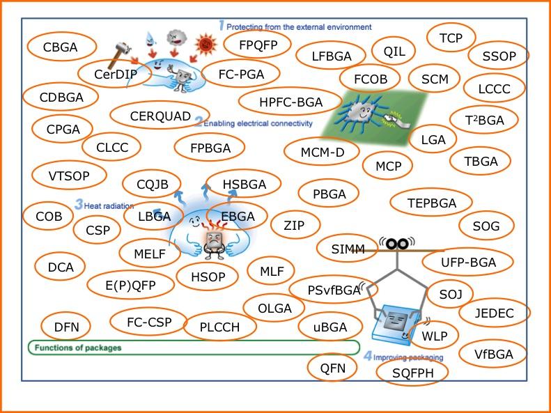
 Glossary of Advanced Packaging: ACA Bare Die BCB BGA BLT BT C4 CBGA CCC CCGA CDIP or CerDIP CLCC COB COF CPGA Anisotropic Conductive Adhesive Adhesive with conducting filler particles where the electrical
David B. Miller Vice President & General Manager September 28, 2005
 Electronic Technologies Business Overview David B. Miller Vice President & General Manager September 28, 2005 Forward Looking Statement During the course of this meeting we may make forward-looking statements.
Thin Film Resistor Integration into Flex-Boards
 Thin Film Resistor Integration into Flex-Boards 7 rd International Workshop Flexible Electronic Systems November 29, 2006, Munich by Dr. Hans Burkard Hightec H MC AG, Lenzburg, Switzerland 1 Content HiCoFlex:
Application Bulletin 240
 Application Bulletin 240 Design Consideration CUSTOM CAPABILITIES Standard PC board fabrication flexibility allows for various component orientations, mounting features, and interconnect schemes. The starting
Silicon Interposers enable high performance capacitors
 Interposers between ICs and package substrates that contain thin film capacitors have been used previously in order to improve circuit performance. However, with the interconnect inductance due to wire
The Future of Packaging ~ Advanced System Integration
 The Future of Packaging ~ Advanced System Integration Enabling a Microelectronic World R. Huemoeller SVP, Adv. Product / Platform Develop June 2013 Product Segments End Market % Share Summary 2 New Product
SiP packaging technology of intelligent sensor module. Tony li
 SiP packaging technology of intelligent sensor module Tony li 2016.9 Contents What we can do with sensors Sensor market trend Challenges of sensor packaging SiP technology to overcome challenges Overview
Chapter 2. Literature Review
 Chapter 2 Literature Review 2.1 Development of Electronic Packaging Electronic Packaging is to assemble an integrated circuit device with specific function and to connect with other electronic devices.
23. Packaging of Electronic Equipments (2)
") 23. Packaging of Electronic Equipments (2) 23.1 Packaging and Interconnection Techniques Introduction Electronic packaging, which for many years was only an afterthought in the design and manufacture of
23. Packaging of Electronic Equipments (2) 23.1 Packaging and Interconnection Techniques Introduction Electronic packaging, which for many years was only an afterthought in the design and manufacture of
Trends in Advanced Packaging Technologies An IMAPS UK view
 Trends in Advanced Packaging Technologies An IMAPS UK view Andy Longford Chair IMAPS UK 2007 9 PandA Europe IMAPS UK IeMRC Interconnection event December 2008 1 International Microelectronics And Packaging
B. Flip-Chip Technology
 B. Flip-Chip Technology B1. Level 1. Introduction to Flip-Chip techniques B1.1 Why flip-chip? In the development of packaging of electronics the aim is to lower cost, increase the packaging density, improve
Advanced High-Density Interconnection Technology
 Advanced High-Density Interconnection Technology Osamu Nakao 1 This report introduces Fujikura s all-polyimide IVH (interstitial Via Hole)-multi-layer circuit boards and device-embedding technology. Employing
3D integrated POL converter
 3D integrated POL converter Presented by: Arthur Ball I- 1 Motivation for this work Today s typical approach for >15A output Point of Load converters: Use PCB material for the entire circuit layout. Need
MMIC: Introduction. Evangéline BENEVENT. Università Mediterranea di Reggio Calabria DIMET
 Evangéline BENEVENT Università Mediterranea di Reggio Calabria DIMET 1 Evolution of electronic circuits: high frequency and complexity Moore s law More than Moore System-In-Package System-On-Package Applications
Innovations Push Package-on-Package Into New Markets. Flynn Carson. STATS ChipPAC Inc Kato Rd Fremont, CA 94538
 Innovations Push Package-on-Package Into New Markets by Flynn Carson STATS ChipPAC Inc. 47400 Kato Rd Fremont, CA 94538 Copyright 2010. Reprinted from Semiconductor International, April 2010. By choosing
The Role of Flip Chip Bonding in Advanced Packaging David Pedder
 The Role of Flip Chip Bonding in Advanced Packaging David Pedder David Pedder Associates Stanford in the Vale Faringdon Oxfordshire The Role of Flip Chip Bonding in Advanced Packaging Outline Flip Chip
--- An integrated 3D EM design flow for EM/Circuit Co-Design
 ADS users group meeting 2009 Rome 13/05, Böblingen 14-15/05, Massy 16/06 --- An integrated 3D EM design flow for EM/Circuit Co-Design Motivations and drivers for co-design Throw-The-Die-Over-The-Wall,
Medical Electronics Packaging Challenges/ Solutions inemi Medical Electronics Workshop May 5, Revised Page 1
 Medical Electronics Packaging Challenges/ Solutions inemi Medical Electronics Workshop May 5, 2011 Santa Clara, CA Susan Bagen Page 1 Medical Electronics Industry Gradual production growth. Healthy growth
Laminate Based Fan-Out Embedded Die Technologies: The Other Option
 Laminate Based Fan-Out Embedded Die Technologies: The Other Option Theodore (Ted) G. Tessier, Tanja Karila*, Tuomas Waris*, Mark Dhaenens and David Clark FlipChip International, LLC 3701 E University Drive
Substrates Lost in Translation
 2004 IEEE PRESENTATION Components, Packaging & Manufacturing Technology (CPMT) Society, Santa Clara Valley Chapter www.cpmt.org/scv/ Substrates Lost in Translation R. Huemoeller Vice President, Substrate
An Introduction to Electronics Systems Packaging. Prof. G. V. Mahesh. Department of Electronic Systems Engineering
 An Introduction to Electronics Systems Packaging Prof. G. V. Mahesh Department of Electronic Systems Engineering India Institute of Science, Bangalore Module No. # 02 Lecture No. # 08 Wafer Packaging Packaging
Processes for Flexible Electronic Systems
 Processes for Flexible Electronic Systems Michael Feil Fraunhofer Institut feil@izm-m.fraunhofer.de Outline Introduction Single sheet versus reel-to-reel (R2R) Substrate materials R2R printing processes
POSSUM TM Die Design as a Low Cost 3D Packaging Alternative
 POSSUM TM Die Design as a Low Cost 3D Packaging Alternative The trend toward 3D system integration in a small form factor has accelerated even more with the introduction of smartphones and tablets. Integration
Fraunhofer IZM - ASSID
 FRAUNHOFER-INSTITUT FÜR Zuverlässigkeit und Mikrointegration IZM Fraunhofer IZM - ASSID All Silicon System Integration Dresden Heterogeneous 3D Wafer Level System Integration 3D system integration is one
Integrated diodes. The forward voltage drop only slightly depends on the forward current. ELEKTRONIKOS ĮTAISAI
 1 Integrated diodes pn junctions of transistor structures can be used as integrated diodes. The choice of the junction is limited by the considerations of switching speed and breakdown voltage. The forward
Packaging Roadmap: The impact of miniaturization. Bob Pfahl, inemi Celestica-iNEMI Technology Forum May 15, 2007
 Packaging Roadmap: The impact of miniaturization Bob Pfahl, inemi Celestica-iNEMI Technology Forum May 15, 2007 The Challenges for the Next Decade Addressing the consumer experience using the converged
Innovation in Electric Engineering Education through the Introduction of the Hybrid Integration in the Experimental Lessons
 Innovation in Electric Engineering Education through the Introduction of the Hybrid Integration in the Experimental Lessons Edita Hejátková 1, Ivan Szendiuch 2 1 BUT, FEEC, Department of Microelectronics,
Session 4: Mixed Signal RF
 Sophia Antipolis October 5 th & 6 th 2005 Session 4: Mixed Signal RF Technology, Design and Manufacture of RF SiP Chris Barratt, Michel Beghin, Insight SiP Insight SiP Summary Introduction Definition of
EMBEDDED ACTIVE DEVICE PACKAGING TECHNOLOGY FOR REAL DDR2 MEMORY CHIPS
 EMBEDDED ACTIVE DEVICE PACKAGING TECHNOLOGY FOR REAL DDR2 MEMORY CHIPS Yin-Po Hung, Tao-Chih Chang, Ching-Kuan Lee, Yuan-Chang Lee, Jing-Yao Chang, Chao-Kai Hsu, Shu-Man Li, Jui-Hsiung Huang, Fang-Jun
Manufacturing Development of a New Electroplated Magnetic Alloy Enabling Commercialization of PwrSoC Products
 Manufacturing Development of a New Electroplated Magnetic Alloy Enabling Commercialization of PwrSoC Products Trifon Liakopoulos, Amrit Panda, Matt Wilkowski and Ashraf Lotfi PowerSoC 2012 CONTENTS Definitions
Advances in X-Ray Technology for Semicon Applications Keith Bryant and Thorsten Rother
 Advances in X-Ray Technology for Semicon Applications Keith Bryant and Thorsten Rother X-Ray Champions, Telspec, Yxlon International Agenda The x-ray tube, the heart of the system Advances in digital detectors
High efficient heat dissipation on printed circuit boards
 High efficient heat dissipation on printed circuit boards Figure 1: Heat flux in a PCB Markus Wille Schoeller Electronics Systems GmbH www.schoeller-electronics.com Abstract This paper describes various
Inductor Modeling of Integrated Passive Device for RF Applications
 Inductor Modeling of Integrated Passive Device for RF Applications Yuan-Chia Hsu Meng-Lieh Sheu Chip Implementation Center Department of Electrical Engineering 1F, No.1, Prosperity Road I, National Chi
TECHNICAL REPORT: CVEL AN OVERVIEW OF ADVANCED ELECTRONIC PACKAGING TECHNOLOGY. Hocheol Kwak and Dr. Todd Hubing
 TECHNICAL REPORT: CVEL-07-001 AN OVERVIEW OF ADVANCED ELECTRONIC PACKAGING TECHNOLOGY Hocheol Kwak and Dr. Todd Hubing May 1, 2007 EXECUTIVE SUMMARY This report reviews recent and future trends in electronic
Min Tao, Ph. D, Ashok Prabhu, Akash Agrawal, Ilyas Mohammed, Ph. D, Bel Haba, Ph. D Oct , IWLPC
 PACKAGE-ON-PACKAGE INTERCONNECT FOR FAN-OUT WAFER LEVEL PACKAGES Min Tao, Ph. D, Ashok Prabhu, Akash Agrawal, Ilyas Mohammed, Ph. D, Bel Haba, Ph. D Oct 18-20 2016, IWLPC 1 Outline Laminate to Fan-Out
Michael R. Creeden CEO/CID+ San Diego PCB, Inc. & EPTAC (858)
") Michael R. Creeden CEO/CID+ San Diego PCB, Inc. & EPTAC mike.creeden@sdpcb.com (858)271-5722 1. Why we collaborate? 2. When do we collaborate? 3. Who do we collaborate with? 4. What do we collaborate?
Michael R. Creeden CEO/CID+ San Diego PCB, Inc. & EPTAC mike.creeden@sdpcb.com (858)271-5722 1. Why we collaborate? 2. When do we collaborate? 3. Who do we collaborate with? 4. What do we collaborate?
Getting the FLI Lead Out. Thomas J. De Bonis Assembly & Test Technology Development Technology and Manufacturing Group
 Getting the FLI Lead Out Thomas J. De Bonis Assembly & Test Technology Development Technology and Manufacturing Group Lead has been used in flip chip FLI for decades. RoHS Exemption 15 was enacted in recognition
SESUB - Its Leadership In Embedded Die Packaging Technology
 SESUB - Its Leadership In Embedded Die Packaging Technology Sip Conference China 2018 TDK Corporation ECBC, PAF, SESUB BU Kofu, Japan October 17, 2018 Contents SESUB Introduction SESUB Process SESUB Quality
Sherlock Solder Models
 Introduction: Sherlock Solder Models Solder fatigue calculations in Sherlock are accomplished using one of the many solder models available. The different solder models address the type of package that
Flip-Chip for MM-Wave and Broadband Packaging
 1 Flip-Chip for MM-Wave and Broadband Packaging Wolfgang Heinrich Ferdinand-Braun-Institut für Höchstfrequenztechnik (FBH) Berlin / Germany with contributions by F. J. Schmückle Motivation Growing markets
EUFANET Toulouse conferences, November 28th-29th, 2011 Stéphane Bellenger, IPDiA
 3D low-profile Silicon interposer using Passive Integration (PICS) and Advanced Packaging Solutions EUFANET Toulouse conferences, November 28th-29th, 2011 Stéphane Bellenger, IPDiA 3D Advanced Integration
Organic Packaging Substrate Workshop Overview
 Organic Packaging Substrate Workshop Overview Organized by: International Electronics Manufacturing Initiative (inemi) Mario A. Bolanos November 17-18, 2009 1 Organic Packaging Substrate Workshop Work
EMC for Printed Circuit Boards
 9 Bracken View, Brocton Stafford, Staffs, UK tel: +44 (0)1785 660 247 fax +44 (0)1785 660 247 email: keith.armstrong@cherryclough.com web: www.cherryclough.com EMC for Printed Circuit Boards Basic and
Brief Introduction of Sigurd IC package Assembly
 Brief Introduction of Sigurd IC package Assembly Content Package Development Trend Product Brief Sawing type QFN Representative MEMS Product LGA Light Sensor Proximity Sensor High Yield Capability Low
MCO Applications. 24th January 2011, Washington DC. JSTC 24 January
 MCO Applications 24th January 2011, Washington DC JSTC 24 January 2011 1 Semiconductor as enabling industry Semiconductors are everywhere and can be found as advanced solutions in (examples): PC Power
User s Guide to. Centre for Materials for Electronics Technology Panchawati, Off Pashan Road, Pune September Version 2.
 User s Guide to Centre for Materials for Electronics Technology Panchawati, Off Pashan Road, Pune 411008 September 2013 Version 2.1 Contents 1 Designing of LTCC Structures and Design Rules... 01 1.1 Guidelines
TSV MEOL (Mid-End-Of-Line) and its Assembly/Packaging Technology for 3D/2.5D Solutions
 and its Assembly/Packaging Technology for 3D/2.5D Solutions") TSV MEOL (Mid-End-Of-Line) and its Assembly/Packaging Technology for 3D/2.5D Solutions Seung Wook YOON, D.J. Na, *K. T. Kang, W. K. Choi, C.B. Yong, *Y.C. Kim and Pandi C. Marimuthu STATS ChipPAC Ltd.
TSV MEOL (Mid-End-Of-Line) and its Assembly/Packaging Technology for 3D/2.5D Solutions Seung Wook YOON, D.J. Na, *K. T. Kang, W. K. Choi, C.B. Yong, *Y.C. Kim and Pandi C. Marimuthu STATS ChipPAC Ltd.
Product Information. Allegro Hall-Effect Sensor ICs. By Shaun Milano Allegro MicroSystems, LLC. Hall Effect Principles. Lorentz Force F = q v B V = 0
 Product Information Allegro Hall-Effect Sensor ICs y Shaun Milano Allegro MicroSystems, LLC is a world leader in developing, manufacturing, and marketing high-performance Halleffect sensor integrated circuits.
Chapter 11 Testing, Assembly, and Packaging
 Chapter 11 Testing, Assembly, and Packaging Professor Paul K. Chu Testing The finished wafer is put on a holder and aligned for testing under a microscope Each chip on the wafer is inspected by a multiple-point
Enabling concepts: Packaging Technologies
 Enabling concepts: Packaging Technologies Ana Collado / Liam Murphy ESA / TEC-EDC 01/10/2018 ESA UNCLASSIFIED - For Official Use Enabling concepts: Packaging Technologies Drivers for the future: Higher
Industrial technology Innovation for success Customized solutions for industrial applications
 Industrial technology Innovation for success Customized solutions for industrial applications Innovation for success Challenges in the development and production of industrial applications Technological
FORCES ON PACKAGING: PHYSICAL INTERCONNECTS
 5 DRIVING FORCES ON PACKAGING: PHYSICAL INTERCONNECTS The single most important element of the package and interconnect that influences the system clock speed, the performance density, and often the cost
SURFACE FINISH FOR ELECTRONIC PACKAGING WITH LEAD-FREE SOLDERS. Abstract
 ~ ~ SURFACE FINISH FOR ELECTRONIC PACKAGING WITH LEAD-FREE SOLDERS PDF- I. V. Kadija J. A. Abys AT&T Bell Laboratories 600 Mountain Avenue Murray Hill, NJ 07974 Abstract Current trends in the preservation
Technology Overview. Blind Micro-vias. Embedded Resistors. Chip-on-flex. Multi-Tier Boards. RF Product. Multi-chip Modules. Embedded Capacitance
 Blind Micro-vias Embedded Resistors Multi-Tier Boards Chip-on-flex RF Product Multi-chip Modules Embedded Capacitance Technology Overview Fine-line Technology Agenda Corporate Overview Company Profile
System in Package Workshop
 TWI, Granta Park, Abington, Cambridge 12th December 2007 The IeMRC s System in Package Workshop took place on 12 th December 2007 at TWI s Granta Park facility near Cambridge. The event was opened by Dr
A Miniaturized Multi-Channel TR Module Design Based on Silicon Substrate
 Progress In Electromagnetics Research Letters, Vol. 74, 117 123, 2018 A Miniaturized Multi-Channel TR Module Design Based on Silicon Substrate Jun Zhou 1, 2, *, Jiapeng Yang 1, Donglei Zhao 1, and Dongsheng
Lecture - 01 Introduction to Integrated Circuits (IC) Technology
 Technology") Integrated Circuits, MOSFETs, OP-Amps and their Applications Prof. Hardik J Pandya Department of Electronic Systems Engineering Indian Institute of Science, Bangalore Lecture - 01 Introduction to Integrated
Integrated Circuits, MOSFETs, OP-Amps and their Applications Prof. Hardik J Pandya Department of Electronic Systems Engineering Indian Institute of Science, Bangalore Lecture - 01 Introduction to Integrated
EMBEDDED MICROSTRIP LINE TO STRIPLINE VERTICAL TRANSITION USING LTCC TECHNIQUE
 EMBEDDED MICROSTRIP LINE TO STRIPLINE VERTICAL TRANSITION USING LTCC TECHNIQUE Beeresha R S, A M Khan, Manjunath Reddy H V, Ravi S 4 Research Scholar, Department of Electronics, Mangalore University, Karnataka,
High Efficient Heat Dissipation on Printed Circuit Boards. Markus Wille, R&D Manager, Schoeller Electronics Systems GmbH
 High Efficient Heat Dissipation on Printed Circuit Boards Markus Wille, R&D Manager, Schoeller Electronics Systems GmbH m.wille@se-pcb.de Introduction 2 Heat Flux: Q x y Q z The substrate (insulation)
3D TSV Micro Cu Column Chip-to-Substrate/Chip Assmbly/Packaging Technology
 3D TSV Micro Cu Column Chip-to-Substrate/Chip Assmbly/Packaging Technology by Seung Wook Yoon, *K. T. Kang, W. K. Choi, * H. T. Lee, Andy C. B. Yong and Pandi C. Marimuthu STATS ChipPAC LTD, 5 Yishun Street
Market and technology trends in advanced packaging
 Close Market and technology trends in advanced packaging Executive OVERVIEW Recent advances in device miniaturization trends have placed stringent requirements for all aspects of product manufacturing.
Electronics Materials-Stress caused by thermal mismatch
 Electronics Materials-Stress caused by thermal mismatch The point was well made in the early 1970s by David Boswell that surface mount assemblies have many issues in common with civil engineering. For
TechSearch International, Inc. Corporate Overview E. Jan Vardaman, President
 TechSearch International, Inc. Corporate Overview E. Jan Vardaman, President Corporate Background Founded in 1987 and headquartered in Austin, Texas Recognized around the world as a leading consulting
Process Certification and Defect Recognition: Hybrids, Microcircuits and RF/MMIC Modules (3 DAYS)
") Process Certification and Defect Recognition: Hybrids, Microcircuits and RF/MMIC Modules (3 DAYS) Course Description: Most companies struggle to introduce new lines and waste countless manhours and resources
Process Certification and Defect Recognition: Hybrids, Microcircuits and RF/MMIC Modules (3 DAYS) Course Description: Most companies struggle to introduce new lines and waste countless manhours and resources
Analysis signal transitions characteristics of BGA-via multi-chip module Baolin Zhou1,a, Dejian Zhou1,b
 5th International Conference on Computer Sciences and Automation Engineering (ICCSAE 2015) Analysis signal transitions characteristics of BGA-via multi-chip module Baolin Zhou1,a, Dejian Zhou1,b 1 Electromechanical
Technology Trends and Future History of Semiconductor Packaging Substrate Material
 Review 6 Technology Trends and Future History of Semiconductor Packaging Substrate Material Yoshihiro Nakamura Advanced Performance Materials Operational Headquarters Advanced Core Materials Business Sector
Downsizing Technology for General-Purpose Inverters
 Downsizing Technology for General-Purpose Inverters Takao Ichihara Kenji Okamoto Osamu Shiokawa 1. Introduction General-purpose inverters are products suited for function advancement, energy savings and
Webinar: Suppressing BGAs and/or multiple DC rails Keith Armstrong. 1of 5
 1of 5 Suppressing ICs with BGA packages and multiple DC rails Some Intel Core i5 BGA packages CEng, EurIng, FIET, Senior MIEEE, ACGI Presenter Contact Info email: keith.armstrong@cherryclough.com website:
CHAPTER 11: Testing, Assembly, and Packaging
 Chapter 11 1 CHAPTER 11: Testing, Assembly, and Packaging The previous chapters focus on the fabrication of devices in silicon or the frontend technology. Hundreds of chips can be built on a single wafer,
The Design Challenge to Integrate High Performance Organic Packaging into High End ASIC Strategic Space Based Applications.
 The Design Challenge to Integrate High Performance Organic Packaging into High End ASIC Strategic Space Based Applications May 8, 2007 Abstract: The challenge to integrate high-end, build-up organic packaging
Assembly/Packagng RF-PCB. Thick Film. Thin Film. Screening/Test. Design Manual
 Thick Film Thin Film RF-PCB Assembly/Packagng Screening/Test Design Manual RHe Design Manual The following rules are effective for the draft of circuit boards and hybrid assemblies. The instructions are
Thermal Cycling and Fatigue
 Thermal Cycling and Fatigue Gil Sharon Introduction The majority of electronic failures are thermo-mechanically related by thermally induced stresses and strains. The excessive difference in coefficients
Compression Molding. Solutions for 3D TSV and other advanced packages as well as cost savings for standard package applications
 Compression Molding Solutions for 3D TSV and other advanced packages as well as cost savings for standard package applications 1. Company Introduction 2. Package Development Trend 3. Compression FFT Molding
CHAPTER I. Introduction. 1.1 Overview of Power Electronics Packaging
 CHAPTER I Introduction 1.1 Overview of Power Electronics Packaging Basically, power electronics packages provide mechanical support, device protection, cooling and electrical connection and isolation for
Yole Developpement. Developpement-v2585/ Publisher Sample
 Yole Developpement http://www.marketresearch.com/yole- Developpement-v2585/ Publisher Sample Phone: 800.298.5699 (US) or +1.240.747.3093 or +1.240.747.3093 (Int'l) Hours: Monday - Thursday: 5:30am - 6:30pm
Electronic materials and components-semiconductor packages
 Electronic materials and components-semiconductor packages Semiconductor back-end processes We will learn much more about semiconductor back end processes in subsequent modules, but you need to understand
n o. 03 / O ct Newsletter
 www.hermes-ect.net n o. 03 / O ct. 2011 Newsletter Content Issue No. 3: Welcome to the third issue of the HERMES Newsletter! I. Progress of HERMES in Year 3 Progress of HERMES in Year 3 II. EDA tools for
Sectional Design Standard for Flexible/Rigid-Flexible Printed Boards
 Sectional Design Standard for Flexible/Rigid-Flexible Printed Boards Developed by the Flexible Circuits Design Subcommittee (D-) of the Flexible Circuits Committee (D-0) of IPC Supersedes: IPC-2223C -
Powerchip Semiconductor Corporation A3R12E3GEF G6E 635BLC4M 512 Megabit DDR2 SDRAM Structural Analysis
 February 23, 2007 Powerchip Semiconductor Corporation A3R12E3GEF G6E 635BLC4M Structural Analysis For comments, questions, or more information about this report, or for any additional technical needs concerning
Diverse Lasers Support Key Microelectronic Packaging Tasks
 Diverse Lasers Support Key Microelectronic Packaging Tasks Written by D Muller, R Patzel, G Oulundsen, H Halou, E Rea 23 July 2018 To support more sophisticated and compact tablets, phones, watches and
SOLDER BUMP FLIP CHIP BONDING FOR PIXEL DETECTOR HYBRIDIZATION
 SOLDER BUMP FLIP CHIP BONDING FOR PIXEL DETECTOR HYBRIDIZATION Jorma Salmi and Jaakko Salonen VTT Information Technology Microelectronics P.O. Box 1208 FIN-02044 VTT, Finland (visiting: Micronova, Tietotie
Designing and Building Microwave Circuits in LTCC
 Designing and Building Microwave Circuits in LTCC Prakash Bhartia & Akshay Mathur Natel Engineering Co., Inc. Chatsworth, CA 91311 USA Deepukumar Nair, Jim Parisi, Ken Souders DuPont Electronics and Communications,
New wafer level stacking technologies and their applications
 New wafer level stacking technologies and their applications WDoD a new 3D PLUS technology Timothee Dargnies 3D PLUS USA Santa Clara, CA 1 Table of Contents Review of existing wafer level assembly processes
TAIPRO Engineering. Speaker: M. Saint-Mard Managing director. TAIlored microsystem improving your PROduct
 TAIPRO Engineering MEMS packaging is crucial for system performance and reliability Speaker: M. Saint-Mard Managing director TAIPRO ENGINEERING SA Michel Saint-Mard Administrateur délégué m.saintmard@taipro.be
Capabilities of Flip Chip Defects Inspection Method by Using Laser Techniques
 Capabilities of Flip Chip Defects Inspection Method by Using Laser Techniques Sheng Liu and I. Charles Ume* School of Mechanical Engineering Georgia Institute of Technology Atlanta, Georgia 3332 (44) 894-7411(P)
Embedded Thin Film Resistors
 Embedded Thin Film Resistors An Update on Current Applications & Design Bruce Mahler Vice President Ohmega Technologies, Inc. IPC Designers Council Orange County Chapter July 19, 2017 NiP Thin Film Resistive
Electrical Characteristics of Ceramic SMD Package for SAW Filter
 Electrical Characteristics of Ceramic SMD Package for SAW Filter Kota Ikeda, Chihiro Makihara Kyocera Corporation Semiconductor Component Division Design Center 1-1 Yamashita-cho, Kokubu, Kagoshima, 899-4396,
Product Catalog. Semiconductor Intellectual Property & Technology Licensing Program
 Product Catalog Semiconductor Intellectual Property & Technology Licensing Program MANUFACTURING PROCESS TECHNOLOGY OVERVIEW 90 nm 130 nm 0.18 µm 0.25 µm 0.35 µm >0.40 µm Logic CMOS SOI CMOS SOI CMOS SOI
System-In-Package (SIP): Challenges and Opportunities
: Challenges and Opportunities") System-In-Package (SIP): Challenges and Opportunities King L. Tai Bell Laboratories Lucent Technologies Murray Hill, NJ. 07974 Tel: 908-582-3239 Fax: 908-582-4214 E-mail: kltai@lucent.com Abstract - In
System-In-Package (SIP): Challenges and Opportunities King L. Tai Bell Laboratories Lucent Technologies Murray Hill, NJ. 07974 Tel: 908-582-3239 Fax: 908-582-4214 E-mail: kltai@lucent.com Abstract - In
Two major features of this text
 Two major features of this text Since explanatory materials are systematically made based on subject examination questions, preparation
Manufacture and Performance of a Z-interconnect HDI Circuit Card Abstract Introduction
 Manufacture and Performance of a Z-interconnect HDI Circuit Card Michael Rowlands, Rabindra Das, John Lauffer, Voya Markovich EI (Endicott Interconnect Technologies) 1093 Clark Street, Endicott, NY 13760
INSIGHT SiP. RF System in Package, design methodology and practical examples of highly integrated systems
 INSIGHT SiP RF System in Package, design methodology and practical examples of highly integrated systems Chris Barratt Insight SiP Sophia Antipolis France 1 RF SiP Technologies PRD Design Methodology Initial
Integration Techniques for MMICs and Chip Devices in LTCC Multichip Modules for Radio Frequencies
 Integration Techniques for MMICs and Chip Devices in LTCC Multichip Modules for Radio Frequencies R. Kulke *, W. Simon *, M. Rittweger *, I. Wolff *, S. Baker +, R. Powell + and M. Harrison + * Institute
Parallel vs. Serial Inter-plane communication using TSVs
 Parallel vs. Serial Inter-plane communication using TSVs Somayyeh Rahimian Omam, Yusuf Leblebici and Giovanni De Micheli EPFL Lausanne, Switzerland Abstract 3-D integration is a promising prospect for
The performance of a Pre-Processor Multi-Chip Module for the ATLAS Level-1 Trigger
 The performance of a Pre-Processor Multi-Chip Module for the ATLAS Level-1 Trigger J. Krause, U. Pfeiffer, K. Schmitt, O. Stelzer Kirchhoff-Institut für Physik, Universität Heidelberg, Germany Abstract
Flexible Hybrid Electronics Fabricated with High-Performance COTS ICs using RTI CircuitFilm TM Technology
 Flexible Hybrid Electronics Fabricated with High-Performance COTS ICs using RTI CircuitFilm TM Technology Scott Goodwin 1, Erik Vick 2 and Dorota Temple 2 1 Micross Advanced Interconnect Technology Micross
Data Sheet _ R&D. Rev Date: 8/17
 Data Sheet _ R&D Rev Date: 8/17 Micro Bump In coming years the interconnect density for several applications such as micro display, imaging devices will approach the pitch 10um and below. Many research
High Frequency Single & Multi-chip Modules based on LCP Substrates
 High Frequency Single & Multi-chip Modules based on Substrates Overview Labtech Microwave has produced modules for MMIC s (microwave monolithic integrated circuits) based on (liquid crystal polymer) substrates