Michael R. Creeden CEO/CID+ San Diego PCB, Inc. & EPTAC (858)
|
|
|
- Millicent Perkins
- 5 years ago
- Views:
Transcription


1 Michael R. Creeden CEO/CID+ San Diego PCB, Inc. & EPTAC (858)

2 1. Why we collaborate? 2. When do we collaborate? 3. Who do we collaborate with? 4. What do we collaborate?
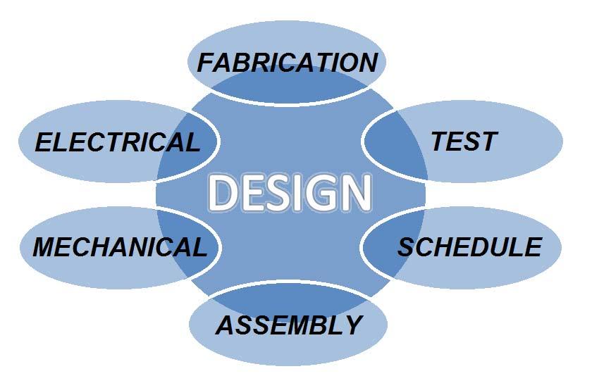
3 Every manufacturer I ve ever known, are always encouraging us to be forward thinkers. We can best do this by being prepared, planning ahead, to research and anticipate! ***Therefore as designers we Collaborate*** Definition of Collaborate: to work with another person or group in order to achieve or do something Our goal as designers is not to just design a board, but rather it s to design a board so that it can be built well!
4 Are your designs Correct by construction? How many boards do you manufacture? #### unless you re a manufacturer, the answer is Qualify your vendor: visit, learn their process, learn their capabilities, speak their language, build a relationship, know the person Do you know the build plan proto to prod.? Do you proto-type where you build production runs? PROs and CONs Will purchasing select the vendor and if so when? PROs and CONs
5 Producibility Levels [IPC-2221A 1.6.3] established to help communicate the design complexity to the manufacturers DESIGNER FABRICATOR ASSEMBLER Producibility levels are NOT design requirements Ask the question, Is it technologically appropriate for this vendor?
6 tooling materials processing Producibility Levels reflect progressive increases in the sophistication of: YIELDS COSTS Hence, progressive increases in fabrication cost$
7
8 Design for Excellence (DFX) DFM - Design for Manufacturing (Fabrication) DFA - Design for Assembly DFT - Design for Test DFR Design for Reliability DFE Design for the Environment


9 Making contact should not be optional; it should be standard operating procedure
10 When do you communicate to your manufacturing chain? Is it in the 11 th hour or is it proactively? When can I get a quote from my fabricator? When are the feature sizes confirmed? How and when do you validate your design? When is the best time for a DFM review? What is required: Complete or partial data; How about a PO? Collaboration should start at the initial estimation of a design!

11 * 18 layers 1.6mm Thk., 10 Ghz, DDR4, 1760 BGA 300 hours, 2 Months How would you like to get to this point and then find out it s unbuildable?
12 Type of end use for a board Build plan High volume production Or is it development or debug Class 2 or Class 3 Number of I/O signals on a BGA can determine the layer count HDI methods allowed Feasibility Dispersement Study Type of circuitry High-Speed or RF Schedule requirements
13 As speed and performance increased, so did the heat We all know that heat is not our friend So voltages had to come down As voltage drop, so the size & pitch were reduced As performance went up so did the pin count go up Result equaled Smaller case size Increased pin count Lower voltage Increased thermal And did I mention it must cost less and be done faster!
14 Placement Feasibility SMT Parts will not fit with room for pin escapes to PTH vias Standard PTH vias are too large to pin-escape a ubga (Typically a.65mm or below pitch device) High Speed or RF performance unwanted parasitics or excess inductance from standard PTH vias Increased routing density from high pin count devices. Limited layer count per 1.6mmThk. Bd. Back to back large active SMT devices BGA s RF on Primary Side / Digital on Secondary side
15 Package type Common Land Pitches in Package Family No. Pins Description SOIC/FQFP Small outline IC Peripheral Peripheral or grid array QFP/PGA/BGA Quad flat pack/pin grid array/ball grid array Peripheral and grid array BGA/QFP Pitch size 0.5, 0.4, 0.3mm & PGA Grid array BGA > 2000 Large scale integration Grid array BGA s ball grid arrays were standardized in the 1990's The pin pitch was 1.5 mm [0.060 in], and 1.27 mm [0.050 in] As smaller and smaller parts evolved they include pitches of 1.0 mm, 0.8, 0.65, 0.5, 0.4, 0.3, and 0.25 mm. (80% rule)


16 100 Pin 1.0mm 100 Pin.80mm 100 Pin.65mm 100 Pin.50mm 100 Pin.40mm 2116 Pin 1.0mm 90 Pin.80mm DDR


17 Common Discrete SMT Case Common Active SMT Case Images courtesy of PCB Libraries, Inc.

18 Usable Placement Area Primary & Secondary Sides Usable Board Placement Area

19 Primary Side: Active Devices Shown in Blue Secondary Side: Passive Devices Shown in Red Usable Placement Area Primary & Secondary Sides Quick component dispersement shows some feasibility, thus DFM/DFA ready
20 Data: Preliminary and/or Final Feature sizes Materials Capabilities and process adjustments Build plan and schedule Process steps vs. turn-time
21 Symbol Feature Conventional m [inch] Threshold m [inch] Leading edge m [inch] State-of-the-art m [inch] a minimum micro-via size on target land 100 [0.004] 75 [0.003] 75 [0.003] 50 [0.002] b maximum micro-via size on capture land 110 [0.004] 80 [0.003] 80 [0.003] 60 [0.002] c target land size 350 [0.014] 300 [0.012] 250 [0.010] 130 [0.005] d capture land size 350 [0.014] 300 [0.012] 250 [0.010] 130 [0.005] e minimum conductor on RDL 125 [0.005] 100 [0.004] 75 [0.003] 50 [0.002] f minimum conductor space on RDL 125 [0.005] 100 [0.004] 75 [0.010] 50 [0.002] g minimum land with maximum PTH for that land 800 [0.031] 600 [0.024] 400 [0.016] 250 [0.010] h minimum PTH diameter 350 [0.014] 250 [0.010] 125 [0.005] 100 [0.004] i minimum pitch between micro-vias 1250 [.0049] 800 [0.031] 500 [0.020] 250 [0.010] j minimum dielectric thickness RDL 60 [0.002] 50 [0.002] 50 [0.002] 25 [0.001] k minimum plating thickness in core vias 25 [0.001] 20 [0.001] 17 [0.001] 17 [0.001] l minimum plating thickness in PTH 25 [0.001] 20 [0.001] 17 [0.001] 17 [0.001] m minimum plating thickness in micro-via 25 [0.001] 20 [0.001] 17 [0.001] 17 [0.001] n minimum board thickness not including plating 800 [0.031] 700 [0.028] 600 [0.024] 600 [0.024] Important Ratios a/j Maximum aspect ratio for micro-via All copper thicknesses are 17 m Plating thickness for 2 to n-1 layer to be nominal 17 m, minimum 12.5 m Annular ring (AR) is land allowance per side of hole. Land diameter equals finished hole size (FHS) + 2x AR. Maximum board thickness requires trade-offs. Contact your supplier
22


23 What happens to the quick turn schedule if desired material is not in stock? unexpected delays
24 Customer Data Sales Engineering Review Design for Manufacturability CAM Laser Data / Plot Film Issue Material Dry Film Prep & Coat Inner Layers LDI / Photo Image Inner Layers DES (Develop, Etch, Strip) AOI Inner Layers Oxide Treatment Lamination CNC Drill Hole Debur UV Laser Ablation Hole Desmear Electroless Copper Dry Film Prep & Coat Outer Layers LDI / Photo Image Outer Layers Develop Pattern Plate Copper Tin Plate (Etch Resist) Strip & Etch AOI Outer Layers Soldermask Alt. Finishes HASL / ENIG / Immersion Tin Electrolytic Au Plate (Optional) Legend Soldermask Via Plug Fabrication Electrical Test TDR Test (Optional) Final Inspectio n Final Clean OSP Coating or Immersion Silver (Optional) Ship Custome r


25 Note the 2x - Nx for build-up of multi-lamination cycles- Top right image 4 laminations Process steps can take time!
26 Stack-up and impedance: Who's formula or calculator do you use? Answer: Whatever you do, consider it a starting point and submit it to the fabricator early. What material is in stock? What are the process adjustments they will use? Are the feature sizes and process adjustments good for multiple vendors?

27 Stack-up Request: submitted very early in design phase
28 Designed CLASS 3 or 3A Is it buildable? The answer to this question can be subjective. The answer is a collaborative result of feature sizes as they relate to manufacturing allowances and process requirements per IPC 2221 and IPC Class 3 or Class 3A design (Appendix A, what revision?) (1mil or 2mil Internal Annular Ring) Does the fabricator agree based on our design features, aspect ratio and plating requirements?
29 What s a panel? Does your Assembly Array provide a good Fabrication Panel utilization or yield? Fab and Assy may be different vendors and have different goals. Collaboration is the key! What are the tolerances in your CAD design data? Answer: None. It s actually True Position data What are the tolerances in your manufactures process? Answer: Many. What is the difference? Mfg. Process Allowances How are these documented? How many designers don t understand their own fabrication notes?


30 A Responsible PCB Designer or Engineer should understand these notes as they relate to their board

31 Chart / Data Courtesy PWB Interconnect


32 Stacked Vias


33 Stacking of laser vias: Tests have shown that multiple stacked laser vias are stable due to the thinner dielectrics and the plated fill. However, it is not recommended to stack laser vias on top of mechanical buried vias; due to the epoxy fill which creates dissimilar Z-Axis CTE issues.


34 IST Tester Interconnect Stress HATSTM Tester Highly Accelerated Thermal Shock Best way to have good test results is to design for high yield manufacturing via collaboration.

35 We want a board that would function and perform well. We also want to have a high manufacturing yield to our build, thus lowering cost. Collaborating with your manufacturing team through the entire layout phase is the best way to design a correct by construction circuit. The best solution to any problem is to preclude it!

36 Remember IPC is not a THEM, it s an US! Thank you, very much! Michael R. Creeden CEO/CID+ San Diego PCB, Inc. mike.creeden@sdpcb.com (858)
AltiumLive 2017: Creating Documentation for Successful PCB Manufacturing
 AltiumLive 2017: Creating Documentation for Successful PCB Manufacturing Julie Ellis TTM Field Applications Engineer Thomas Schneider Field Applications Engineer 1 Agenda 1 Complexity & Cost 2 3 4 5 6
PCB Fabrication Processes Brief Introduction
 PCB Fabrication Processes Brief Introduction AGS-Electronics, Ph: +1-505-550-6501 or +1-505-565-5102, Fx: +1-505-814-5778, Em: sales@ags-electronics.com, Web: http://www.ags-electronics.com Contents PCB
Low-Cost PCB Design 1
 Low-Cost PCB Design 1 PCB design parameters Defining PCB design parameters begins with understanding: End product features, uses, environment, and lifetime goals PCB performance, manufacturing, and yield
Overcoming the Challenges of HDI Design
 ALTIUMLIVE 2018: Overcoming the Challenges of HDI Design Susy Webb Design Science Sr PCB Designer San Diego Oct, 2018 1 Challenges HDI Challenges Building the uvia structures The cost of HDI (types) boards
METRIC PITCH BGA AND MICRO BGA ROUTING SOLUTIONS
 White Paper METRIC PITCH BGA AND MICRO BGA ROUTING SOLUTIONS June 2010 ABSTRACT The following paper provides Via Fanout and Trace Routing solutions for various metric pitch Ball Grid Array Packages. Note:
South Bay Circuits. Manufacturability Guidelines. Printed Circuit Boards FOR. South Bay Circuits, Inc. 99 N. McKemy Ave Chandler, AZ 85226
 Manufacturability Guidelines FOR Printed Circuit Boards South Bay Circuits, Inc. 99 N. McKemy Ave Chandler, AZ 85226 GL-0503B By: Edward Rocha Dear Customer, The intention of this document is to provide
Generic Multilayer Specifications for Rigid PCB s
 Generic Multilayer Specifications for Rigid PCB s 1.1 GENERAL 1.1.1 This specification has been developed for the fabrication of rigid SMT and Mixed Technology Multilayer Printed Circuit Boards (PCB's)
Application Note 5026
 Surface Laminar Circuit (SLC) Ball Grid Array (BGA) Eutectic Surface Mount Assembly Application Note 5026 Introduction This document outlines the design and assembly guidelines for surface laminar circuitry
TOLERANCE FORGOTTEN: IMPACTS OF TODAY S COMPONENT PACKAGING AND COPPER ROUTING ON ELECTRONIC
 TOLERANCE FORGOTTEN: IMPACTS OF TODAY S COMPONENT PACKAGING AND COPPER ROUTING ON ELECTRONIC Presented By: Dale Lee E-mail: Dale.Lee@Plexus.Com April 2013 High Layer Counts Wide Range Of Component Package
DESIGN FOR MANUFACTURABILITY (DFM)
") T H A N K S F O R A T T E N D I N G OUR TECHNICAL WEBINAR SERIES DESIGN FOR MANUFACTURABILITY (DFM) Presented by: We don t just sell PCBs. We sell sleep. Cirtech EDA is the exclusive SA representative
T H A N K S F O R A T T E N D I N G OUR TECHNICAL WEBINAR SERIES DESIGN FOR MANUFACTURABILITY (DFM) Presented by: We don t just sell PCBs. We sell sleep. Cirtech EDA is the exclusive SA representative
CAPABILITIES OF SYNERGISE PCB INC
 CAPABILITIES OF SYNERGISE PCB INC 2 Surface Treatment Surface Treatment Selective Surface Treatment HASL, L/F HASL, ENIG, Immersion Silver, Hard Gold(Plated gold), Flash Gold, Immersion Tin/Silver, OSP
What the Designer needs to know
 White Paper on soldering QFN packages to electronic assemblies. Brian J. Leach VP of Sales and Marketing AccuSpec Electronics, LLC Defect free QFN Assembly What the Designer needs to know QFN Description:
CAPABILITIES Specifications Vary By Manufacturing Locations
 Revised June 2011 Toll Free: 1-800-979-4PCB (4722) www.4pcb.com sales@4pcb.com Material FR4 RoHS RF Materials CAPABILITIES Specifications Vary By Manufacturing Locations Number of Conductive Layers Standard
High Performance Package Trends Driving BackDrill File Generation Using Cadence Allegro. Chris Heard and Leigh Eichel
 High Performance Package Trends Driving BackDrill File Generation Using Cadence Allegro By Chris Heard and Leigh Eichel 1. Introduction As the semiconductor industry passes the 100 billion unit mark for
Sectional Design Standard for High Density Interconnect (HDI) Printed Boards
 Printed Boards") IPC-2226 ASSOCIATION CONNECTING ELECTRONICS INDUSTRIES Sectional Design Standard for High Density Interconnect (HDI) Printed Boards Developed by the HDI Design Subcommittee (D-41) of the HDI Committee
IPC-2226 ASSOCIATION CONNECTING ELECTRONICS INDUSTRIES Sectional Design Standard for High Density Interconnect (HDI) Printed Boards Developed by the HDI Design Subcommittee (D-41) of the HDI Committee
Sunstone Circuits DFMplus Summary Report
 Job Name DFM081-wireless_controller_v0 Part Number Wireless_Controller Customer Name Contact Name Job Class IPC Class 2 Job View Creation Time 2014-08-14 15:55:31 Revision V0 Operator Name lyndap Contact
FPGA World Conference Stockholm 08 September John Steinar Johnsen -Josse- Senior Technical Advisor
 FPGA World Conference Stockholm 08 September 2015 John Steinar Johnsen -Josse- Senior Technical Advisor Agenda FPGA World Conference Stockholm 08 September 2015 - IPC 4101C Materials - Routing out from
PCB technologies and manufacturing General Presentation
 PCB technologies and manufacturing General Presentation 1 Date : December 2014 3 plants for a global offer dedicated to the European market and export Special technologies, Harsh environment PCB for space
TCLAD: TOOLS FOR AN OPTIMAL DESIGN
 TCLAD: TOOLS FOR AN OPTIMAL DESIGN THINGS TO CONSIDER WHEN DESIGNING CIRCUITS Many factors come into play in circuit design with respect to etching, surface finishing and mechanical fabrication processes;
Design For Manufacture
 NCAB Group Seminar no. 11 Design For Manufacture NCAB GROUP Design For Manufacture Design for manufacture (DFM) What areas does DFM give consideration to? Common errors in the documentation Good design
Sectional Design Standard for Flexible/Rigid-Flexible Printed Boards
 Sectional Design Standard for Flexible/Rigid-Flexible Printed Boards Developed by the Flexible Circuits Design Subcommittee (D-) of the Flexible Circuits Committee (D-0) of IPC Supersedes: IPC-2223C -
Technical Capabilities Non Standard Technologies. CML pcbs from just around the corner
 Technical Capabilities Non Standard Technologies PAGE 1 Capabilities Rigid Layer Count 1-12 layer (above 12 layer see HDI) 0.4-3.2 mm (> 3.2 mm on request) Finished Board Thickness Tolerance: +/-10% Core
Laminate Based Fan-Out Embedded Die Technologies: The Other Option
 Laminate Based Fan-Out Embedded Die Technologies: The Other Option Theodore (Ted) G. Tessier, Tanja Karila*, Tuomas Waris*, Mark Dhaenens and David Clark FlipChip International, LLC 3701 E University Drive
Artwork: (A/W) An accurately scaled configuration used to produce the artwork master or production master.
 An accurately scaled configuration used to produce the artwork master or production master.") Adhesive: The material used for bonding two substrates of material together. (usually; LF of FR 0100) Adhesive Squeeze-Out: Adhesive will ooze out slightly during the lamination cycle. Annular Ring: That
Adhesive: The material used for bonding two substrates of material together. (usually; LF of FR 0100) Adhesive Squeeze-Out: Adhesive will ooze out slightly during the lamination cycle. Annular Ring: That
NextGIn( Connec&on'to'the'Next'Level' Application note // DRAFT Fan-out 0,50mm stapitch BGA using VeCS. Joan Tourné NextGIn Technology BV
 NextGIn( Connec&on'to'the'Next'Level' Application note // DRAFT Fan-out 0,50mm stapitch BGA using VeCS. Joan Tourné NextGIn Technology BV February 27 th 2017 In this document we describe the use of VeCS
The Effects of PCB Fabrication on High-Frequency Electrical Performance
 As originally published in the IPC APEX EXPO Conference Proceedings. The Effects of PCB Fabrication on High-Frequency Electrical Performance John Coonrod, Rogers Corporation Advanced Circuit Materials
Technology Overview. Blind Micro-vias. Embedded Resistors. Chip-on-flex. Multi-Tier Boards. RF Product. Multi-chip Modules. Embedded Capacitance
 Blind Micro-vias Embedded Resistors Multi-Tier Boards Chip-on-flex RF Product Multi-chip Modules Embedded Capacitance Technology Overview Fine-line Technology Agenda Corporate Overview Company Profile
!"#$"%&' ()#*+,-+.&/0(
#*+,-+.&/0(") !"#$"%&' ()#*+,-+.&/0( Multi Chip Modules (MCM) or Multi chip packaging Industry s first MCM from IBM. Generally MCMs are horizontal or two-dimensional modules. Defined as a single unit containing two
!"#$"%&' ()#*+,-+.&/0( Multi Chip Modules (MCM) or Multi chip packaging Industry s first MCM from IBM. Generally MCMs are horizontal or two-dimensional modules. Defined as a single unit containing two
Optimalisation of the PCB design and PCB production to control cost
 Optimalisation of the PCB design and PCB production to control cost Edward Snelleman 1 Introduction Q.P.I. Group 1988 started to be active in the field of PCB supply/development and PCB Design 2015 member
ATTRIBUTES STANDARD ADVANCED
 TECHNOLOGY MATRIX 2017 ATTRIBUTES STANDARD ADVANCED Line/Space.005 /.005.003 /.003 Copper Foil. Oz. Min/Max ½ / 2 3 / 8 Pad Size Int. (dia over Drill).014.008 Pad Size Ext. (dia over Drill).012.008 Drill-to-Metal
Technology Flexible Printed Circuits Rev For latest information please visit
 Options and Characteristics Online calculation On explicit enquiry Quantity 1 pieces up to 1m² total area 1piece to mass production Number of layers 1 to 2 layers up to 6 layers Material thickness 0,05mm
Advanced High-Density Interconnection Technology
 Advanced High-Density Interconnection Technology Osamu Nakao 1 This report introduces Fujikura s all-polyimide IVH (interstitial Via Hole)-multi-layer circuit boards and device-embedding technology. Employing
The Effects of PCB Fabrication on High-Frequency Electrical Performance
 The Effects of PCB Fabrication on High-Frequency Electrical Performance John Coonrod, Rogers Corporation Advanced Circuit Materials Division Achieving optimum high-frequency printed-circuit-board (PCB)
Flip-Chip PBGA Package ConstructionÑ Assembly and Board-Level Reliability
 Order Number: AN1850/D Rev. 0, 5/2000 Application Note Flip-Chip PBGA Package ConstructionÑ Assembly and Motorola introduced the ßip-chip plastic ball grid array (FC PBGA) packages as an alternative to,
Design for Manufacturability of Rigid Multi-Layer Boards By: Tom Hausherr
 Design for Manufacturability of Rigid Multi-Layer Boards By: Tom Hausherr INTRODUCTION SECTION CONTENTS PAGE 1 INTRODUCTION...1-3 2 RAW MATERIALS SELECTION...2-3 2.1 Material Selection and Panel Utilization...2-3
Manufacture and Performance of a Z-interconnect HDI Circuit Card Abstract Introduction
 Manufacture and Performance of a Z-interconnect HDI Circuit Card Michael Rowlands, Rabindra Das, John Lauffer, Voya Markovich EI (Endicott Interconnect Technologies) 1093 Clark Street, Endicott, NY 13760
Practical Guidelines for the Implementation of Back Drilling Plated Through Hole Vias in Multi-gigabit Board Applications DesignCon 2003
 DesignCon 2003 Abstract Title: Practical Guidelines for the implementation of back drilling plated through hole vias in multi-gigabit board applications Author: Tom Cohen Tom Cohen Tom is currently a principle
Electrical Testing of Passive Components
 feature Electrical Testing of Passive Components by Todd L. Kolmodin, Manfred Ludwig, Howard Carpenter and Rick Meraw Gardien Services USA and China Introduction Substrates have become more critical with
Ace Tech Circuit Presentation
 Presentation (ZIP)429-912 1254-8, Jeongwang-Dong, Siheung-si, GyeongGi-Do, Korea (New Address : 32 (#509-1Na Dong), 79 Beon-Gil, Gong Dan 1 Daero, (Jeong Wang Dong ShiWha Industrial CPLX ) Shi-Heung City,
Improve SMT Assembly Yields Using Root Cause Analysis in Stencil Design
 Improve SMT Assembly Yields Using Root Cause Analysis in Stencil Design Greg Smith FCT Assembly, Inc. gsmith@fctassembly.com This paper and presentation was first presented at the 2017 IPC Apex Expo Technical
Improve SMT Assembly Yields Using Root Cause Analysis in Stencil Design
 Improve SMT Assembly Yields Using Root Cause Analysis in Stencil Design Greg Smith FCT Assembly, Inc. gsmith@fctassembly.com This paper and presentation was first presented at the 2017 IPC Apex Expo Technical
Probe. Placement P Primer P. Copyright 2011, Circuit Check, Inc.
 Probe Placement P Primer P What's Involved? Control Design ICT Friendly UUT Location Location Location Increase your odds in the manufacturing process Good contact Small targets Agilent Bead Probes Suggested
PCB Manufacture Capabilities
 Item Unit Description or parameter 1 Arlon material model AD350,AR1000,25FR,33N,Diclad527 2 Rogers material model Ro4350,Ro4350B,Ro4003,Ro4003C,Ro3003,RT5880 3 Rogers PP model Ro4403(0.10mm),Ro4450B(0.10mm),
BGA (Ball Grid Array)
") BGA (Ball Grid Array) National Semiconductor Application Note 1126 November 2002 Table of Contents Introduction... 2 Package Overview... 3 PBGA (PLASTIC BGA) CONSTRUCTION... 3 TE-PBGA (THERMALLY ENHANCED
BGA (Ball Grid Array) National Semiconductor Application Note 1126 November 2002 Table of Contents Introduction... 2 Package Overview... 3 PBGA (PLASTIC BGA) CONSTRUCTION... 3 TE-PBGA (THERMALLY ENHANCED
Features. Preliminary. = +25 C, IF = 1 GHz, LO = +13 dbm*
 Typical Applications Features The is ideal for: Test Equipment & Sensors Point-to-Point Radios Point-to-Multi-Point Radios Military & Space Functional Diagram Wide IF Bandwidth: DC - 17 GHz Input IP3:
STENCIL CONSIDERATIONS FOR MINIATURE COMPONENTS
 STENCIL CONSIDERATIONS FOR MINIATURE COMPONENTS William E. Coleman, Ph.D. Photo Stencil Colorado Springs, CO, USA ABSTRACT SMT Assembly is going through a challenging phase with the introduction of miniature
APPLICATION NOTE 6381 ORGANIC LAND GRID ARRAY (OLGA) AND ITS APPLICATIONS
 AND ITS APPLICATIONS") Keywords: OLGA, SMT, PCB design APPLICATION NOTE 6381 ORGANIC LAND GRID ARRAY (OLGA) AND ITS APPLICATIONS Abstract: This application note discusses Maxim Integrated s OLGA and provides the PCB design and
Keywords: OLGA, SMT, PCB design APPLICATION NOTE 6381 ORGANIC LAND GRID ARRAY (OLGA) AND ITS APPLICATIONS Abstract: This application note discusses Maxim Integrated s OLGA and provides the PCB design and
Product Specification - LPM Connector Family
 LPM Product Specification - LPM OVERVIEW Developed for mobile devices and other space-constrained applications, the Neoconix LPM line of connectors feature exceptional X-Y-Z density with a simple, highly
Interposer MATED HEIGHT
 Product Specification: FEATURES High Performance PCBeam Connector Technology Product options at 1.27mm, 1.0mm, and 0.8mm pitch Maximized pin count per form factor 3 form factor sizes available Standard
Broadband Printing: The New SMT Challenge
 Broadband Printing: The New SMT Challenge Rita Mohanty & Vatsal Shah, Speedline Technologies, Franklin, MA Gary Nicholls, Ron Tripp, Cookson Electronic Assembly Materials Engineered Products, Johnson City,
Bob Willis Process Guides
 What is a Printed Circuit Board Pad? What is a printed circuit board pad, it may sound like a dumb question but do you stop to think what it really does and how its size is defined and why? A printed circuit
PCB Trace Impedance: Impact of Localized PCB Copper Density
 PCB Trace Impedance: Impact of Localized PCB Copper Density Gary A. Brist, Jeff Krieger, Dan Willis Intel Corp Hillsboro, OR Abstract Trace impedances are specified and controlled on PCBs as their nominal
Processing parameters of PCBs manufactured by TS PCB Techno-Service S.A.
 Processing parameters of PCBs manufactured by TS PCB Techno-Service S.A. Last update: jh 26.09.2017 Table of contents 1. Processing parameters of PCB materials... 3 1.1. Applied laminate types... 3 1.2.
Vol. 58 No. 7. July MVP NI AWR Design Environment. Founded in 1958
 Vol. 58 No. 7 July 215.com MVP NI AWR Design Environment Founded in 1958 98 MICROWAVE JOURNAL JULY 215 Managing Circuit Materials at mmwave Frequencies John Coonrod Rogers Corp., Chandler, Ariz. This article
Printed circuit boards-solder mask design basics
 Printed circuit boards-solder mask design basics Standards Information on the use of solder mask is contained in IPC-SM-840C Qualification and Performance of Permanent Solder Mask. The specification is
CIA GENERAL SPECIFICATION. For Double-sided and Multi-layer Printed Circuit Boards. Version 1.4
 CIA GENERAL SPECIFICATION For Double-sided and Multi-layer Printed Circuit Boards Version 1.4 Records of Revision Date Paragraph Page Summary Latest Version 04-10-24 First Issue 1.0 14-06-09 ccl 1.2 10-07-14
Enabling Parallel Testing at Sort for High Power Products
 Enabling Parallel Testing at Sort for High Power Products Abdel Abdelrahman Tim Swettlen 2200 Mission College Blvd. M/S SC2-07 Santa Clara, CA 94536 Abdel.Abdelrahman@intel.com Tim.Swettlen@intel.com Agenda
U.S. Circuit, Inc. Design for Manufacturability Guide
 U.S. Circuit, Inc. Design for Manufacturability Guide U S Circuit, Inc. Page 1 02/10/2016 TABLE OF CONTENTS Introduction Panels Materials Guidelines Step & Repeat Coupons IPC-4101 Base Materials Slash-Sheet
Multilayer PCB Stackup Planning
 by Barry Olney In-Circuit Design Pty Ltd Australia This Application Note details tried and proven techniques for planning high speed Multilayer PCB Stackup configurations. Planning the multilayer PCB stackup
Innovations Push Package-on-Package Into New Markets. Flynn Carson. STATS ChipPAC Inc Kato Rd Fremont, CA 94538
 Innovations Push Package-on-Package Into New Markets by Flynn Carson STATS ChipPAC Inc. 47400 Kato Rd Fremont, CA 94538 Copyright 2010. Reprinted from Semiconductor International, April 2010. By choosing
EMERGING SUBSTRATE TECHNOLOGIES FOR PACKAGING
 EMERGING SUBSTRATE TECHNOLOGIES FOR PACKAGING Henry H. Utsunomiya Interconnection Technologies, Inc. Suwa City, Nagano Prefecture, Japan henryutsunomiya@mac.com ABSTRACT This presentation will outline
PCB Routing Guidelines for Signal Integrity and Power Integrity
 PCB Routing Guidelines for Signal Integrity and Power Integrity Presentation by Chris Heard Orange County chapter meeting November 18, 2015 1 Agenda Insertion Loss 101 PCB Design Guidelines For SI Simulation
mcube LGA Package Application Note
 AN-001 Rev.02 mcube LGA Package Application Note AN-001 Rev.02 mcube, Inc. 1 / 21 AN-001 Rev.02 Guidelines for Printed Circuit Board (PCB) Design and Assembly with mcube Land Grid Array (LGA) Package Sensors
PCB Design considerations
 PCB Design considerations Better product Easier to produce Reducing cost Overall quality improvement PCB design considerations PCB Design to assure optimal assembly Place at least 3 fiducials (global fiducial)
Embedded Thin Film Resistors
 Embedded Thin Film Resistors An Update on Current Applications & Design Bruce Mahler Vice President Ohmega Technologies, Inc. IPC Designers Council Orange County Chapter July 19, 2017 NiP Thin Film Resistive
Silicon Interposers enable high performance capacitors
 Interposers between ICs and package substrates that contain thin film capacitors have been used previously in order to improve circuit performance. However, with the interconnect inductance due to wire
Downloaded from MSFC-STD-3425 National Aeronautics and. BASELINE Space Administration December 12, 2006 EI42
 MSFC-STD-3425 National Aeronautics and BASELINE Space Administration December 12, 2006 George C. Marshall Space Flight Center Marshall Space Flight Center, Alabama 35812 EI42 MULTIPROGRAM/PROJECT COMMON-USE
Value Stream Map Process Flow
 Value Stream Map Process Flow Pre- Locate Data Value Stream Mapping Has The Following Characteristics: It Is A Comprehensive And Detailed Graphical Document That Lists Every Business Unit, Organization,
Design For Manufacturability
 Colonial ELECTRONIC MANUFACTURERS, INCORPORATED Design For Manufacturability GUIDELINES DFM-1 REV-C One Chestnut Street Nashua, New Hampshire 03060 Telephone: (603) 881-8244 FAX: (603) 881-8186 1 DFM-1
AltiumLive 2017: 8 NEW DESIGN FEATURES OF HIGH DENSITY PWBS
 AltiumLive 2017: 8 NEW DESIGN FEATURES OF HIGH DENSITY PWBS Happy Holden PCB Technologist San Diego, October 4 th 2017 Agenda What HDI Design Features Gain The Most 1 Where to place the blind vias 2 3
Features. = +25 C, Vdd = 5V, Idd = 85 ma*
 Typical Applications The is an ideal gain block or driver amplifi er for: Point-to-Point Radios Point-to-Multi-Point Radios VSAT Functional Diagram Features Saturated Power: +23 dbm @ 27% PAE Gain: db
BLIND MICROVIA TECHNOLOGY BY LASER
 BLIND MICROVIA TECHNOLOGY BY LASER Larry W. Burgess LaserVia Drilling Centers, L.L.C. Wilsonville, Oregon, USA ABSTRACT The most costly process in the fabrication of today's multilayer printed circuit
mcube WLCSP Application Note
 AN-002 Rev.02 mcube WLCSP Application Note AN-002 Rev.02 mcube, Inc. 1 / 20 AN-002 Rev.02 Guidelines for Printed Circuit Board (PCB) Design and Assembly with mcube Wafer Level Chip Scale Package (WLCSP)
Product Specification - LPS Connector Series
 LPS Product Specification - LPS OVERVIEW The LPS products are solderable versions of those in the Neoconix LPM product series. Also developed for mobile devices and other space-constrained applications,
Improving Density in Microwave Multilayer Printed Circuit Boards for Space Applications
 Improving Density in Microwave Multilayer Printed Circuit Boards for Space Applications David NÉVO (1) Olivier VENDIER (1), Jean-Louis CAZAUX (1), Jean-Luc LORTAL (2) (1) Thales Alenia Space 26 avenue
CIA GENERAL SPECIFICATION. For Double-sided and Multi-layer Printed Circuit Boards. Version 1.3
 CIA GENERAL SPECIFICATION For Double-sided and Multi-layer Printed Circuit Boards Version 1.3 Records of Revision Date Paragraph Page Summary Latest Version 04-10-24 First Issue 1.0 09-06-14 ccl 1.2 14-07-10
An Introduction to Electronics Systems Packaging. Prof. G. V. Mahesh. Department of Electronic Systems Engineering
 An Introduction to Electronics Systems Packaging Prof. G. V. Mahesh Department of Electronic Systems Engineering India Institute of Science, Bangalore Module No. # 02 Lecture No. # 08 Wafer Packaging Packaging
HOW DOES SURFACE FINISH AFFECT SOLDER PASTE PERFORMANCE?
 HOW DOES SURFACE FINISH AFFECT SOLDER PASTE PERFORMANCE? Tony Lentz FCT Assembly Greeley, CO, USA tlentz@fctassembly.com ABSTRACT The surface finishes commonly used on printed circuit boards (PCBs) have
Webinar: Suppressing BGAs and/or multiple DC rails Keith Armstrong. 1of 5
 1of 5 Suppressing ICs with BGA packages and multiple DC rails Some Intel Core i5 BGA packages CEng, EurIng, FIET, Senior MIEEE, ACGI Presenter Contact Info email: keith.armstrong@cherryclough.com website:
14.8 Designing Boards For BGAs
 exposure. Maintaining proper control of moisture uptake in components is critical to the prevention of "popcorning" of the package body or encapsulation material. BGA components, before shipping, are baked
PAST, PRESENT AND FUTURE OF SOLDERLESS ASSEMBLY
 PAST, PRESENT AND FUTURE OF SOLDERLESS ASSEMBLY Joseph Fjelstad Verdant Electronics Sunnyvale, CA, USA joe@verdantelectronics.com ABSTRACT The forced transition to lead-free soldering foisted on the global
Application Bulletin 240
 Application Bulletin 240 Design Consideration CUSTOM CAPABILITIES Standard PC board fabrication flexibility allows for various component orientations, mounting features, and interconnect schemes. The starting
Design Guide for High-Speed Controlled Impedance Circuit Boards
 IPC-2141A ASSOCIATION CONNECTING ELECTRONICS INDUSTRIES Design Guide for High-Speed Controlled Impedance Circuit Boards Developed by the IPC Controlled Impedance Task Group (D-21c) of the High Speed/High
PCB workshop at ESTEC in Noordwijk
 PROPRIETARY INFORMATION reserves all rights including in Noordwijk ESA MIL IPC Page 1 PROPRIETARY INFORMATION reserves all rights including Introduction Thomas Maihöfer Dipl.- Ing (FH) 1970 1991 1995 1995
Innovative pcb solutions used in medical and other devices Made in Switzerland
 Innovative pcb solutions used in medical and other devices Made in Switzerland Chocolate Watches Money.PCB`s innovative pcb`s... Customer = innovation driver Need to add more parts and I/O make smaller/thinner
WIRE LAYING METHODS AS AN ALTERNATIVE TO MULTILAYER PCB Sf
 Electrocomponent Science and Technology, 1984, Vol. 11, pp. 117-122 (C) 1984 Gordon and Breach Science Publishers, Inc 0305-3091/84/1102-0117 $18.50/0 Printed in Great Britain WIRE LAYING METHODS AS AN
Improve SMT Assembly Yields Using Root Cause Analysis in Stencil Design
 Improve SMT Assembly Yields Using Root Cause Analysis in Stencil Design Greg Smith FCT Assembly, Inc. Greeley, CO Abstract Reduction of first pass defects in the SMT assembly process minimizes cost, assembly
High currents in safe paths
 High currents in safe paths Webinar November 3 rd 2015 Speaker: Andreas Schilpp www.we-online.de topics Flex-rigid technology with thick copper layers Update Design Rules Wirelaid Update UL-Listing Wirelaid
Design for Manufacturing
 2 Design for Manufacturing This chapter will address the fabrication process of the PCB and the requirements of the manufacturer. Manufacturers are separated by their limitations or constraints into categories
Features. = +25 C, As a Function of LO Drive & Vdd. IF = 1 GHz LO = -4 dbm & Vdd = +4V
 v1.121 SMT MIXER, 2-3 GHz Typical Applications The is ideal for: 2 and 3 GHz Microwave Radios Up and Down Converter for Point-to-Point Radios LMDS and SATCOM Features Integrated LO Amplifi er: Input Sub-Harmonically
High Frequency Single & Multi-chip Modules based on LCP Substrates
 High Frequency Single & Multi-chip Modules based on Substrates Overview Labtech Microwave has produced modules for MMIC s (microwave monolithic integrated circuits) based on (liquid crystal polymer) substrates
Hardware Design Considerations for MKW41Z/31Z/21Z BLE and IEEE Device
 NXP Semiconductors Document Number: AN5377 Application Note Rev. 2, Hardware Design Considerations for MKW41Z/31Z/21Z BLE and IEEE 802.15.4 Device 1. Introduction This application note describes Printed
Creating another Printed Circuit Board
 Appendix C Creating another Printed Circuit Board In this chapter, we will learn the following to World Class standards: Starting with a Finished Schematic Creating the Layers for the Printed Circuit Board
Page 1
 CONTENT INTRODUCTION 2 INPUT DATA FORMATS 3 INPUT DATA REQUIREMENTS 4 CLASSIFICATION 6 HOLES 8 COPPER LAYERS 10 BGAS 12 MECHANICAL LAYER 13 SOLDERMASK 15 LEGEND PRINT 17 CARBON 18 PEEL-OFF MASK 19 VIAFILL
Ruth Kastner Eli Moshe. Embedded Passives, Go for it!
 Ruth Kastner Eli Moshe Embedded Passives, Go for it! Outline Description of a case study: Problem definition New technology to the rescue: Embedded passive components Benefits from new technology Design
MICROELECTRONICS ASSSEMBLY TECHNOLOGIES. The QFN Platform as a Chip Packaging Foundation
 West Coast Luncheon January 15, 2014. PROMEX PROMEX INDUSTRIES INC. MICROELECTRONICS ASSSEMBLY TECHNOLOGIES The QFN Platform as a Chip Packaging Foundation 3075 Oakmead Village Drive Santa Clara CA Ɩ 95051
High Efficient Heat Dissipation on Printed Circuit Boards. Markus Wille, R&D Manager, Schoeller Electronics Systems GmbH
 High Efficient Heat Dissipation on Printed Circuit Boards Markus Wille, R&D Manager, Schoeller Electronics Systems GmbH m.wille@se-pcb.de Introduction 2 Heat Flux: Q x y Q z The substrate (insulation)
10. Mini Coax Connectors
 . Connectors The allows multi-pole coaxial data transmission for board-to-board, cable-to-board and cable-to-cable applications with protection up to IP 65 / IP 67. At the same time, applications up to
IEEE Joint Section Reliability Chapter. Dramatic COTs Pro Active. Innovative PDCA Practice. Darryl J. McKenney Gene Bridgers 6/15/2011
 IEEE Joint Section Reliability Chapter Dramatic COTs Pro Active Design Dfx traced to Innovative PDCA Practice Darryl J. McKenney Gene Bridgers 6/15/2011 2011 2011 Mercury Mercury Computer Systems, Systems,
Electroless Bumping for 300mm Wafers
 Electroless Bumping for 300mm Wafers T. Oppert Internepcon 2006 Tokyo Big Sight, Japan Outline Short Company Profile Electroless Ni/Au Under Bump Metallization UBM for Copper Devices Solder Bumping: Stencil