Embedded Thin Film Resistors
|
|
|
- Kristin Holland
- 6 years ago
- Views:
Transcription
1 Embedded Thin Film Resistors An Update on Current Applications & Design Bruce Mahler Vice President Ohmega Technologies, Inc. IPC Designers Council Orange County Chapter July 19, 2017
2 NiP Thin Film Resistive Material 2
3 NiP Sheet Resistivity Offerings Sheet Resistivity (Ω/ ) Material Tolerance (%) Typical Applications Series termination, impedance matching, planar heaters Series/parallel termination resistors, power dividers, filters Pull-up/pull-down resistors High ohmic applications 3
 = 25 Ω/ Length = 0.")
4 Basic Design Overview Sheet resistivity, stated in Ohms per square is dimensionless A square area of resistive material equals the sheet resistivity of material 25 ohms per square ( Ω ) sheet resistance Resistor value = sheet resistivity X ratio of element length to width R = R s L W ; where L W = number of squares N For example: Sheet resistivity (R s ) = 25 Ω/ Length = (30 mils) Width = (15 mil) R = 25 Ω 30 mils 15 mils R = 50Ω 4

5 Ohms Per Square Sample Circuit 5

6 Example Resistor Calculator The tool provides the option of selecting resistance, power and tolerance to suggest resistor dimensions. Alternatively, resistor dimensions can be input to calculate resistance, power and tolerance. The resistance values are accurate to the dimensions. The calculator power and tolerance values are approximate. There are many factors in the construction of the PCB that effect the power capability and tolerance. 6


7 Two Print Artwork PCB Processing Artwork layout NiP resistor processing consists of two prints: 1st print COMPOSITE image of conductors and resistors 2nd print RESISTOR DEFINE image of resistor elements Composite (negative film) resistor define commonly used for voltage or ground plane with most of the copper preserved. COPPER PAD Composite (negative film) conductor protect commonly used for signal plane 7

8 PCB Processing of NiP Resistive Conductive Material 8
9 Why use Embedded Resistors? Density improvement free up board area or reduce board size with elimination of discrete resistors Improve reliability in harsh environments by reducing number of solder joints Reduce parasitic inductance associated with surface mount chip resistors Eliminate vias and shorten critical signal path lengths by incorporating termination/impedance matching resistors directly into traces Placement of a termination resistor very close to the drive line Very small element sizes with subtractive PCB print/etch EMI improvement and improved fidelity in conjunction with a planar capacitor as an RC filter (example: MEMs microphone modules) Embedded or integral heaters at board level Many domestic and international board shops with established processing capability. 9

10 Performance Benefit of NiP Planer Resistor Reduction in parasitics compared to surface mount components. Reduce metal-to-metal transitions associated with chip resistors Reduce vias on critical nets 10

11 Example Applications Pull-up/down and termination resistors military/aerospace board 11

12 NiP Resistors in Microwave Applications 12

13 NiP Resistors in Microwave Applications x Enlargement of a four-up array 16-way power divider with 50 /sq NiP resistors 13

14 NiP Resistor Designs in Space Applications NiP resistors in microwave application for Globalstar antenna. Layer stack up. 14


15 Globalstar Antenna NiP Resistor Inner Layer 15

16 NiP Resistor Designs in Military/Aerospace Applications Active Phased Array Antenna 16
17 NiP Resistive Material in R-Cards and Absorbers Can be laminated to a variety of substrate materials with different permittivities Create repetitive, planar patterns using standard photolithography techniques (subtractive print/etch) Cost reduction Weight savings (reduced thicknesses) Increased bandwidth and improved performance covering wider angles of incidence 17


18 NiP Resistors in RF Electromagnetic Absorbers and R-cards 18


19 NiP Resistors in RF Electromagnetic Absorbers and R-cards 19
20 NiP Resistive Conductive Material in Sensors Increased PCB density (small element sizes) Reduced PCB thickness (eliminate SMT-R) Reduced assembly (resistor built into PCB) Improved Reliability (elimination of solder joints) Improved electrical performance (reduced EMI) Cost savings (replacement of discrete SMT-R) 20

21 NiP Resistors in MEMs Microphone Sensor 21


22 NiP Resistors in MEMs Microphone Sensor 22


23 NiP Resistors in MEMs Microphone Sensor 2.5 Consumer Electronics 3.5 MEMs Microphones 23
24 Embedded Thin Film Heater Applications Aerospace & Defense SAL (semi-active laser) activation guided munitions XRF Spectrometer & Control board (Mars Beagle 2 lander) Satellite solar array deployment mechanism Biomedical Electronics Bioassay Drug vaporization for subcutaneous injections Heat therapy for dry eye PCB Temperature Control IC Testing/Burn-In 24

25 Aerospace & Defense - NiP Heater Beyond Earth Application shows a heater used to bring the X-Ray Spectrometer (XRS) biasing and pre-amplification electronics to -50 degrees Celsius in the Mars Beagle 2 Lander. Images Courtesy of the University of Leicester Space Research Centre and the Beagle2 Consortium. 25


26 Biomedical Application Examples Example NiP heater array Example embedded NiP heater 26

27 PCB Temperature Control Resistors are not in BOM. Resistors built into the PWB and used as a PCB heater for colder climate operating environments Buried resistors placed under components and use a thermostat to maintain constant temperature for outdoor products Buried Resistors placed on inner signal layer 27

28 IC Testing / Burn-In Example 10 ohm/sq embedded heater array for IC Burn-In testing at 65C 28


29 Sample Heater Boards TEMPERATURE RISE C TEMPERATURE RISE C TEMPERATURE RISE VERSUS POWER DISSIPATION of 10 ohm/sq OhmegaFlex TM Series S Rectangular Heaters POWER DISSIPATION (WATT) OhmegaFLEX rectangular heaters Temperature versus Power measurements TEMPERATURE RISE VERSUS POWER DISSIPATION of 10 ohm/sq OhmegaFlex TM Series C Arc Heaters POWER DISSIPATION (WATT) E F G H OhmegaFLEX circular heaters Temperature versus Power measurements 29
30 NiP Resistor Reliability Stability over long term continuous operation 30
31 Summary NiP thin film resistive material used extensively in RF and MEMs designs Improved package densities Improved electrical performance Improved reliability Standard subtractive PCB processing Growing applications in IC packaging, IOT sensor technologies, 5G and DDR4 memory devices 31
32 OHMEGA TECHNOLOGIES, INC ELENDA STREET CULVER CITY, CA PHONE: (310) FAX: (310) WEB SITE: Copyright 2017 Ohmega Technologies, Inc. 32
Ohmega / FaradFlex 0
 Ohmega /FaradFlex 0 Introduction Growing number of PCBs with embedded passives. Driven by high frequencies and miniaturization, Embedding resistors within existing layers. Embedding capacitance between
Novel Substrate with Combined Embedded Capacitance and Resistance for Better Electrical Performance and Higher Integration
 Novel Substrate with Combined Embedded Capacitance and Resistance for Better Electrical Performance and Higher Integration John Andresakis, Pranabes Pramanik Oak-Mitsui Technologies, LLC Dan Brandler,
OhmegaPly Embedded Resistor Technology. 1. Electrodeposited thin film resistive material. 2. Standard subtractive PWB processing
 0 OhmegaPly Embedded Resistor Technology 1. Electrodeposited thin film resistive material 2. Standard subtractive PWB processing 3. Surface or embedded resistors 4. Mature technology (36+ years) 5. Field
Ruth Kastner Eli Moshe. Embedded Passives, Go for it!
 Ruth Kastner Eli Moshe Embedded Passives, Go for it! Outline Description of a case study: Problem definition New technology to the rescue: Embedded passive components Benefits from new technology Design
Gain Slope issues in Microwave modules?
 Gain Slope issues in Microwave modules? Physical constraints for broadband operation If you are a microwave hardware engineer you most likely have had a few sobering experiences when you test your new
Antenna Theory and Design
 Antenna Theory and Design Antenna Theory and Design Associate Professor: WANG Junjun 王珺珺 School of Electronic and Information Engineering, Beihang University F1025, New Main Building wangjunjun@buaa.edu.cn
Technology Overview. Blind Micro-vias. Embedded Resistors. Chip-on-flex. Multi-Tier Boards. RF Product. Multi-chip Modules. Embedded Capacitance
 Blind Micro-vias Embedded Resistors Multi-Tier Boards Chip-on-flex RF Product Multi-chip Modules Embedded Capacitance Technology Overview Fine-line Technology Agenda Corporate Overview Company Profile
Genesys 2012 Tutorial 2 - Using Momentum Analysis for Microwave Planar Circuits: Circuit and EM Co-Simulation
 Genesys 2012 Tutorial 2 - Using Momentum Analysis for Microwave Planar Circuits: Circuit and EM Co-Simulation Here we demonstrate the process of running circuit and EM (electromagnetic) co-simulation.
Design Guide for High-Speed Controlled Impedance Circuit Boards
 IPC-2141A ASSOCIATION CONNECTING ELECTRONICS INDUSTRIES Design Guide for High-Speed Controlled Impedance Circuit Boards Developed by the IPC Controlled Impedance Task Group (D-21c) of the High Speed/High
!"#$"%&' ()#*+,-+.&/0(
#*+,-+.&/0(") !"#$"%&' ()#*+,-+.&/0( Multi Chip Modules (MCM) or Multi chip packaging Industry s first MCM from IBM. Generally MCMs are horizontal or two-dimensional modules. Defined as a single unit containing two
!"#$"%&' ()#*+,-+.&/0( Multi Chip Modules (MCM) or Multi chip packaging Industry s first MCM from IBM. Generally MCMs are horizontal or two-dimensional modules. Defined as a single unit containing two
Radio Frequency Electronics
 Radio Frequency Electronics Preliminaries IV Born 22 February 1857, died 1 January 1894 Physicist Proved conclusively EM waves (theorized by Maxwell ), exist. Hz names in his honor. Created the field of
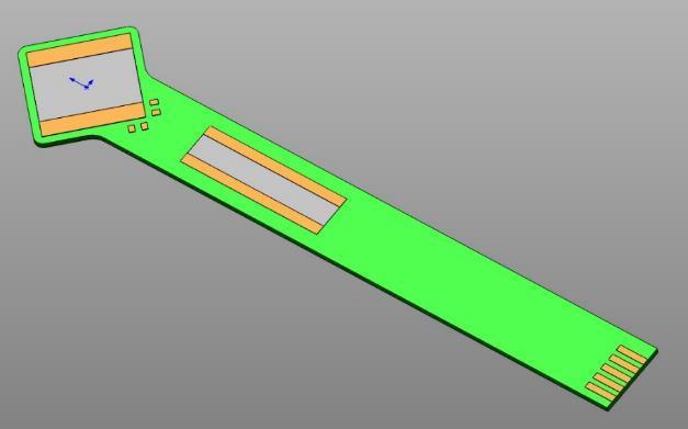
Thin Film Resistor Integration into Flex-Boards
 Thin Film Resistor Integration into Flex-Boards 7 rd International Workshop Flexible Electronic Systems November 29, 2006, Munich by Dr. Hans Burkard Hightec H MC AG, Lenzburg, Switzerland 1 Content HiCoFlex:
FPGA World Conference Stockholm 08 September John Steinar Johnsen -Josse- Senior Technical Advisor
 FPGA World Conference Stockholm 08 September 2015 John Steinar Johnsen -Josse- Senior Technical Advisor Agenda FPGA World Conference Stockholm 08 September 2015 - IPC 4101C Materials - Routing out from
Antenna Matching Within an Enclosure Part II: Practical Techniques and Guidelines
 Antenna Matching Within an Enclosure Part II: Practical Techniques and Guidelines By Johnny Lienau, RF Engineer June 2012 Antenna selection and placement can be a difficult task, and the challenges of
PCB technologies and manufacturing General Presentation
 PCB technologies and manufacturing General Presentation 1 Date : December 2014 3 plants for a global offer dedicated to the European market and export Special technologies, Harsh environment PCB for space
Michael R. Creeden CEO/CID+ San Diego PCB, Inc. & EPTAC (858)
") Michael R. Creeden CEO/CID+ San Diego PCB, Inc. & EPTAC mike.creeden@sdpcb.com (858)271-5722 1. Why we collaborate? 2. When do we collaborate? 3. Who do we collaborate with? 4. What do we collaborate?
Michael R. Creeden CEO/CID+ San Diego PCB, Inc. & EPTAC mike.creeden@sdpcb.com (858)271-5722 1. Why we collaborate? 2. When do we collaborate? 3. Who do we collaborate with? 4. What do we collaborate?
Manufacture and Performance of a Z-interconnect HDI Circuit Card Abstract Introduction
 Manufacture and Performance of a Z-interconnect HDI Circuit Card Michael Rowlands, Rabindra Das, John Lauffer, Voya Markovich EI (Endicott Interconnect Technologies) 1093 Clark Street, Endicott, NY 13760
How to anticipate Signal Integrity Issues: Improve my Channel Simulation by using Electromagnetic based model
 How to anticipate Signal Integrity Issues: Improve my Channel Simulation by using Electromagnetic based model HSD Strategic Intent Provide the industry s premier HSD EDA software. Integration of premier
ABA GHz Broadband Silicon RFIC Amplifier. Application Note 1349
 ABA-52563 3.5 GHz Broadband Silicon RFIC Amplifier Application Note 1349 Introduction Avago Technologies ABA-52563 is a low current silicon gain block RFIC amplifier housed in a 6-lead SC 70 (SOT- 363)
BGA (Ball Grid Array)
") BGA (Ball Grid Array) National Semiconductor Application Note 1126 November 2002 Table of Contents Introduction... 2 Package Overview... 3 PBGA (PLASTIC BGA) CONSTRUCTION... 3 TE-PBGA (THERMALLY ENHANCED
BGA (Ball Grid Array) National Semiconductor Application Note 1126 November 2002 Table of Contents Introduction... 2 Package Overview... 3 PBGA (PLASTIC BGA) CONSTRUCTION... 3 TE-PBGA (THERMALLY ENHANCED
Sectional Design Standard for High Density Interconnect (HDI) Printed Boards
 Printed Boards") IPC-2226 ASSOCIATION CONNECTING ELECTRONICS INDUSTRIES Sectional Design Standard for High Density Interconnect (HDI) Printed Boards Developed by the HDI Design Subcommittee (D-41) of the HDI Committee
IPC-2226 ASSOCIATION CONNECTING ELECTRONICS INDUSTRIES Sectional Design Standard for High Density Interconnect (HDI) Printed Boards Developed by the HDI Design Subcommittee (D-41) of the HDI Committee
INVENTION DISCLOSURE- ELECTRONICS SUBJECT MATTER IMPEDANCE MATCHING ANTENNA-INTEGRATED HIGH-EFFICIENCY ENERGY HARVESTING CIRCUIT
 INVENTION DISCLOSURE- ELECTRONICS SUBJECT MATTER IMPEDANCE MATCHING ANTENNA-INTEGRATED HIGH-EFFICIENCY ENERGY HARVESTING CIRCUIT ABSTRACT: This paper describes the design of a high-efficiency energy harvesting
Plane Crazy, Part 2 BEYOND DESIGN. by Barry Olney
 by Barry Olney column BEYOND DESIGN Plane Crazy, Part 2 In my recent four-part series on stackup planning, I described the best configurations for various stackup requirements. But I did not have the opportunity
TD-DEV V Technical Specification
 High-Efficiency MODULE Carrier Board TD-DEV-500-12V Technical Specification POWER SUPPLY TECHNOLOGY FEATURES Low profile 1U, 500W power supply High efficiency power supply Fully integrated with CPU control
Application Note 5011
 MGA-62563 High Performance GaAs MMIC Amplifier Application Note 511 Application Information The MGA-62563 is a high performance GaAs MMIC amplifier fabricated with Avago Technologies E-pHEMT process and
MMIC: Introduction. Evangéline BENEVENT. Università Mediterranea di Reggio Calabria DIMET
 Evangéline BENEVENT Università Mediterranea di Reggio Calabria DIMET 1 Evolution of electronic circuits: high frequency and complexity Moore s law More than Moore System-In-Package System-On-Package Applications
Application Note 5012
 MGA-61563 High Performance GaAs MMIC Amplifier Application Note 5012 Application Information The MGA-61563 is a high performance GaAs MMIC amplifier fabricated with Avago Technologies E-pHEMT process and
MICROELECTRONICS ASSSEMBLY TECHNOLOGIES. The QFN Platform as a Chip Packaging Foundation
 West Coast Luncheon January 15, 2014. PROMEX PROMEX INDUSTRIES INC. MICROELECTRONICS ASSSEMBLY TECHNOLOGIES The QFN Platform as a Chip Packaging Foundation 3075 Oakmead Village Drive Santa Clara CA Ɩ 95051
Wide-Band Two-Stage GaAs LNA for Radio Astronomy
 Progress In Electromagnetics Research C, Vol. 56, 119 124, 215 Wide-Band Two-Stage GaAs LNA for Radio Astronomy Jim Kulyk 1,GeWu 2, Leonid Belostotski 2, *, and James W. Haslett 2 Abstract This paper presents
PCB Layout Techniques of Buck Converter
 Switching Regulator Series PCB ayout Techniques of Buck Converter PCB layout design for switching power supply is as important as the circuit design. Appropriate layout can avoid various problems caused
Integrated Circuits: FABRICATION & CHARACTERISTICS - 4. Riju C Issac
 Integrated Circuits: FABRICATION & CHARACTERISTICS - 4 Riju C Issac INTEGRATED RESISTORS Resistor in a monolithic IC is very often obtained by the bulk resistivity of one of the diffused areas. P-type
DESIGNING A PATCH ANTENNA FOR DOPPLER SYSTEMS
 DESIGNING A PATCH ANTENNA FOR DOPPLER SYSTEMS Doppler Requirements for Antennas Range Determines power consumption Defines frequency band R max = 4 P t GσA e 4π 2 S min Narrow Bandwidth Tolerance range
Application Bulletin 240
 Application Bulletin 240 Design Consideration CUSTOM CAPABILITIES Standard PC board fabrication flexibility allows for various component orientations, mounting features, and interconnect schemes. The starting
Electrical Testing of Passive Components
 feature Electrical Testing of Passive Components by Todd L. Kolmodin, Manfred Ludwig, Howard Carpenter and Rick Meraw Gardien Services USA and China Introduction Substrates have become more critical with
Electrical Specifications. Maximum Maximum Resistance Working Overload Temperature. Mechanical Specifications
 Features: Thin Film Technology for precision and stability Excellent power to size ratio Exhibits good pulse power characteristics RoHS compliant / lead-free Type / Code MLF12 0207 MLFM1 Package Size 0207
tuning and RF circuits wireless automotive inductors inductance (L). Now frequencies
. Now frequencies") RF Chip Inductor Applications December 2011 Application Note RF chip are an integral part of many tuning and filtering circuits and are mainly used in the RF circuits in electronics systems. With a small
RF Chip Inductor Applications December 2011 Application Note RF chip are an integral part of many tuning and filtering circuits and are mainly used in the RF circuits in electronics systems. With a small
Application Note 5525
 Using the Wafer Scale Packaged Detector in 2 to 6 GHz Applications Application Note 5525 Introduction The is a broadband directional coupler with integrated temperature compensated detector designed for
CAD Layout Recommendations for the PowerBlox Family
 Solved by APPLICATION NOTE ANP4 TM CAD Layout Recommendations for the PowerBlox Family Introduction The Sipex PowerBlox family of parts offers designers a very high power density solution for wide input
New Materials and Method for Laser Trimmable NTC Thermistors
 New Materials and Method for Laser Trimmable NTC Thermistors By David J. Nabatian Gene A. Perschnick Chuck Rosenwald KOARTAN EMC Technology Corporation Artek Corporation Microelectronic Interconnect Materials
PI3DPX1207B Layout Guideline. Table of Contents. 1 Layout Design Guideline Power and GROUND High-speed Signal Routing...
 PI3DPX1207B Layout Guideline Table of Contents 1 Layout Design Guideline... 2 1.1 Power and GROUND... 2 1.2 High-speed Signal Routing... 3 2 PI3DPX1207B EVB layout... 8 3 Related Reference... 8 Page 1
Data Sheet. VMMK GHz Positive Gain Slope Low Noise Amplifier in SMT Package. Features. Description
 VMMK-3603 1-6 GHz Positive Gain Slope Low Noise Amplifier in SMT Package Data Sheet Description The VMMK-3603 is a small and easy-to-use, broadband, positive gain slope low noise amplifier operating in
Low-Cost PCB Design 1
 Low-Cost PCB Design 1 PCB design parameters Defining PCB design parameters begins with understanding: End product features, uses, environment, and lifetime goals PCB performance, manufacturing, and yield
Lab Hints. How to reduce the degree of effort in testing lab assignments GENERAL WIRING PARASITICS... 2 OSCILLATION... 3
 Lab Hints How to reduce the degree of effort in testing lab assignments GENERAL WIRING PARASITICS... 2 OSCILLATION... 3 COUPLING & OSCILLATION DUE TO SLOPPY WIRING ON THE BENCH... 3 SHARING OF GROUND CONNECTIONS
EEE 161 Applied Electromagnetics Laboratory 7 Microstrip Lines and PCB fabrication
 Dr. Milica Markovic Applied Electromagnetics Laboratory page 1 EEE 161 Applied Electromagnetics Laboratory 7 Microstrip Lines and PCB fabrication Part I. Design an impedance matching circuit using actual
SiP packaging technology of intelligent sensor module. Tony li
 SiP packaging technology of intelligent sensor module Tony li 2016.9 Contents What we can do with sensors Sensor market trend Challenges of sensor packaging SiP technology to overcome challenges Overview
Microwave Characterization and Modeling of Multilayered Cofired Ceramic Waveguides
 Microwave Characterization and Modeling of Multilayered Cofired Ceramic Waveguides Microwave Characterization and Modeling of Multilayered Cofired Ceramic Waveguides Daniel Stevens and John Gipprich Northrop
5. The Different Types of Resistors
 5. The Different Types of Resistors Resistors ( R ), are the most fundamental and commonly used of all the electronic components, to the point where they are almost taken for granted. There are many different
Course Introduction. Content: 19 pages 3 questions. Learning Time: 30 minutes
 Course Introduction Purpose: This course discusses techniques that can be applied to reduce problems in embedded control systems caused by electromagnetic noise Objectives: Gain a basic knowledge about
Practical Measurements of Dielectric Constant and Loss for PCB Materials at High Frequency
 8 th Annual Symposium on Signal Integrity PENN STATE, Harrisburg Center for Signal Integrity Practical Measurements of Dielectric Constant and Loss for PCB Materials at High Frequency Practical Measurements
AN4630. PCB design guidelines for the BlueNRG and BlueNRG-MS devices. Application note. Introduction
 Application note PCB design guidelines for the BlueNRG and BlueNRG-MS devices Introduction The BlueNRG and BlueNRG-MS are very low power Bluetooth low energy (BLE) single-mode network processor devices,
Introduction: Planar Transmission Lines
 Chapter-1 Introduction: Planar Transmission Lines 1.1 Overview Microwave integrated circuit (MIC) techniques represent an extension of integrated circuit technology to microwave frequencies. Since four
What is New about Thin Laminates in 2013?
 PCBDesign 007 QuietPower column What is New about Thin Laminates in 2013? Istvan Novak, Oracle, February 2013 It is almost two years ago that the QuietPower column Thin Laminates: Buried Capacitance or
Evaluation of Package Properties for RF BJTs
 Application Note Evaluation of Package Properties for RF BJTs Overview EDA simulation software streamlines the development of digital and analog circuits from definition of concept and estimation of required
Using LME49810 to Build a High-Performance Power Amplifier Part I
 Using LME49810 to Build a High-Performance Power Amplifier Part I Panson Poon Introduction Although switching or Class-D amplifiers are gaining acceptance to audiophile community, linear amplification
PRINTED ELECTRONICS TECHNOLOGIES
 PRINTED ELECTRONICS TECHNOLOGIES YEARS OF R&D DRIVEN BY CONTINUOUS INNOVATION HAVE POSITIONNED GGI SOLUTIONS AS A LEADER IN PRINTED ELECTRONICS TECHNOLOGIES 2 As a level 1 member of the Printable Electronics
Surface Mount RF PIN Low Distortion Attenuator Diodes. Technical Data. HSMP-381x Series and HSMP-481x Series. Features
 Surface Mount RF PIN Low Distortion Attenuator Diodes Technical Data HSMP-81x Series and HSMP-481x Series Features Diodes Optimized for: Low Distortion Attenuating Microwave Frequency Operation Surface
Top View (Near-side) Side View Bottom View (Far-side) .89±.08. 4x.280. Orientation Marker Orientation Marker.
 Side View Bottom View (Far-side) .89±.08. 4x.280. Orientation Marker Orientation Marker.") Model B2F2AHF Ultra Low Profile 168 Balun Ω to 2Ω Balanced Description The B2F2AHF is a low profile sub-miniature balanced to unbalanced transformer designed for differential input locations on data conversion
Model B2F2AHF Ultra Low Profile 168 Balun Ω to 2Ω Balanced Description The B2F2AHF is a low profile sub-miniature balanced to unbalanced transformer designed for differential input locations on data conversion
TECHNICAL REPORT: CVEL Parasitic Inductance Cancellation for Filtering to Chassis Ground Using Surface Mount Capacitors
 TECHNICAL REPORT: CVEL-14-059 Parasitic Inductance Cancellation for Filtering to Chassis Ground Using Surface Mount Capacitors Andrew J. McDowell and Dr. Todd H. Hubing Clemson University April 30, 2014
NIRMA UNIVERSITY INSTITUTE OF TECHNOLOGY ELECTRICAL ENGINEERING DEPARTMENT EE101: Elements of Electrical Engineering DC CIRCUIT
 NIRMA UNIVERSITY INSTITUTE OF TECHNOLOGY ELECTRICAL ENGINEERING DEPARTMENT EE101: Elements of Electrical Engineering DC CIRCUIT Learning Objective: Resistance, Effect of temperature on resistance, temperature
Microcircuit Electrical Issues
 Microcircuit Electrical Issues Distortion The frequency at which transmitted power has dropped to 50 percent of the injected power is called the "3 db" point and is used to define the bandwidth of the
MicroSiP TM DC/DC Converters Fully Integrated Power Solutions
 MicroSiP TM DC/DC Converters Fully Integrated Power Solutions PicoStar TM Christophe Vaucourt Thies Puchert, Udo Ottl, Frank Stepniak, Florian Feckl 1 Outline Illustrate TI s recent developments in the
Application Note 1360
 ADA-4743 +17 dbm P1dB Avago Darlington Amplifier Application Note 1360 Description Avago Technologies Darlington Amplifier, ADA-4743 is a low current silicon gain block RFIC amplifier housed in a 4-lead
DL-150 The Ten Habits of Highly Successful Designers. or Design for Speed: A Designer s Survival Guide to Signal Integrity
 Slide -1 Ten Habits of Highly Successful Board Designers or Design for Speed: A Designer s Survival Guide to Signal Integrity with Dr. Eric Bogatin, Signal Integrity Evangelist, Bogatin Enterprises, www.bethesignal.com
Hardware Design Considerations for MKW41Z/31Z/21Z BLE and IEEE Device
 NXP Semiconductors Document Number: AN5377 Application Note Rev. 2, Hardware Design Considerations for MKW41Z/31Z/21Z BLE and IEEE 802.15.4 Device 1. Introduction This application note describes Printed
TC600. Enhanced Thermal Conductivity Ceramic Filled PTFE/Woven Fiberglass Laminate for Microwave Printed Circuit Boards
 MICROWAVE MATERIALS Enhanced Thermal Conductivity Ceramic Filled PTFE/Woven Fiberglass Laminate for Microwave Printed Circuit Boards Features: Best in Class Thermal Conductivity and Dielectric Constant
MA4AGSW2. AlGaAs SP2T PIN Diode Switch. MA4AGSW2 Layout. Features. Description. Absolute Maximum Ratings TA = +25 C (Unless otherwise specified)
") AlGaAs SP2T PIN Diode Switch Features Ultra Broad Bandwidth: 5 MHz to 5 GHz Functional bandwidth : 5 MHz to 7 GHz.7 db Insertion Loss, 33 db Isolation at 5 GHz Low Current consumption: -1 ma for Low Loss
AlGaAs SP2T PIN Diode Switch Features Ultra Broad Bandwidth: 5 MHz to 5 GHz Functional bandwidth : 5 MHz to 7 GHz.7 db Insertion Loss, 33 db Isolation at 5 GHz Low Current consumption: -1 ma for Low Loss
Optimization of Wafer Level Test Hardware using Signal Integrity Simulation
 June 7-10, 2009 San Diego, CA Optimization of Wafer Level Test Hardware using Signal Integrity Simulation Jason Mroczkowski Ryan Satrom Agenda Industry Drivers Wafer Scale Test Interface Simulation Simulation
DESIGN FOR MANUFACTURABILITY (DFM)
") T H A N K S F O R A T T E N D I N G OUR TECHNICAL WEBINAR SERIES DESIGN FOR MANUFACTURABILITY (DFM) Presented by: We don t just sell PCBs. We sell sleep. Cirtech EDA is the exclusive SA representative
T H A N K S F O R A T T E N D I N G OUR TECHNICAL WEBINAR SERIES DESIGN FOR MANUFACTURABILITY (DFM) Presented by: We don t just sell PCBs. We sell sleep. Cirtech EDA is the exclusive SA representative
Using Embedded Capacitance to Improve Electrical Performance, Eliminate Capacitors and Reduce Board Size in High Speed Digital and RF Applications
 Using Embedded Capacitance to Improve Electrical Performance, Eliminate Capacitors and Reduce Board Size in High Speed Digital and RF Applications Joel S. Peiffer 3M Company 3M Center, MS: 201-1E-21 St.
The Basics of Patch Antennas, Updated
 The Basics of Patch Antennas, Updated By D. Orban and G.J.K. Moernaut, Orban Microwave Products www.orbanmicrowave.com Introduction This article introduces the basic concepts of patch antennas. We use
3. Details on microwave PCB-materials like {ε r } etc. can be found in the Internet with Google for example: microwave laminates comparison.
 1. Introduction 1. As widely known for microwave PCB-design it is essential to obey the electromagnetic laws. RF-impedance matching therefore is a must. For the following steps one of the following tools
SMT Module RF Reference Design Guide. AN_ SMT Module RF Reference Design Guide _V1.01
 SMT Module RF Reference Design Guide AN_ SMT Module RF Reference Design Guide _V1.01 Document Title: SMT Module RF Reference Design Guide Version: 1.01 Date: 2010-2-10 Status: Document Control ID: Release
Pin Connections and Package Marking. GUx
 Surface Mount RF PIN Switch Diodes Technical Data HSMP-389x Series HSMP-89x Series Features Unique Configurations in Surface Mount Packages Add Flexibility Save Board Space Reduce Cost Switching Low Capacitance
PI3HDMIxxx 4-Layer PCB Layout Guideline for HDMI Products
 PI3HDMIxxx 4-Layer PCB Layout Guideline for HDMI Products Introduction The differential trace impedance of HDMI is specified at 100Ω±15% in Test ID 8-8 in HDMI Compliance Test Specification Rev.1.2a and
A 6 : 1 UNEQUAL WILKINSON POWER DIVIDER WITH EBG CPW
 Progress In Electromagnetics Research Letters, Vol. 8, 151 159, 2009 A 6 : 1 UNEQUAL WILKINSON POWER DIVIDER WITH EBG CPW C.-P. Chang, C.-C. Su, S.-H. Hung, and Y.-H. Wang Institute of Microelectronics,
Anaren 0805 (B0809J50ATI) balun optimized for Texas Instruments CC1100/CC1101 Transceiver
 balun optimized for Texas Instruments CC1100/CC1101 Transceiver") (ANN-2005) Rev B Page 1 of 13 Anaren 0805 (B0809J50ATI) balun optimized for Texas Instruments CC1100/CC1101 Transceiver Trong N Duong RF Co-Op Nithya R Subramanian RF Engineer Introduction The tradeoff
(ANN-2005) Rev B Page 1 of 13 Anaren 0805 (B0809J50ATI) balun optimized for Texas Instruments CC1100/CC1101 Transceiver Trong N Duong RF Co-Op Nithya R Subramanian RF Engineer Introduction The tradeoff
The Design of A 125W L-Band GaN Power Amplifier
 Sheet Code RFi0613 White Paper The Design of A 125W L-Band GaN Power Amplifier This paper describes the design and evaluation of a single stage 125W L-Band GaN Power Amplifier using a low-cost packaged
APPLICATION NOTE. System Design for RF Immunity
 APPLICATION NOTE System Design for RF Immunity Audio Codec Application Note Rev1.0 Page 1 of 6 March 2008 With the growth of the portable electronic devices industry, radiated RF fields and potential interference
What the Designer needs to know
 White Paper on soldering QFN packages to electronic assemblies. Brian J. Leach VP of Sales and Marketing AccuSpec Electronics, LLC Defect free QFN Assembly What the Designer needs to know QFN Description:
Silicon Interposers enable high performance capacitors
 Interposers between ICs and package substrates that contain thin film capacitors have been used previously in order to improve circuit performance. However, with the interconnect inductance due to wire
PCB DESIGN AND ASSEMBLY FOR POWER SUPPLIES
 PCB DESIGN AND ASSEMBLY FOR POWER SUPPLIES Power supplies come in large varieties, can have different topologies, and feature numerous safeguards. Design of printed circuit boards (PCBs) for powers supplies
Features. Preliminary. = +25 C, IF = 1 GHz, LO = +13 dbm*
 Typical Applications Features The is ideal for: Test Equipment & Sensors Point-to-Point Radios Point-to-Multi-Point Radios Military & Space Functional Diagram Wide IF Bandwidth: DC - 17 GHz Input IP3:
SERIES 100 & 200 AXIAL LEADED RESISTORS
 SERIES 100 & 200 AXIAL LEADED RESISTORS KANTHAL GLOBAR Non-inductive bulk ceramic resistor Uniform distribution of energy throughout resistor body Replacement of Carbon Composition Resistors Large peak
Thin-Film Directional Couplers
 DB6N 9 Couplers GENERAL DESCRIPTION RFAP TECHNOLOGY The DB6N 9 Coupler is based on thin-film multilayer technology. The technology provides a miniature part with excellent high frequency performance and
Top View (Near-side) Side View Bottom View (Far-side) ± ±.08. 4x.28. Orientation Marker Balanced port 1.
 Side View Bottom View (Far-side) ± ±.08. 4x.28. Orientation Marker Balanced port 1.") Model BD2FAHF Ultra Low Profile 168 Balun Ω to Ω Balanced Description The BD2FAHF is a low profile sub-miniature balanced to unbalanced transformer designed for differential input locations on data conversion
Model BD2FAHF Ultra Low Profile 168 Balun Ω to Ω Balanced Description The BD2FAHF is a low profile sub-miniature balanced to unbalanced transformer designed for differential input locations on data conversion
AN4819 Application note
 Application note PCB design guidelines for the BlueNRG-1 device Introduction The BlueNRG1 is a very low power Bluetooth low energy (BLE) single-mode system-on-chip compliant with Bluetooth specification
Static Phase Range Enhancement of Reflectarray Resonant Elements
 Proceedings of MUCEET2009 Malaysian Technical Universities Conference on Engineering and Technology June 20-22, 2009, MS Garden,Kuantan, Pahang, Malaysia Static Phase Range Enhancement of Reflectarray
WF12T, WF08T, WF06T, WF04T 0.5%, 0.1% TC50 High Precision Thin Film chip resistors Size 1206, 0805, 0603, 0402
 SPECIFICATION OF HIGH PRECISION THIN FILM CHIP RESISTOR Ver: Page: of 8 ROHS compliance WF2T, WF08T, WF06T, WF04T 0.5%, 0.% TC50 High Precision Thin Film chip resistors Size 206, 0805, 0603, 0402 SPECIFICATION
Matched Length Matched Delay
 by Barry Olney column BEYOND DESIGN Matched Delay In previous columns, I have discussed matched length routing and how matched length does not necessarily mean matched delay. But, all design rules, specified
Technology in Balance
 Technology in Balance A G1 G2 B Basic Structure Comparison Regular capacitors have two plates or electrodes surrounded by a dielectric material. There is capacitance between the two conductive plates within
Class-D Audio Power Amplifiers: PCB Layout For Audio Quality, EMC & Thermal Success (Home Entertainment Devices)
") Class-D Audio Power Amplifiers: PCB Layout For Audio Quality, EMC & Thermal Success (Home Entertainment Devices) Stephen Crump http://e2e.ti.com Audio Power Amplifier Applications Audio and Imaging Products
Class-D Audio Power Amplifiers: PCB Layout For Audio Quality, EMC & Thermal Success (Home Entertainment Devices) Stephen Crump http://e2e.ti.com Audio Power Amplifier Applications Audio and Imaging Products
Design and Analysis of Wilkinson Power Divider Using Microstrip Line and Coupled Line Techniques
 IOSR Journal of Electronics and Communication Engineering (IOSR-JECE) e-issn: 2278-2834,p-ISSN: 2278-8735 PP 34-40 www.iosrjournals.org Design and Analysis of Wilkinson Power Divider Using Microstrip Line
DATA SHEET THICK FILM CHIP RESISTORS Introduction
 DATA SHEET THICK FILM CHIP RESISTORS Introduction Product Specification December 5, 2017 V.8 Product specification 2 Data in data sheets is presented - whenever possible -according to a 'format', in which
High Frequency Single & Multi-chip Modules based on LCP Substrates
 High Frequency Single & Multi-chip Modules based on Substrates Overview Labtech Microwave has produced modules for MMIC s (microwave monolithic integrated circuits) based on (liquid crystal polymer) substrates
Applications of Solder Fortification with Preforms
 Applications of Solder Fortification with Preforms Carol Gowans Indium Corporation Paul Socha Indium Corporation Ronald C. Lasky, PhD, PE Indium Corporation Dartmouth College ABSTRACT Although many have
Common myths, fallacies and misconceptions in Electromagnetic Compatibility and their correction.
 Common myths, fallacies and misconceptions in Electromagnetic Compatibility and their correction. D. A. Weston EMC Consulting Inc 22-3-2010 These are some of the commonly held beliefs about EMC which are
Design and Demonstration of a Passive, Broadband Equalizer for an SLED Chris Brinton, Matthew Wharton, and Allen Katz
 Introduction Design and Demonstration of a Passive, Broadband Equalizer for an SLED Chris Brinton, Matthew Wharton, and Allen Katz Wavelength Division Multiplexing Passive Optical Networks (WDM PONs) have
Welcome to Yageo Chip Resistor training module. This module will provide an overview of chip resistor introduction, including single chip, array,
 1 Welcome to Yageo Chip Resistor training module. This module will provide an overview of chip resistor introduction, including single chip, array, network for both general use and automotive grade. Also,
Application Information
 Application Information Secrets of Measuring Currents Above 50 Amps By Georges El Bacha, Evan Shorman, and Harry Chandra, Introduction It can be challenging to sense currents exceeding 50 A because the
Making Sense of Laminate Dielectric Properties By Michael J. Gay and Richard Pangier Isola
 Making Sense of Laminate Dielectric Properties By Michael J. Gay and Richard Pangier Isola Abstract System operating speeds continue to increase as a function of the consumer demand for such technologies