Improve SMT Assembly Yields Using Root Cause Analysis in Stencil Design
|
|
|
- Lora Hood
- 6 years ago
- Views:
Transcription
1 Improve SMT Assembly Yields Using Root Cause Analysis in Stencil Design Greg Smith FCT Assembly, Inc. This paper and presentation was first presented at the 2017 IPC Apex Expo Technical Conference and published in the 2017 Technical Conference Proceedings.
2 Introduction Outline Root cause analysis to improve defects through stencil design Solder paste release (transfer efficiency) Solder-balls (mid chip solder beads) Tombstoning Bridging at print Bridging at SMT reflow Insufficient solder volume at SMT reflow Voiding Conclusions
3 Introduction Bridging at Print Bridging at Reflow Paste Release Voiding Tombstones

4 Root Cause Analysis to Improve Solder Paste Release IPC 7525B recommends 0.66 area ratio for acceptable solder paste release Area ratio considers stencil thickness and aperture area Question: Does the size of the PWB SMT land pad affect solder paste release?

5 Root Cause Analysis to Improve Solder Paste Release PWB designers modify the lines, traces and pads to allow for etch back As copper weights increase PWB land pads become smaller than nominal Non-uniform surface coatings such as HASL affect the contact surface
6 Root Cause Analysis to Improve Solder Paste Release Actual PWB Cross Section Measurement Cu Weight Surface Finish Surface Measurement (in) Nominal Trace Width (in) Difference- Surface vs Nominal (in) Foot Measurement (in) 2 oz HASL oz HASL oz ENIG oz HASL oz HASL oz ENIG oz ENIG Should a new modified surface area ratio be used to predict acceptable printing for small components?

7 Root Cause Analysis to Improve Solder Paste Release The modified comparison (surface area ratio) uses actual SMT pad surface Heavier copper weights will produce larger reductions at the surface Flat surface finishes, like ENIG, do not change the size of the surface An additional reduction is made on non-flat surface finishes, like HASL
8 Root Cause Analysis to Improve Solder Paste Release Copper Weight (oz) Copper Thickness (µm) Size Reduction (inches) Size Reduction inches with ENIG, OSP, Ag, Sn Size Reduction (inches) with HASL Utilizing these SMT pad size reductions may provide a more realistic representation of what SMT pad sizes to expect on physical PCBs. The modified surface area ratio will be used to test this theory. Component Copper Weight Surface Finish PWB Pad Size Stencil Aperture Size Area Ratio Surface Area Ratio.4 BGA 2 oz HASL 9 mil Round 9 mil Round BGA 2 oz HASL 9 mil Round 11 mil Sq, 2 mil Radius ubga 2 oz HASL 11 mil Round 9 mil Sq, 2 mil Radius ubga 2 oz HASL 11 mil Round 11 mil Round mil Sq, 2 mil ubga 2 oz HASL 11 mil Round Radius

9 Root Cause Analysis to Improve Solder Paste Release Two 4 mil thick stencils were used: un-coated and coated with a Flouro-Polymer Nano Coating (FPN). Component Group PWB Pad Size Stencil Aperture Size.5 BGA 1 12 mil Round 10 mil Sq, 2 mil Radius.5 BGA 2 12 mil Round 12 mil Round.5 BGA 3 12 mil Round 14 mil Sq, 2 mil Radius.4 BGA 1 9 mil Round 7 mil Sq, 2 mil Radius.4 BGA 2 9 mil Round 9 mil Round.4 BGA 3 9 mil Round 11 mil Sq, 2 mil Radius x 11.8 mils 5.9 x 9.8, 2 mil Radius x 11.8 mils 7.9 x 11.8, 2 mil Radius x 11.8 mils 7.9 x 9, 2 mil Radius x 9.8 mils 13.7 x 7.8, 2 mil Radius x 9.8 mils 15.7 x 9.8, 2 mil Radius x 9.8 mils 14.7 x 8.8, 2 mil Radius ubga 1 11 mil Round 9 mil Sq, 2 mil Radius ubga 2 11 mil Round 11 mil Round ubga 3 11 mil Round 13 mil Sq, 2 mil Radius ubga 4 11 mil Round 15 mil Sq, 2 mil Radius QFN x 9.8 Oblong 55.4 x 9.8, Oblong QFN x 9.8 Oblong 35.4 x 9.8, Oblong QFN x 9.8 Oblong 65.4 x 7.8, Oblong
10 Root Cause Analysis to Improve Solder Paste Release Experiment: 5 Boards, 2 oz Cu, HASL printed with No Clean SAC305, Type 4 Paste 5 Boards, 2 oz Cu, HASL printed with Water Soluble SAC305, Type 3 Paste 5 Boards, 1 oz Cu, ENIG printed with No Clean SAC305, Type 4 Paste 5 Boards, 1 oz Cu, HASL printed with No Clean SAC305, Type 4 Paste All solder paste bricks measured using 3D, SPI to obtain volume and calculate transfer efficiency
11 Root Cause Analysis to Improve Solder Paste Release As area ratio increases, transfer efficiency increases in a linear fashion As surface area ratio increases, transfer efficiency does not increase in a linear fashion
12 Root Cause Analysis to Improve Solder Paste Release 46 Pin ubga Data Calculating surface area ratio based on copper weight of the outer layer and the surface finish on the board is not a good method to predict transfer efficiency.
13 Root Cause Analysis to Improve Solder Paste Release Results and Recommendations for Improving Paste Release Area Ratio is best method to predict Transfer Efficiency FPN coatings allow lower Area Ratios to achieve same Transfer Efficiency

14 Root Cause Analysis to Improve Solder Paste Release Results and Recommendations for Improving Paste Release-Small Apertures 4 Mil Stencil; No Clean SAC 305 T4 Paste, All board types 50% Transfer Efficiency Uncoated: Approx area ratio FPN Coated: Approx area ratio 30% Transfer Efficiency Uncoated: Approx area ratio FPN Coated: Approx area ratio

15 Root Cause Analysis to Improve Solder Paste Release Results and Recommendations for Improving Paste Release-Small Apertures Another indicator of transfer efficiency is solder paste: Paste type and powder size play a role in TE Looking at FPN data, 0.53 area ratio component has 55% TE with NC Type 4, WS Type 3 paste releases at 28% TE This is dependent upon the solder paste used

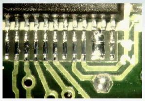
16 Solder-balls (Mid Chip Solder Beads): Stencil design to minimize solder balls Typically occurs on two pin discrete components Can be prevented or greatly reduced by stencil design. Root cause analysis of solder ball defects Compare design of stencil apertures to actual package Stencil apertures must fall in the correct location vs component leads

17 Solder-balls (Mid Chip Solder Beads): Stencil design to minimize solder balls The actual dimensions of part package are identified
18 The chip design must be overlaid onto the board land pads using a Gerber editor. Solder-balls (Mid Chip Solder Beads): Stencil design to minimize solder balls U Shape Aperture (7.5 Mil Minimum,>0201 s)
19 Solder-balls (Mid Chip Solder Beads): Stencil design to minimize solder balls Inv Homeplate Aperture (7.5 Mil Minimum,>0201 s) ALWAYS CALCULATE AREA RATIO WHEN CHANGING TO U SHAPE OR INVERTED HOMEPLATE APERTURES

20 Tombstoning: Improving tombstoning with stencil design Large stencil apertures/pwb land pads that extend further than half the length of component can create tombstoning Similar correction to solder balling. Outside of chip component should fall at midpoint of stencil apertures/pwb land pad.
21 Tombstoning: Improving tombstoning with stencil design (7.5 Mil Minimum,>0201 s) ALWAYS CALCULATE AREA RATIO WHEN CHANGING TO U SHAPE OR INVERTED HOMEPLATE APERTURES
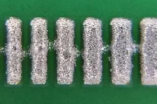
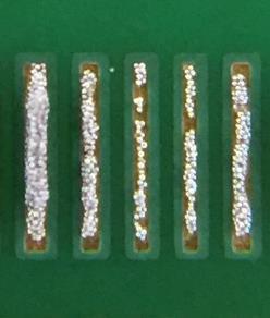
22 Bridging at Print: Simple guidelines to eliminate bridging Use Half Pitch Rule to determine aperture width. Leave length 1:1 with land pad. If land pad width is less than half pitch, leave aperture 1:1. On apertures larger than 33 mil (.84mm) pitch, reduce apertures to half pitch up to 20% maximum reduction. Use area ratio rule to determine acceptable thickness for stencil foil. There are no guarantees for poor board design.
23 Bridging at SMT Reflow: What causes bridging after reflow when it is not present after print? Most often seen on Gull Wing, QFP
.")
24 Bridging at SMT Reflow: What causes bridging after reflow when it is not present after print? Component data sheet is necessary. Identify foot dimension (Lp). If foot is 25% shorter or more than land pad, bridging can occur
25 Bridging at SMT Reflow: What causes bridging after reflow when it is not present after print? PWB land pad is designed for a specific component If the component is replaced by a different component with a shorter foot, then bridging at reflow can occur

26 Bridging at SMT Reflow: What causes bridging after reflow when it is not present after print? Component Foot vs Land Pad Volume Reduction of PWB Land 25% Shorter 10% 50% Shorter 25% 70% Shorter 40% New aperture to be centered on component foot

27 Insufficient Solder Volume at SMT Reflow: The correlation of stencil design to solder volume for leadless devices. Compare the leadless package termination size to the PCB land pad. Good: PCB land pad length is <110% of the leadless termination length Bad: PCB land pad length is more than 110% of termination length. Solder volume must be increased.

28 Insufficient Solder Volume at SMT Reflow: The correlation of stencil design to solder volume for leadless devices. Aperture widths should follow Half Pitch Rule. Additional solder paste volume should always be printed to the toe side. Stencil apertures can be extended up to 40 mils beyond SMT land pad toe. Typical is 5 10 mils beyond toe.

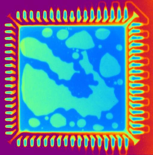
29 Voiding: Design ideas to reduce voiding on ground pads IPC 7525(B) Stencil Design Guidelines suggest 20% - 50% reduction in area, use of window pane design when possible and to avoid applying paste directly over vias. Window pane design used historically. Five dot pattern has been successfully used over past few years. Goal - to reduce voiding and remove volume to eliminate skew or twist
 Spacing in mils (mm) Paste Coverage Area (%) U9 Square 88 (2.24) 20 (0.51) 65.3 U10 Diamond 99 (2.51) 20 (0.51) 65.3 U11 Circle 132 (3.")
30 Voiding: Design ideas to reduce voiding on ground pads Stencil Design used to determine void percentage based on ground pad stencil design. Location Aperture Shape Aperture Size in mils (mm) Spacing in mils (mm) Paste Coverage Area (%) U9 Square 88 (2.24) 20 (0.51) 65.3 U10 Diamond 99 (2.51) 20 (0.51) 65.3 U11 Circle 132 (3.35) 8 (0.20) 63.9 U12 Stripe 40 (1.02) 20 (0.51) 65.0

31 Voiding: Design ideas to reduce voiding on ground pads 3 Different Water Soluble, SAC305 pastes printed 2 Different No Clean, SAC305 pastes printed Components placed and reflowed X-Ray Images taken and void percentage measured
32 Voiding: Design ideas to reduce voiding on ground pads Water soluble pastes (A, B, E) generate higher voiding than no cleans (C, D) WS paste A generated lowest voiding of the water solubles Stencil design had little impact on voiding levels

 was statistically")

33 Voiding: Design ideas to reduce voiding on ground pads Tukey-Kramer HSD used to validate results Voiding by stencil design (location) was statistically similar for each of these solder pastes. Stencil design made no difference in this test
.")
34 Voiding: Design ideas to reduce voiding on ground pads Tukey-Kramer HSD used to validate results For water soluble paste B, voiding was statistically higher for the 5 dot pattern (U11). The other designs were not statistically different.
35 Conclusions Identification of Universal defects in print process is critical to improve first pass yields. To prevent insufficient paste at print, stencil foil thickness must be chosen based on area ratios. The type of paste has an effect. Solder ball issues can be addressed using a U-Shape or Inverted Homeplate. Tombstoning can be reduced or eliminated with a Reverse U- Shape or Reverse Inverted Homeplate design.
36 Conclusions The Half Pitch Rule is a valid method to prevent bridging at print. When bridging after reflow is present, the size of the PWB land pad must be compared to the actual component lead and the stencil aperture size must be adjusted to remove volume. Reducing voiding on BTC ground pads is an ongoing challenge. Different stencil aperture designs were shown not to be statistically different in voiding results with the exception of one design on a specific paste.
37 Future Work Further investigation into ground pad designs for BTC's will be conducted to identify stencil patterns that can minimize voiding after reflow.

38 THANK YOU!
Improve SMT Assembly Yields Using Root Cause Analysis in Stencil Design
 Improve SMT Assembly Yields Using Root Cause Analysis in Stencil Design Greg Smith FCT Assembly, Inc. gsmith@fctassembly.com This paper and presentation was first presented at the 2017 IPC Apex Expo Technical
Improve SMT Assembly Yields Using Root Cause Analysis in Stencil Design
 Improve SMT Assembly Yields Using Root Cause Analysis in Stencil Design Greg Smith FCT Assembly, Inc. Greeley, CO Abstract Reduction of first pass defects in the SMT assembly process minimizes cost, assembly
Performance Enhancing Nano Coatings: Changing the Rules of Stencil Design. Tony Lentz
 Performance Enhancing Nano Coatings: Changing the Rules of Stencil Design Tony Lentz tlentz@fctassembly.com Outline/Agenda Introduction Experimental Design Results of Experiment Conclusions Acknowledgements
Step Stencil Technology
 Step Stencil Technology Greg Smith gsmith@fctassembly.com Tony Lentz tlentz@fctassembly.com Outline/Agenda Introduction Step Stencils Technologies Step Stencil Design Printing Experiment Experimental Results
Fill the Void IV: Elimination of Inter-Via Voiding
 Fill the Void IV: Elimination of Inter-Via Voiding Tony Lentz FCT Assembly Greeley, CO, USA Greg Smith BlueRing Stencils Lumberton, NJ, USA ABSTRACT Voids are a plague to our electronics and must be eliminated!
FILL THE VOID III. Tony Lentz FCT Assembly Greeley, CO, USA
 FILL THE VOID III Tony Lentz FCT Assembly Greeley, CO, USA tlentz@fctassembly.com ABSTRACT This study is part three in a series of papers on voiding in solder joints and methods for mitigation of voids.
Printing Practices for Components. Greg Smith
 Printing Practices for 01005 Components Greg Smith gsmith@fctassembly.com Outline/Agenda Introduction 01005 Components-Size, Shape and usage Stencil Design Transfer Efficiencies Q & A Introduction 01005
HOW DOES PRINTED SOLDER PASTE VOLUME AFFECT SOLDER JOINT RELIABILITY?
 HOW DOES PRINTED SOLDER PASTE VOLUME AFFECT SOLDER JOINT RELIABILITY? ABSTRACT Printing of solder paste and stencil technology has been well studied and many papers have been presented on the topic. Very
HOW DOES SURFACE FINISH AFFECT SOLDER PASTE PERFORMANCE?
 HOW DOES SURFACE FINISH AFFECT SOLDER PASTE PERFORMANCE? Tony Lentz FCT Assembly Greeley, CO, USA tlentz@fctassembly.com ABSTRACT The surface finishes commonly used on printed circuit boards (PCBs) have
What the Designer needs to know
 White Paper on soldering QFN packages to electronic assemblies. Brian J. Leach VP of Sales and Marketing AccuSpec Electronics, LLC Defect free QFN Assembly What the Designer needs to know QFN Description:
Stencil Technology: SMTA Carolinas Chapter & GMI 17Feb11 Bill Kunkle Manager Quality & Stencil Technology MET Associates Lumberton, NJ
 Stencil Technology: 2011 SMTA Carolinas Chapter & GMI 17Feb11 Bill Kunkle Manager Quality & Stencil Technology MET Associates Lumberton, NJ 1 Current Stencil Technology Summary Processes, Materials, Capabilities,
Broadband Printing: The New SMT Challenge
 Broadband Printing: The New SMT Challenge Rita Mohanty & Vatsal Shah, Speedline Technologies, Franklin, MA Gary Nicholls, Ron Tripp, Cookson Electronic Assembly Materials Engineered Products, Johnson City,
BOARD DESIGN, SURFACE MOUNT ASSEMBLY AND BOARD LEVEL RELIABILITY ASPECTS OF FUSIONQUAD TM PACKAGES
 BOARD DESIGN, SURFACE MOUNT ASSEMBLY AND BOARD LEVEL RELIABILITY ASPECTS OF FUSIONQUAD TM PACKAGES Ahmer Syed 1, Sundar Sethuraman 2, WonJoon Kang 1, Gary Hamming 1, YeonHo Choi 1 1 Amkor Technology, Inc.
Can Nano-Coatings Really Improve Stencil Performance? Tony Lentz FCT Assembly
 Can Nano-Coatings Really Improve Stencil Performance? Tony Lentz FCT Assembly tlentz@fctassembly.com Outline/Agenda Introduction Claims & questions about coatings Experiment design Results of coating performance
Can Nano-Coatings Really Improve Stencil Performance? Tony Lentz FCT Assembly
 Can Nano-Coatings Really Improve Stencil Performance? Tony Lentz FCT Assembly tlentz@fctassembly.com Outline/Agenda Introduction Claims & questions about coatings Experiment design Results of coating performance
TOLERANCE FORGOTTEN: IMPACTS OF TODAY S COMPONENT PACKAGING AND COPPER ROUTING ON ELECTRONIC
 TOLERANCE FORGOTTEN: IMPACTS OF TODAY S COMPONENT PACKAGING AND COPPER ROUTING ON ELECTRONIC Presented By: Dale Lee E-mail: Dale.Lee@Plexus.Com April 2013 High Layer Counts Wide Range Of Component Package
The Impact of Reduced Solder Alloy Powder Size on Solder Paste Print Performance. Presented by Karl Seelig, V.P. Technology AIM Metals & Alloys
 The Impact of Reduced Solder Alloy Powder Size on Solder Paste Print Performance Presented by Karl Seelig, V.P. Technology AIM Metals & Alloys Solder Powder Solder Powder Manufacturing and Classification
Understanding the Effect of Process Changes and Flux Chemistry on Mid-Chip Solder Balling
 As originally published in the IPC APEX EXPO Conference Proceedings. Understanding the Effect of Process Changes and Flux Chemistry on Mid-Chip Solder Balling Katherine Wilkerson, Ian J. Wilding, Michael
Ultra-Low Voiding Halogen-Free No-Clean Lead-Free Solder Paste for Large Pads
 Ultra-Low Voiding Halogen-Free No-Clean Lead-Free Solder Paste for Large Pads Li Ma, Fen Chen, and Dr. Ning-Cheng Lee Indium Corporation Clinton, NY mma@indium.com; fchen@indium.com; nclee@indium.com Abstract
Printing and Assembly Challenges for QFN Devices
 Printing and Assembly Challenges for QFN Devices Rachel Short Photo Stencil Colorado Springs Benefits and Challenges QFN (quad flatpack, no leads) and DFN (dual flatpack, no lead) are becoming more popular
CAN NANO-COATINGS REALLY IMPROVE STENCIL PERFORMANCE?
 CAN NANO-COATINGS REALLY IMPROVE STENCIL PERFORMANCE? Tony Lentz FCT Assembly Greeley, CO, USA tlentz@fctassembly.com ABSTRACT The trajectory of electronic design and its associated miniaturization shows
FINE TUNING THE STENCIL MANUFACTURING PROCESS AND OTHER STENCIL PRINTING EXPERIMENTS
 FINE TUNING THE STENCIL MANUFACTURING PROCESS AND OTHER STENCIL PRINTING EXPERIMENTS Chrys Shea Shea Engineering Services chrys@sheaengineering.com Ray Whittier Vicor Corporation VI Chip Division rwhittier@vicr.com
A review of the challenges and development of. the electronics industry
 SMTA LA/OC Expo, Long Beach, CA, USA A review of the challenges and development of SMT Wave and Rework assembly processes in SMT, the electronics industry Jasbir Bath, Consulting Engineer Christopher Associates
AltiumLive 2017: Creating Documentation for Successful PCB Manufacturing
 AltiumLive 2017: Creating Documentation for Successful PCB Manufacturing Julie Ellis TTM Field Applications Engineer Thomas Schneider Field Applications Engineer 1 Agenda 1 Complexity & Cost 2 3 4 5 6
DESIGN AND PROCESS DEVELOPMENT FOR THE ASSEMBLY OF PASSIVE COMPONENTS
 DESIGN AND PROCESS DEVELOPMENT FOR THE ASSEMBLY OF 01005 PASSIVE COMPONENTS J. Li 1, S. Poranki 1, R. Gallardo 2, M. Abtew 2, R. Kinyanjui 2, Ph.D., and K. Srihari 1, Ph.D. 1 Watson Institute for Systems
Optimization of Stencil Apertures to Compensate for Scooping During Printing.
 Optimization of Stencil Apertures to Compensate for Scooping During Printing. Gabriel Briceno, Ph. D. Miguel Sepulveda, Qual-Pro Corporation, Gardena, California, USA. ABSTRACT This study investigates
Print Performance Studies Comparing Electroform and Laser-Cut Stencils
 Print Performance Studies Comparing Electroform and Laser-Cut Stencils Rachel Miller Short William E. Coleman Ph.D. Photo Stencil Colorado Springs, CO Joseph Perault Parmi Marlborough, MA ABSTRACT There
Chrys Shea Shea Engineering Services. Originally presented at the IPC Conference on Soldering and Reliability, November 2013, Costa Mesa, CA
 Chrys Shea Shea Engineering Services Originally presented at the IPC Conference on Soldering and Reliability, November 2013, Costa Mesa, CA Introduction to Broadband (BB) Printing Traditional and New Approaches
What Can No Longer Be Ignored In Today s Electronic Designs. Presented By: Dale Lee
 What Can No Longer Be Ignored In Today s Electronic Designs Presented By: Dale Lee E-mail: Dale.Lee@Plexus.Com 24 January 2008 Introduction Component packaging technology continues to decrease in size
Stencil Printing of Small Apertures
 Stencil Printing of Small Apertures William E. Coleman Ph.D. Photo Stencil, Colorado Springs, CO Abstract Many of the latest SMT assemblies for hand held devices like cell phones present a challenge to
Bob Willis Process Guides
 What is a Printed Circuit Board Pad? What is a printed circuit board pad, it may sound like a dumb question but do you stop to think what it really does and how its size is defined and why? A printed circuit
inemi Statement of Work (SOW) Board Assembly TIG inemi Solder Paste Deposition Project
 Board Assembly TIG inemi Solder Paste Deposition Project") inemi Statement of Work (SOW) Board Assembly TIG inemi Solder Paste Deposition Project Version # 2.0 Date: 27 May 2008 Project Leader: Shoukai Zhang - Huawei Co-Project Leader: TC Coach: Basic Project
inemi Statement of Work (SOW) Board Assembly TIG inemi Solder Paste Deposition Project Version # 2.0 Date: 27 May 2008 Project Leader: Shoukai Zhang - Huawei Co-Project Leader: TC Coach: Basic Project
Selecting Stencil Technologies to Optimize Print Performance
 As originally published in the IPC APEX EXPO Conference Proceedings. Selecting Stencil Technologies to Optimize Print Performance Chrys Shea Shea Engineering Services Burlington, NJ USA Abstract The SMT
EVALUATION OF STENCIL TECHNOLOGY FOR MINIATURIZATION
 As originally published in the SMTA Proceedings EVALUATION OF STENCIL TECHNOLOGY FOR MINIATURIZATION Neeta Agarwal a Robert Farrell a Joe Crudele b a Benchmark Electronics Inc., Nashua, NH, USA b Benchmark
Engineering Manual LOCTITE GC 10 T3 Solder Paste
 Engineering Manual LOCTITE GC T Solder Paste Suitable for use with: Standard SAC Alloys GC The Game Changer Contents. Performance Summary. Introduction: Properties, Features & Benefits. Operating Parameters
APPLICATION NOTE 6381 ORGANIC LAND GRID ARRAY (OLGA) AND ITS APPLICATIONS
 AND ITS APPLICATIONS") Keywords: OLGA, SMT, PCB design APPLICATION NOTE 6381 ORGANIC LAND GRID ARRAY (OLGA) AND ITS APPLICATIONS Abstract: This application note discusses Maxim Integrated s OLGA and provides the PCB design and
Keywords: OLGA, SMT, PCB design APPLICATION NOTE 6381 ORGANIC LAND GRID ARRAY (OLGA) AND ITS APPLICATIONS Abstract: This application note discusses Maxim Integrated s OLGA and provides the PCB design and
SOLDER PASTE PRINTING DEFECT ANALYSIS AND PREVENTION (DVD-35C)
") This test consists of twenty multiple-choice questions. All questions are from the video: Solder Paste Printing Defect Analysis and Prevention (DVD-35C). Each question has only one most correct answer.
This test consists of twenty multiple-choice questions. All questions are from the video: Solder Paste Printing Defect Analysis and Prevention (DVD-35C). Each question has only one most correct answer.
Assembly Instructions for SCC1XX0 series
 Technical Note 82 Assembly Instructions for SCC1XX0 series TABLE OF CONTENTS Table of Contents...1 1 Objective...2 2 VTI's 32-lead Dual In-line Package (DIL-32)...2 3 DIL-32 Package Outline and Dimensions...2
M series. Product information. Koki no-clean LEAD FREE solder paste. Contents. Lead free SOLUTIONS you can TRUST.
 www.ko-ki.co.jp Ver. 42017e.2 Prepared on Oct. 26, 2007 Koki no-clean LEAD FREE solder paste Anti-Pillow Defect Product information This Product Information contains product performance assessed strictly
Assembly Instructions for SCA6x0 and SCA10x0 series
 Technical Note 71 Assembly Instructions for SCA6x0 and SCA10x0 series TABLE OF CONTENTS Table of Contents...1 1 Objective...2 2 VTI'S DIL-8 and DIL-12 packages...2 3 Package Outline and Dimensions...2
PLASMA STENCIL TREATMENTS: A STATISTICAL EVALUATION
 PLASMA STENCIL TREATMENTS: A STATISTICAL EVALUATION Matt Kelly, P.Eng. 1, William Green 2, Marie Cole 3, Ruediger Kellmann 4 IBM Corporation 1 Toronto, Canada; 2 Raleigh, NC, USA; 3 Fishkill, NY, USA;
AREA ARRAY TECHNOLOGY SYMPOSIUM
 AREA ARRAY TECHNOLOGY SYMPOSIUM Using SPI to Improve Print Yields Chrys Shea Shea Engineering Services/ CGI Americas Ray Whittier Vicor Corporation VI Chip Division SHEA ENGINEERING SERVICES Agenda How
PCB Supplier of the Best Quality, Lowest Price and Reliable Lead Time. Low Cost Prototype Standard Prototype & Production Stencil PCB Design
 The Best Quality PCB Supplier PCB Supplier of the Best Quality, Lowest Price Low Cost Prototype Standard Prototype & Production Stencil PCB Design Visit us: www. qualiecocircuits.co.nz OVERVIEW A thin
BGA (Ball Grid Array)
") BGA (Ball Grid Array) National Semiconductor Application Note 1126 November 2002 Table of Contents Introduction... 2 Package Overview... 3 PBGA (PLASTIC BGA) CONSTRUCTION... 3 TE-PBGA (THERMALLY ENHANCED
BGA (Ball Grid Array) National Semiconductor Application Note 1126 November 2002 Table of Contents Introduction... 2 Package Overview... 3 PBGA (PLASTIC BGA) CONSTRUCTION... 3 TE-PBGA (THERMALLY ENHANCED
TN016. PCB Design Guidelines for 5x5 DFN Sensors. Introduction. Package Marking
 PCB Design Guidelines for 5x5 DFN Sensors Introduction This technical note is intended to provide information about Kionix s 5 x 5 mm DFN (non wettable flank, i.e. standard) packages and guidelines for
Generic Multilayer Specifications for Rigid PCB s
 Generic Multilayer Specifications for Rigid PCB s 1.1 GENERAL 1.1.1 This specification has been developed for the fabrication of rigid SMT and Mixed Technology Multilayer Printed Circuit Boards (PCB's)
Chrys Shea Shea Engineering Services
 Chrys Shea Shea Engineering Services IMAPS New England 41 st Symposium and Expo May 6, 2014 PCB Layout DFM Feedback loop Component type, size, location Stencil Design Foil thickness, steps, aperture sizes
SMT Troubleshooting. Typical SMT Problems For additional process solutions, please refer to the AIM website troubleshooting guide
 SMT Troubleshooting Typical SMT Problems For additional process solutions, please refer to the AIM website troubleshooting guide Solder Balling Solder Beading Bridging Opens Voiding Tombstoning Unmelted
Prepared by Qian Ouyang. March 2, 2013
 AN075 Rework Process for TQFN Packages Rework Process for TQFN Packages Prepared by Qian Ouyang March 2, 2013 AN075 Rev. 1.1 www.monolithicpower.com 1 ABSTRACT MPS proprietary Thin Quad Flat package No
AN5046 Application note
 Application note Printed circuit board assembly recommendations for STMicroelectronics PowerFLAT packages Introduction The PowerFLAT package (5x6) was created to allow a larger die to fit in a standard
SMT Assembly Considerations for LGA Package
 SMT Assembly Considerations for LGA Package 1 Solder paste The screen printing quantity of solder paste is an key factor in producing high yield assemblies. Solder Paste Alloys: 63Sn/37Pb or 62Sn/36Pb/2Ag
S3X58-M High Reliability Lead Free Solder Paste. Technical Information. Koki no-clean LEAD FREE solder paste.
 www.ko-ki.co.jp #52007 Revised on Nov.27, 2014 Koki no-clean LEAD FREE solder paste High Reliability Lead Free Solder Paste S3X58-M500-4 Technical Information O₂ Reflowed 0.5mmP QFP 0603R This product
Investigating the Component Assembly Process Requirements
 Investigating the 01005-Component Assembly Process Requirements Rita Mohanty, Vatsal Shah, Arun Ramasubramani, Speedline Technologies, Franklin, MA Ron Lasky, Tim Jensen, Indium Corp, Utica, NY Abstract
TCLAD: TOOLS FOR AN OPTIMAL DESIGN
 TCLAD: TOOLS FOR AN OPTIMAL DESIGN THINGS TO CONSIDER WHEN DESIGNING CIRCUITS Many factors come into play in circuit design with respect to etching, surface finishing and mechanical fabrication processes;
Michael R. Creeden CEO/CID+ San Diego PCB, Inc. & EPTAC (858)
") Michael R. Creeden CEO/CID+ San Diego PCB, Inc. & EPTAC mike.creeden@sdpcb.com (858)271-5722 1. Why we collaborate? 2. When do we collaborate? 3. Who do we collaborate with? 4. What do we collaborate?
Michael R. Creeden CEO/CID+ San Diego PCB, Inc. & EPTAC mike.creeden@sdpcb.com (858)271-5722 1. Why we collaborate? 2. When do we collaborate? 3. Who do we collaborate with? 4. What do we collaborate?
Applications of Solder Fortification with Preforms
 Applications of Solder Fortification with Preforms Carol Gowans Indium Corporation Paul Socha Indium Corporation Ronald C. Lasky, PhD, PE Indium Corporation Dartmouth College ABSTRACT Although many have
& Anti-pillow. Product information. Koki no-clean LEAD FREE solder paste. Contents. Lead free SOLUTIONS you can TRUST.
 www.ko-ki.co.jp #46019E Revised on JUN 15, 2009 Koki no-clean LEAD FREE solder paste Super Low-Void & Anti-pillow Product information Pillow defect This Product Information contains product performance
Stencil Technology. Agenda: Laser Technology Stencil Materials Processes Post Process
 Stencil Technology Agenda: Laser Technology Stencil Materials Processes Post Process Laser s YAG LASER Conventional Laser Pulses Laser beam diameter is 2.3mil Ridges in the inside walls of the apertures
AN INVESTIGATION INTO THE DURABILITY OF STENCIL COATING TECHNOLOGIES
 AN INVESTIGATION INTO THE DURABILITY OF STENCIL COATING TECHNOLOGIES Greg Smith and Tony Lentz FCT Assembly Greeley, CO, USA This paper and presentation was first presented at the 2017 IPC Apex Expo Technical
High Efficient Heat Dissipation on Printed Circuit Boards. Markus Wille, R&D Manager, Schoeller Electronics Systems GmbH
 High Efficient Heat Dissipation on Printed Circuit Boards Markus Wille, R&D Manager, Schoeller Electronics Systems GmbH m.wille@se-pcb.de Introduction 2 Heat Flux: Q x y Q z The substrate (insulation)
What s Coming Down the Tracks for Printing and Stencils?
 What s Coming Down the Tracks for Printing and Stencils? Presented by: Chrys Shea, Shea Engineering Services Expert Panelists: Tony Lentz, FCT Companies Mark Brawley, Speedprint Jeff Schake, DEK-ASMPT
STENCIL CONSIDERATIONS FOR MINIATURE COMPONENTS
 STENCIL CONSIDERATIONS FOR MINIATURE COMPONENTS William E. Coleman, Ph.D. Photo Stencil Colorado Springs, CO, USA ABSTRACT SMT Assembly is going through a challenging phase with the introduction of miniature
VT-35 SOLDER PASTE PRINTING DEFECT ANALYSIS AND PREVENTION. Script Writer: Joel Kimmel, IPC
 VIDEO VT-35 SOLDER PASTE PRINTING DEFECT ANALYSIS AND PREVENTION Script Writer: Joel Kimmel, IPC Below is a copy of the narration for the VT-35 videotape. The contents for this script were developed by
High Reliability and High Temperature Application Solution Solder Joint Encapsulant Paste
 High Reliability and High Temperature Application Solution Solder Joint Encapsulant Paste YINCAE Advanced Materials, LLC WHITE PAPER October 2017 2017 YINCAE Advanced Materials, LLC - All Rights Reserved.
Contact Material Division Business Unit Assembly Materials
 Contact Material Division Business Unit Assembly Materials MICROBOND SOP 91121 P SAC305-89 M3 C Seite 1 Print Performance Soldering Performance General Information MICROBOND SOP 91121 P SAC305-89 M3 Technical
SPECIFYING STENCILS TO OPTIMIZE PRINT PERFORMANCE Upper Midwest Tech Expo June 30, Chrys Shea Shea Engineering Services
 SPECIFYING STENCILS TO OPTIMIZE PRINT PERFORMANCE Upper Midwest Tech Expo June 30, 2016 Chrys Shea Shea Engineering Services PCB Layout Drives Stencil Design PCB Layout DFM Feedback loop Component type,
DOES PCB PAD FINISH AFFECT VOIDING LEVELS IN LEAD-FREE ASSEMBLIES?
 DOES PCB PAD FINISH AFFECT VOIDING LEVELS IN LEAD-FREE ASSEMBLIES? David Bernard Dage Precision Industries Fremont, CA d.bernard@dage-group.com Keith Bryant Dage Precision Industries Aylesbury, Buckinghamshire,
Study on Solder Joint Reliability of Fine Pitch CSP
 As originally published in the IPC APEX EXPO Conference Proceedings. Study on Solder Joint Reliability of Fine Pitch CSP Yong (Hill) Liang, Hank Mao, YongGang Yan, Jindong (King) Lee. AEG, Flextronics
A Technique for Improving the Yields of Fine Feature Prints
 A Technique for Improving the Yields of Fine Feature Prints Dr. Gerald Pham-Van-Diep and Frank Andres Cookson Electronics Equipment 16 Forge Park Franklin, MA 02038 Abstract A technique that enhances the
Is Now Part of To learn more about ON Semiconductor, please visit our website at
 Is Now Part of To learn more about ON Semiconductor, please visit our website at www.onsemi.com ON Semiconductor and the ON Semiconductor logo are trademarks of Semiconductor Components Industries, LLC
AND8211/D. Board Level Application Notes for DFN and QFN Packages APPLICATION NOTE
 Board Level Application Notes for DFN and QFN Packages Prepared by: Steve St. Germain ON Semiconductor APPLICATION NOTE INTRODUCTION Various ON Semiconductor components are packaged in an advanced Dual
AN-5067 PCB Land Pattern Design and Surface Mount Guidelines for MLP Packages
 Introduction AN-5067 Fairchild Semiconductor Application Note September 2005 Revised September 2005 PCB Land Pattern Design and Surface Mount Guidelines for MLP Packages The current miniaturization trend
Application Note 100 AN100-2
 Recommended Land Pad Design, Assembly and Rework Guidelines for DC/DC µmodule in LGA Package David Pruitt February 2006 1.1 INTRODUCTION The Linear Technology µmodule solution combines integrated circuits
Solder Pastes. for electronics manufacturing. Solder Wires Solder Pastes Fluxes Solder Bars
 Solder Wires Solder Pastes Fluxes Solder Bars Soldering equipment Measurement and testing systems Conformal Coatings Accessories Solder Pastes for electronics manufacturing WE HAVE THE RIGHT SOLDER PASTE
Ultra Fine Pitch Printing of 0201m Components. Jens Katschke, Solutions Marketing Manager
 Ultra Fine Pitch Printing of 0201m Components Jens Katschke, Solutions Marketing Manager Agenda Challenges in miniaturization 0201m SMT Assembly Component size and appearance Component trends & cooperation
Performance of Kapton Stencils vs Stainless Steel Stencils for Prototype Printing Volumes Processes
 Performance of Kapton Stencils vs Stainless Steel Stencils for Prototype Printing Volumes Processes Hung Hoang BEST Inc Rolling Meadows IL hhoang@solder.net Bob Wettermann BEST Inc Rolling Meadows IL bwet@solder.net
MEASURING TINY SOLDER DEPOSITS WITH ACCURACY AND REPEATABILITY
 MEASURING TINY SOLDER DEPOSITS WITH ACCURACY AND REPEATABILITY Brook Sandy-Smith Indium Corporation Clinton, NY, USA bsandy@indium.com Joe Perault PARMI USA Marlborough, MA, USA jperault@parmiusa.com ABSTRACT:
Stencil Design Considerations to Improve Drop Test Performance
 Design Considerations to Improve Drop Test Performance Jeff Schake DEK USA, inc. Rolling Meadows, IL Brian Roggeman Universal Instruments Corp. Conklin, NY Abstract Future handheld electronic products
GSP. TOYOTA s recommended solder paste for automotive electronics. Product information. LEAD FREE solder paste.
 www.ko-ki.co.jp #47012E 2011.09.27 LEAD FREE solder paste TOYOTA s recommended solder paste for automotive electronics Product information Crack-Free Residue This Product Information contains product performance
Application Note 5026
 Surface Laminar Circuit (SLC) Ball Grid Array (BGA) Eutectic Surface Mount Assembly Application Note 5026 Introduction This document outlines the design and assembly guidelines for surface laminar circuitry
Quantitative Evaluation of New SMT Stencil Materials
 Quantitative Evaluation of New SMT Stencil Materials Chrys Shea Shea Engineering Services Burlington, NJ USA Quyen Chu Sundar Sethuraman Jabil San Jose, CA USA Rajoo Venkat Jeff Ando Paul Hashimoto Beam
Assembly Guidelines Sterling Silver & MacStan Immersion Tin Coated PCB s
 Assembly Guidelines Sterling Silver & MacStan Immersion Tin Coated PCB s By: MacDermind Final Finish Team MacDermid Inc. Flat solderable surface finishes are required for the increasingly dense PCB designs.
BGA/CSP Re-balling Bob Doetzer Circuit Technology Inc.
 BGA/CSP Re-balling Bob Doetzer Circuit Technology Inc. www.circuittechnology.com The trend in the electronics interconnect industry towards Area Array Packages type packages (BGA s, CSP s, CGA s etc.)
TN008. PCB Design Guidelines for 2x2 LGA Sensors. Introduction. 2x2 LGA Package Marking
 PCB Design Guidelines for 2x2 LGA Sensors Introduction This technical note is intended to provide information about Kionix s 2 x 2 mm LGA packages and guidelines for developing PCB land pattern layouts.
South Bay Circuits. Manufacturability Guidelines. Printed Circuit Boards FOR. South Bay Circuits, Inc. 99 N. McKemy Ave Chandler, AZ 85226
 Manufacturability Guidelines FOR Printed Circuit Boards South Bay Circuits, Inc. 99 N. McKemy Ave Chandler, AZ 85226 GL-0503B By: Edward Rocha Dear Customer, The intention of this document is to provide
An Investigation into Printing Miniaturised Devices for the Automotive and Industrial Manufacturing Sectors
 As originally published in the IPC APEX EXPO Conference Proceedings. An Investigation into Printing Miniaturised Devices for the Automotive and Industrial Manufacturing Sectors Clive Ashmore Mark Whitmore
!"#$%&'()'*"+,+$&#' ' '
'*+,+$&#' ' '") !"#$%&'()'*"+,+$&#' *"89"+&+6'B22&83%45'8/6&10/%2'A"1'/22&83%4'/+#'C"0+0+D'8&67"#2'0+'&%&
!"#$%&'()'*"+,+$&#' *"89"+&+6'B22&83%45'8/6&10/%2'A"1'/22&83%4'/+#'C"0+0+D'8&67"#2'0+'&%&
RESERVOIR PRINTING IN DEEP CAVITIES
 As originally published in the SMTA Proceedings RESERVOIR PRINTING IN DEEP CAVITIES Phani Vallabhajosyula, Ph.D., William Coleman, Ph.D., Karl Pfluke Photo Stencil Golden, CO, USA phaniv@photostencil.com
FLIP CHIP LED SOLDER ASSEMBLY
 As originally published in the SMTA Proceedings FLIP CHIP LED SOLDER ASSEMBLY Gyan Dutt, Srinath Himanshu, Nicholas Herrick, Amit Patel and Ranjit Pandher, Ph.D. Alpha Assembly Solutions South Plainfield,
mcube LGA Package Application Note
 AN-001 Rev.02 mcube LGA Package Application Note AN-001 Rev.02 mcube, Inc. 1 / 21 AN-001 Rev.02 Guidelines for Printed Circuit Board (PCB) Design and Assembly with mcube Land Grid Array (LGA) Package Sensors
Engineering White Paper The Low Mass Solution to 0402 Tombstoning
 Corporate Headquarters 2401 W. Grandview Road Phoenix, Arizona 85023 855.SUNTRON Suntroncorp.com Engineering White Paper The Low Mass Solution to 0402 Tombstoning By Eric Reno, Product Engineer II July,
Automotive Devices: Quad No- Lead (QFN) Technology with Inspectable Solder Connections
 Technology with Inspectable Solder Connections") Automotive Devices: Quad No- Lead (QFN) Technology with Inspectable Solder Connections FTF-SDS-F0026 Dwight Daniels Package Engineer A P R. 2 0 1 4 TM External Use Agenda Wettable Lead Ends / Definition
Automotive Devices: Quad No- Lead (QFN) Technology with Inspectable Solder Connections FTF-SDS-F0026 Dwight Daniels Package Engineer A P R. 2 0 1 4 TM External Use Agenda Wettable Lead Ends / Definition
Solder Paste Deposits and the Precision of Aperture Sizes
 Solder Paste Deposits and the Precision of Aperture Sizes Ahne Oosterhof Eastwood Consulting Hillsboro, OR, USA ahne@oosterhof.com Stephan Schmidt LPKF Laser & Electronics Tualatin, OR, USA sschmidt@lpkfusa.com
Application Note AN-1011
 AN-1011 Board Mounting Application Note for 0.800mm Pitch Devices For part numbers IRF6100, IRF6100PBF, IR130CSP, IR130CSPPBF, IR140CSP, IR140CSPPBF, IR1H40CSP, IR1H40CSPPBF By Hazel Schofield and Philip
ADVANCED HAND SOLDERING TECHNIQUES TRAINING CERTIFICATION TEST (DVD-111C) v.1
 v.1") This test consists of twenty multiple-choice questions. All questions are from the video: Advanced Hand Soldering Techniques DVD-111C. Use the supplied Answer Sheet and circle the letter corresponding
This test consists of twenty multiple-choice questions. All questions are from the video: Advanced Hand Soldering Techniques DVD-111C. Use the supplied Answer Sheet and circle the letter corresponding
PAGE 1/6 ISSUE SERIES Micro-SPDT PART NUMBER R516 XXX 10X. (All dimensions are in mm [inches]) R 516 _ 1 0 _
![PAGE 1/6 ISSUE SERIES Micro-SPDT PART NUMBER R516 XXX 10X. (All dimensions are in mm [inches]) R 516 _ 1 0 _](/thumbs/96/127769340.jpg "PAGE 1/6 ISSUE SERIES Micro-SPDT PART NUMBER R516 XXX 10X. (All dimensions are in mm [inches]) R 516 _ 1 0 _") PAGE 1/6 ISSUE 15-10-18 SERIES Micro-SPDT PART NUMBER R516 XXX 10X R516 series: the RAMSES concept merges with the SLIM LINE technology, breaking up the frequency limits of SMT switches : - FULL SMT TECHNOLOGY
PAGE 1/6 ISSUE 15-10-18 SERIES Micro-SPDT PART NUMBER R516 XXX 10X R516 series: the RAMSES concept merges with the SLIM LINE technology, breaking up the frequency limits of SMT switches : - FULL SMT TECHNOLOGY
INFLUENCE OF PCB SURFACE FEATURES ON BGA ASSEMBLY YIELD
 As originally published in the SMTA Proceedings INFLUENCE OF PCB SURFACE FEATURES ON BGA ASSEMBLY YIELD Satyajit Walwadkar, Todd Harris, Bite Zhou, Aditya Vaidya, Juan Landeros, Alan McAllister Intel Corporation
no-clean and halide free INTERFLUX Electronics N.V.
 Delphine series no-clean and halide free s o l d e r p a s t e INTERFLUX Electronics N.V. Product manual Key properties - Anti hidden pillow defect - Low voiding chemistry - High stability - High moisture
TECHNICAL INFORMATION
 TECHNICAL INFORMATION Super Low Void Solder Paste SE/SS/SSA48-M956-2 [ Contents ] 1. FEATURES...2 2. SPECIFICATIONS...2 3. VISCOSITY VARIATION IN CONTINUAL PRINTING...3 4. PRINTABILITY..............4 5.
Originally published in the Proceedings of IPC APEX/EXPO, March Development, Testing and Implementation of SAMP-Based Stencil Nano Coatings
 Originally published in the Proceedings of IPC APEX/EXPO, March 2014 Development, Testing and Implementation of SAMP-Based Stencil Nano Coatings Chrys Shea Shea Engineering Services Burlington, NJ, USA