S3X58-M High Reliability Lead Free Solder Paste. Technical Information. Koki no-clean LEAD FREE solder paste.
|
|
|
- Emory Long
- 5 years ago
- Views:
Transcription


1 #52007 Revised on Nov.27, 2014 Koki no-clean LEAD FREE solder paste High Reliability Lead Free Solder Paste S3X58-M500-4 Technical Information O₂ Reflowed 0.5mmP QFP 0603R This product information contains product performance assessed based on our own test procedures. Product performance may be different according to the handling at the end-users. Please conduct through investigation to determine optimal process condition before mass production application
2 2 Alloy Composition: Sn 3.0Ag 0.5Cu Superior meltability allows lower solder volume to melt perfectly with thin stencil thickness (80μm) Low voids and anti-head-in-pillow formulation Complies with Halogen Free requirements (Br+Cl: <1500ppm; test method BS EN14582)
3 3 Product for Product Name Printing S3X58-M500-4 Alloy Flux Solder Paste Alloy Composition (%) Sn 3.0Ag 0.5Cu Melt Point (ºC) 217~219 Powder Shape Sphere Grain Size (um) Halide Content (%) 0 Flux Type* 1 ROL0 Flux Content (%) 11.5±1.0 Viscosity* 2 (Pa.s) 220±30 Copper Plate Corrosion* 3 Passed Tack Time > 48 hours Shelf Life (10ºC) 6 months *1. Flux Type: per IPC J-STD-004A *2. Viscosity: measured with PCU-205 (Malcom ), at 25ºC-10rpm *3. Copper Plate Corrosion: per IPC-TM
 Printer: Model YVP-Xg YAMAHA Motor")
")


4 4 Test condition: Stencil Thickness: 0.12mm (Laser) Printer: Model YVP-Xg YAMAHA Motor Squeegee: Metal Squeegee (Squeegee angle - 60º) Print Speed: 40 mm/sec Print Condition: 24~26ºC (50~60%RH) Print Test Pattern: 0.25 mm dia. CSP, 0.4mmP QFP Original 10 th Print 10 th print after 200 strokes 0.25mm dia. CSP 0.4mmP QFP Even after 200 strokes, it can be seen that the solder paste is holding the shape for both circular and rectangular pads.
 Squeegee: Metal Squeegee (Squeegee angle - 60º) Print Speed: 40mm/sec. Print Condition: 24~26ºC, 40~60%RH Print Test Pattern: 0.25 mm dia. CSP, 0.4mmP QFP Original 1 st after 30 min.")
5 5 Stop printing for 30 minutes, then resume printing. Verify the printed solder shape of 1st resumed result. Test condition: Stencil Thickness: 0.12mm ( Laser) Squeegee: Metal Squeegee (Squeegee angle - 60º) Print Speed: 40mm/sec. Print Condition: 24~26ºC, 40~60%RH Print Test Pattern: 0.25 mm dia. CSP, 0.4mmP QFP Original 1 st after 30 min. pause 0.25mm dia. CSP 0.4mm PQFP Even after pausing for 30 minutes, the solder paste is printing as good as the first print without any stencil clogging.
6 Viscosity (Pa.s) S3X58-M Measure the viscosity of the solder paste after continuously rolled on the masked metal stencil. Test condition: Squeegee: Metal squeegee (Squeegee angle - 60º) Squeegee Speed: 30mm/sec. Squeegee travel distance: 300mm Test Condition: 24~26 ºC, 40~60%RH S3X58-M500-4 *120 strokes/hour # of strokes By suppressing reaction between solder powder and flux, viscosity change due to continual printing is prevented.
 0603R (Sn plating) Aperture: 100% Reflow Oven: Hot Air Reflow Reflow Atmosphere: Air Atmosphere Reflow Profile: See the chart below Evaluation-2: Stencil Thickness Test")
7 Temp. (ºC) S3X58-M Evaluation-1: Surface Finish Test condition: PCB: Glass epoxy FR-4 Surface Finish: OSP, Ni-Au, Sn Stencil Thickness: 0.12mm (Laser) Evaluation Pads: 0.25mm dia. CSP, 0.5mmP QFP (Sn plated) 0603R (Sn plating) Aperture: 100% Reflow Oven: Hot Air Reflow Reflow Atmosphere: Air Atmosphere Reflow Profile: See the chart below Evaluation-2: Stencil Thickness Test condition: PCB: Glass epoxy FR-4 Surface Finish: OSP Stencil Thickness: 0.12mm,0.10mm, 0.08mm (Laser) Evaluation Pads: 0.25mm dia. CSP, 0603R (Sn plated) Aperture: 100% Reflow oven: Hot Air Reflow Reflow Atmosphere: Air Atmosphere Reflow Profile: See the chart to the left mmp QFP 0.25mm dia. CSP R. Time(sec.)


8 8 Meltability Evaluation-1: Surface Finish Surface Finish 0.25mm dia. CSP 0603R 0.5mmP QFP OSP Ni-Au Sn The paste shows good wetting on different under bump metallurgies (UBM) with different components


9 9 Meltability Evaluation-2: Stencil Thickness Stencil Thickness S3X58-M500-4 Conventional Product 0.25mm dia. CSP 0603R 0.25mm dia. CSP 0603R 0.12mm 0.10mm 0.08mm Even with low solder volumes, perfect solder joints are formed owing to newer flux formula used as compared with the conventional Type-4 SAC305 paste.


10 10 Test condition: PCB: Glass epoxy FR-4 Surface Finish: OSP Ni-Au Sn Stencil Thickness: 0.12mm (Laser) Evaluation Pads: Pwtr, 6330R (Sn plating) BGA ball - SAC305 Aperture: 100% Reflow Oven: Hot air oven Reflow Atmosphere: Air Atmosphere Reflow Profile: Same as Solder meltability test condition Surface finish PwTr. 6330R BGA OSP Ni-Au 6330R BGA PwTr. Sn Regardless of the surface finish, S3X58-M500-4 shows consistently low voids on various component types.


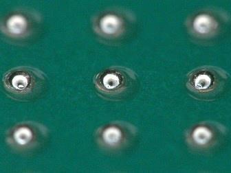
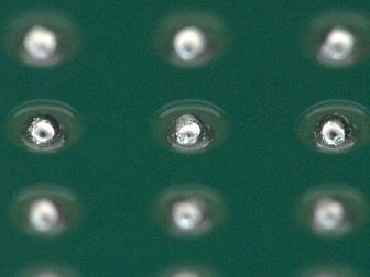
11 11 Head-in-Pillow Resistance Test method Test PCB: FR-4 Surface Finish: OSP Metal Stencil Thickness: 0.12mm (Laser) Test Pad Size: 0.8 x 0.8mm Loaded Balls: 0.76mm ball of SAC305 Heating Method: Solder bath at 275ºC Loading : 10sec. Pillow defect good NG Drop solder ball on molten solder every 10 seconds. Ball will not merge with solder paste when flux activation runs out. 30sec 40sec 60sec S3X58-M500-4 Conventional Product M500-4 behaves longer flux activation at higher temperatures maintaining high head-in-pillow resistance compared to conventional product.
12 12 Test method: BS EN14582 Measured Element Result F Not Detected Cl Not Detected Br Not Detected (ppm) M500-4 meets Halogen Free requirements (Br+Cl= below 1500ppm). Tested in accordance with BS EN14582.
13 13 Item Result Specification Tack Time > 48 hours JIS Z Slump Property 0.3mm, pass JIS Z Solder Ball < Category 3 JIS Z Copper Mirror Corrosion Type L IPC-TM Copper Plate Corrosion Pass IPC-TM SIR Test >1E+9 IPC-TM
14 14 1. Printing 1) Recommended Printing Condition (1) Squeegee 1. Shape : Flat 2. Material : Polyurethane or metal blade 3. Angle : 60º 4. Print Pressure : Relatively low 5. Print Speed : 20~100mm/sec. (2) Stencil 1. Thickness : 150~80 m when pitch is 0.65~0.4mm 2. Manufacturing Method : Laser or Additive 3. Stencil release speed : 7.0~10.0mm/sec. 4. Clearance : 0mm (3) Process Environment 1. Temperature : 23~27ºC 2. Humidity : 40~60%RH 3. Air Conditioning : Air draft in the printer dries up solder paste faster and deteriorates performance of the solder paste. Control the air flow by using a shield or other method. 2. Shelf Life 0~10ºC * How to interpret Lot Number ex. Lot No : 6 months after production date Batch #: 2 nd Batch Production Date: 27th Production Month: November Production Year: 2014

15 15 Recommended Reflow Profile (ºC) Pre-heat Temperature/ Duration 150~190ºC/ 60~100sec. Peak Temperature 230~250ºC 150 Duration above 219ºC: >30 sec Ramp-up Speed 1.0~3.0ºC/sec. Pre-heating Condition Recommended: 150~180ºC 90sec Upper Limit: 160~190ºC 100sec Lower Limit: 150~175ºC 60sec (sec.)


16 16 Supplement on Recommended Reflow Profile (ºC) Higher preheat temperature may accelerate oxidation of the solder powder and electrode, and degrade flux which results in grainy solder fillet and dewetting. In case of poor solder meltability, lower the preheat temperature Low peak temperature or short time above liquidus temperature inhibits void release. In case of high void ratio, raise peak temperature or extend time above liquidus temperature (>45 seconds). Slow temperature elevation between preheating to melt point may accelerate oxidation of the solder powder and electrode, and degrade flux which results in grainy solder fillet and dewetting. In case of poor solder meltability, increase the temperature elevation speed Fast ramp-up speed may cause birding or solder balling due to the heat slump. To improve bridging or solder balling, alleviate the ramp-up speed (sec.) (sec.)
& Anti-pillow. Product information. Koki no-clean LEAD FREE solder paste. Contents. Lead free SOLUTIONS you can TRUST.
 www.ko-ki.co.jp #46019E Revised on JUN 15, 2009 Koki no-clean LEAD FREE solder paste Super Low-Void & Anti-pillow Product information Pillow defect This Product Information contains product performance
M series. Product information. Koki no-clean LEAD FREE solder paste. Contents. Lead free SOLUTIONS you can TRUST.
 www.ko-ki.co.jp Ver. 42017e.2 Prepared on Oct. 26, 2007 Koki no-clean LEAD FREE solder paste Anti-Pillow Defect Product information This Product Information contains product performance assessed strictly
GSP. TOYOTA s recommended solder paste for automotive electronics. Product information. LEAD FREE solder paste.
 www.ko-ki.co.jp #47012E 2011.09.27 LEAD FREE solder paste TOYOTA s recommended solder paste for automotive electronics Product information Crack-Free Residue This Product Information contains product performance
TECHNICAL INFORMATION
 TECHNICAL INFORMATION Super Low Void Solder Paste SE/SS/SSA48-M956-2 [ Contents ] 1. FEATURES...2 2. SPECIFICATIONS...2 3. VISCOSITY VARIATION IN CONTINUAL PRINTING...3 4. PRINTABILITY..............4 5.
JU-48P. Heat Curable SMT Adhesive for Printing. Product Information. Heat Curing Type SMT Adhesive for Printing. Contents.
 www.ko-ki.co.jp #51010E Revised on June 16, 2014 Heat Curing Type SMT Adhesive for Printing Heat Curable SMT Adhesive for Printing JU-48P Product Information This Product Information contains product performances
Engineering Manual LOCTITE GC 10 T3 Solder Paste
 Engineering Manual LOCTITE GC T Solder Paste Suitable for use with: Standard SAC Alloys GC The Game Changer Contents. Performance Summary. Introduction: Properties, Features & Benefits. Operating Parameters
no-clean and halide free INTERFLUX Electronics N.V.
 Delphine series no-clean and halide free s o l d e r p a s t e INTERFLUX Electronics N.V. Product manual Key properties - Anti hidden pillow defect - Low voiding chemistry - High stability - High moisture
PRODUCT PROFILE ELECTROLOY NO CLEAN LEAD FREE PASTE
 PRODUCT PROFILE ELECTROLOY NO CLEAN LEAD FREE PASTE Product Name Product Code #515 LEAD FREE PASTE Sn99.0/Ag0.3/Cu0.7 EMCO#515-315P DOC CATEGORY: 3 PF EMCO#515-315P 14062010 REV.B Page 1 of 5 PRODUCT DESCRIPTION
Contact Material Division Business Unit Assembly Materials
 Contact Material Division Business Unit Assembly Materials MICROBOND SOP 91121 P SAC305-89 M3 C Seite 1 Print Performance Soldering Performance General Information MICROBOND SOP 91121 P SAC305-89 M3 Technical
Ultra-Low Voiding Halogen-Free No-Clean Lead-Free Solder Paste for Large Pads
 Ultra-Low Voiding Halogen-Free No-Clean Lead-Free Solder Paste for Large Pads Li Ma, Fen Chen, and Dr. Ning-Cheng Lee Indium Corporation Clinton, NY mma@indium.com; fchen@indium.com; nclee@indium.com Abstract
EF Solder Cream (V) (EFC-3C05)
 (EFC-3C05)") EF Solder Cream (V) (EFC3C05) www.ecojoin.co.kr EF Solder Cream Series Technical Data Sheet EFC3C05 (Sn3.0Ag0.5Cu) Ecojoin.co.,Ltd 7233, KorimDong, YongInSi, KyungKiDo,(449010), KOREA Http://www.ecojoin.co.kr
EF Solder Cream (V) (EFC3C05) www.ecojoin.co.kr EF Solder Cream Series Technical Data Sheet EFC3C05 (Sn3.0Ag0.5Cu) Ecojoin.co.,Ltd 7233, KorimDong, YongInSi, KyungKiDo,(449010), KOREA Http://www.ecojoin.co.kr
TECHNICAL INFORMATION S3X 60NH
 Lead free SOLUTIONS you can TRUST TECHNICAL INFORMATION Lead Free No-clean Flux Cored Solder Wire S3X 60NH 1. Features Excellent solderability offers good workability. Minimum flux spattering, easy separation
Bumping of Silicon Wafers using Enclosed Printhead
 Bumping of Silicon Wafers using Enclosed Printhead By James H. Adriance Universal Instruments Corp. SMT Laboratory By Mark A. Whitmore DEK Screen Printers Advanced Technologies Introduction The technology
Factbook Cobar OT2 Virtual
 Factbook OT2 Table of Contents 01 Table of contents 02 Handling guidelines OT2 solder paste 03 Printing continuous printing process window 04 Printing interval printing process window 05 Recommended reflow
Broadband Printing: The New SMT Challenge
 Broadband Printing: The New SMT Challenge Rita Mohanty & Vatsal Shah, Speedline Technologies, Franklin, MA Gary Nicholls, Ron Tripp, Cookson Electronic Assembly Materials Engineered Products, Johnson City,
SMT Troubleshooting. Typical SMT Problems For additional process solutions, please refer to the AIM website troubleshooting guide
 SMT Troubleshooting Typical SMT Problems For additional process solutions, please refer to the AIM website troubleshooting guide Solder Balling Solder Beading Bridging Opens Voiding Tombstoning Unmelted
Understanding the Effect of Process Changes and Flux Chemistry on Mid-Chip Solder Balling
 As originally published in the IPC APEX EXPO Conference Proceedings. Understanding the Effect of Process Changes and Flux Chemistry on Mid-Chip Solder Balling Katherine Wilkerson, Ian J. Wilding, Michael
Application Note AN-1011
 AN-1011 Board Mounting Application Note for 0.800mm Pitch Devices For part numbers IRF6100, IRF6100PBF, IR130CSP, IR130CSPPBF, IR140CSP, IR140CSPPBF, IR1H40CSP, IR1H40CSPPBF By Hazel Schofield and Philip
HKPCA Journal No. 10. Wetting of Fresh and Aged Immersion Tin and Silver Surface Finishes by Sn/Ag/Cu Solder. Minna Arra Flextronics Tampere, Finland
 Wetting of Fresh and Aged Immersion Tin and Silver Surface Finishes by Sn/Ag/Cu Solder Minna Arra Flextronics Tampere, Finland Dongkai Shangguan & DongJi Xie Flextronics San Jose, California, USA Abstract
Prepared by Qian Ouyang. March 2, 2013
 AN075 Rework Process for TQFN Packages Rework Process for TQFN Packages Prepared by Qian Ouyang March 2, 2013 AN075 Rev. 1.1 www.monolithicpower.com 1 ABSTRACT MPS proprietary Thin Quad Flat package No
HOW DOES PRINTED SOLDER PASTE VOLUME AFFECT SOLDER JOINT RELIABILITY?
 HOW DOES PRINTED SOLDER PASTE VOLUME AFFECT SOLDER JOINT RELIABILITY? ABSTRACT Printing of solder paste and stencil technology has been well studied and many papers have been presented on the topic. Very
SMART GROUP STANDARD. Control of Solder Paste used in Electronic Assembly Process. SMART Group. 2 Normative References
 2 Normative References The Test Methods employed are adapted from IPC-TM-650 comprising: SMART GROUP STANDARD Control of Solder Paste used in Electronic Assembly Process Number: SG PCT 01 Control of Solder
SMT Assembly Considerations for LGA Package
 SMT Assembly Considerations for LGA Package 1 Solder paste The screen printing quantity of solder paste is an key factor in producing high yield assemblies. Solder Paste Alloys: 63Sn/37Pb or 62Sn/36Pb/2Ag
A review of the challenges and development of. the electronics industry
 SMTA LA/OC Expo, Long Beach, CA, USA A review of the challenges and development of SMT Wave and Rework assembly processes in SMT, the electronics industry Jasbir Bath, Consulting Engineer Christopher Associates
The Impact of Reduced Solder Alloy Powder Size on Solder Paste Print Performance. Presented by Karl Seelig, V.P. Technology AIM Metals & Alloys
 The Impact of Reduced Solder Alloy Powder Size on Solder Paste Print Performance Presented by Karl Seelig, V.P. Technology AIM Metals & Alloys Solder Powder Solder Powder Manufacturing and Classification
TECHNICAL INFORMATION S03X7C-56M
 Lead free SOLUTIONS you can TRUST TECHNICAL INFORMATION Lead Free No-clean Flux Cored Solder Wire S03X7C-56M The alloy composition of the lead-free resin flux cored solder is now dominated by SnAg3.0Cu0.5,
Study on Solder Joint Reliability of Fine Pitch CSP
 As originally published in the IPC APEX EXPO Conference Proceedings. Study on Solder Joint Reliability of Fine Pitch CSP Yong (Hill) Liang, Hank Mao, YongGang Yan, Jindong (King) Lee. AEG, Flextronics
HOW DOES SURFACE FINISH AFFECT SOLDER PASTE PERFORMANCE?
 HOW DOES SURFACE FINISH AFFECT SOLDER PASTE PERFORMANCE? Tony Lentz FCT Assembly Greeley, CO, USA tlentz@fctassembly.com ABSTRACT The surface finishes commonly used on printed circuit boards (PCBs) have
TECHNICAL INFORMATION. S03X7Ca-56M
 Lead free SOLUTIONS you can TRUST TECHNICAL INFORMATION Lead Free No-clean Flux Cored Solder Wire The normal alloy composition of the lead free rosin flux cored solder wires, is now dominated by SnAg3.0Cu0.5
FILL THE VOID III. Tony Lentz FCT Assembly Greeley, CO, USA
 FILL THE VOID III Tony Lentz FCT Assembly Greeley, CO, USA tlentz@fctassembly.com ABSTRACT This study is part three in a series of papers on voiding in solder joints and methods for mitigation of voids.
Assembly Instructions for SCA6x0 and SCA10x0 series
 Technical Note 71 Assembly Instructions for SCA6x0 and SCA10x0 series TABLE OF CONTENTS Table of Contents...1 1 Objective...2 2 VTI'S DIL-8 and DIL-12 packages...2 3 Package Outline and Dimensions...2
Specification Table. Characteristics of J3-HFC-3 Test method
 Some features J3-HFC-32009.1 Halogen free type, Sn-Ag-Cu lead free flux cored wire solder Not adding any halogen, Chlorine (Cl) and Bromine (Br) Good solderability by not only hand soldering but also a
Application Note. Soldering Guidelines for Module PCB Mounting Rev 13
 Application Note Soldering Guidelines for Module PCB Mounting Rev 13 OBJECTIVE The objective of this application note is to provide ANADIGICS customers general guidelines for PCB second level interconnect
V349 (CLF5043) Halide Free No Clean Core Wire Fine Wire Applications
 Halide Free No Clean Core Wire Fine Wire Applications") Pb V349 (CLF5043) Halide Free No Clean Core Wire Fine Wire Applications INTRODUCTION Viromet* 349, with a composition of Sn/Ag/Cu/In + X, is one of the high-performance lead free solder available in the
Pb V349 (CLF5043) Halide Free No Clean Core Wire Fine Wire Applications INTRODUCTION Viromet* 349, with a composition of Sn/Ag/Cu/In + X, is one of the high-performance lead free solder available in the
Assembly Instructions for SCC1XX0 series
 Technical Note 82 Assembly Instructions for SCC1XX0 series TABLE OF CONTENTS Table of Contents...1 1 Objective...2 2 VTI's 32-lead Dual In-line Package (DIL-32)...2 3 DIL-32 Package Outline and Dimensions...2
Application Note 5026
 Surface Laminar Circuit (SLC) Ball Grid Array (BGA) Eutectic Surface Mount Assembly Application Note 5026 Introduction This document outlines the design and assembly guidelines for surface laminar circuitry
AN5046 Application note
 Application note Printed circuit board assembly recommendations for STMicroelectronics PowerFLAT packages Introduction The PowerFLAT package (5x6) was created to allow a larger die to fit in a standard
An Investigation into Lead-Free Low Silver Cored Solder Wire for Electronics Manufacturing Applications
 An Investigation into Lead-Free Low Silver Cored Solder Wire for Electronics Manufacturing Applications Shantanu Joshi 1, Jasbir Bath 1, Kimiaki Mori 2, Kazuhiro Yukikata 2, Roberto Garcia 1, Takeshi Shirai
Assembly Guidelines Sterling Silver & MacStan Immersion Tin Coated PCB s
 Assembly Guidelines Sterling Silver & MacStan Immersion Tin Coated PCB s By: MacDermind Final Finish Team MacDermid Inc. Flat solderable surface finishes are required for the increasingly dense PCB designs.
SOLDER PASTE PRINTING (DVD-34C) v.2
 v.2") This test consists of twenty multiple-choice questions. All questions are from the video: Solder Paste Printing (DVD-34C). Each question has only one most correct answer. Circle the letter corresponding
This test consists of twenty multiple-choice questions. All questions are from the video: Solder Paste Printing (DVD-34C). Each question has only one most correct answer. Circle the letter corresponding
Improve SMT Assembly Yields Using Root Cause Analysis in Stencil Design
 Improve SMT Assembly Yields Using Root Cause Analysis in Stencil Design Greg Smith FCT Assembly, Inc. Greeley, CO Abstract Reduction of first pass defects in the SMT assembly process minimizes cost, assembly
A FEASIBILITY STUDY OF CHIP COMPONENTS IN A LEAD-FREE SYSTEM
 A FEASIBILITY STUDY OF 01005 CHIP COMPONENTS IN A LEAD-FREE SYSTEM Chrys Shea Dr. Leszek Hozer Cookson Electronics Assembly Materials Jersey City, New Jersey, USA Hitoshi Kida Mutsuharu Tsunoda Cookson
Introduction of IMS Technology for Advanced Solder Bumping on Wafers / Laminates
 Introduction of IMS Technology for Advanced Solder Bumping on Wafers / Laminates Science & Technology IBM Research Tokyo Yasumitsu Orii, PhD Senju Metal Industry Co.,TW Deputy General Manager Lewis Huang
FPC CONNECTORS Y3FT (0.3 mm pitch) with FPC tabs
 with FPC tabs") AYF31 FPC CONNECTORS FOR FPC CONNECTION FPC CONNECTORS Y3FT (0.3 mm pitch) with FPC tabs (Former Name: YF31) FEATURES 1. Low-profile, space-saving design (pitch: 0.3mm) The 0.9mm height, 3.0mm depth contributes
AYF31 FPC CONNECTORS FOR FPC CONNECTION FPC CONNECTORS Y3FT (0.3 mm pitch) with FPC tabs (Former Name: YF31) FEATURES 1. Low-profile, space-saving design (pitch: 0.3mm) The 0.9mm height, 3.0mm depth contributes
BGA (Ball Grid Array)
") BGA (Ball Grid Array) National Semiconductor Application Note 1126 November 2002 Table of Contents Introduction... 2 Package Overview... 3 PBGA (PLASTIC BGA) CONSTRUCTION... 3 TE-PBGA (THERMALLY ENHANCED
BGA (Ball Grid Array) National Semiconductor Application Note 1126 November 2002 Table of Contents Introduction... 2 Package Overview... 3 PBGA (PLASTIC BGA) CONSTRUCTION... 3 TE-PBGA (THERMALLY ENHANCED
A. Special feature. B. Basic characteristic J3-ESM
 A. Special feature 1. Solderability test for nickel 2. Solderability test for stainless 3. Reliability of J3-ESM-3 3-1: Insulation resistance test 3-2: Humidity test under DC voltage (Migration test) 4.
VT-35 SOLDER PASTE PRINTING DEFECT ANALYSIS AND PREVENTION. Script Writer: Joel Kimmel, IPC
 VIDEO VT-35 SOLDER PASTE PRINTING DEFECT ANALYSIS AND PREVENTION Script Writer: Joel Kimmel, IPC Below is a copy of the narration for the VT-35 videotape. The contents for this script were developed by
Grypper GrypperG40 GrypperG80
 Grypper GrypperG40 GrypperG80 High performance net zero footprint engineering test sockets ATTACHMENT AND REMOVAL GUIDE Before You Begin ABOUT THIS GUIDE Welcome to the Grypper Product Test Socket Attachment
Improve SMT Assembly Yields Using Root Cause Analysis in Stencil Design
 Improve SMT Assembly Yields Using Root Cause Analysis in Stencil Design Greg Smith FCT Assembly, Inc. gsmith@fctassembly.com This paper and presentation was first presented at the 2017 IPC Apex Expo Technical
Process Parameters Optimization For Mass Reflow Of 0201 Components
 Process Parameters Optimization For Mass Reflow Of 0201 Components Abstract The research summarized in this paper will help to address some of the issues associated with solder paste mass reflow assembly
Meeting Future Stencil Printing Challenges with Ultrafine Powder Solder Pastes
 Meeting Future Stencil Printing Challenges with Ultrafine Powder Solder Pastes Authored by: Ed Briggs, Indium Corporation Abstract The explosive growth of personal electronic devices, such as mobile phones,
SMTA Great Lakes Chapter Meeting
 SMTA Great Lakes Chapter Meeting IPC-7711B/7721B Rework, Repair and Modification Presented By: Frank Honyotski Master IPC Trainer (MIT) STI Electronics, Inc. 1.1 Scope Procedure for rework/repair Aggregate
Practical Solutions for Successful Pb-Free Soldering. Brian Allder Qualitek-Europe
 Practical Solutions for Successful Pb-Free Soldering Brian Allder Qualitek-Europe Challenges/Barriers to Lead Free Cost Material Availability Process Modifications Material Compatibility Standards Inspection
HOTBAR REFLOW SOLDERING
 HOTBAR REFLOW SOLDERING Content 1. Hotbar Reflow Soldering Introduction 2. Application Types 3. Process Descriptions > Flex to PCB > Wire to PCB 4. Design Guidelines 5. Equipment 6. Troubleshooting Guide
An Introduction to Electronics Systems Packaging. Prof. G. V. Mahesh. Department of Electronic Systems Engineering
 An Introduction to Electronics Systems Packaging Prof. G. V. Mahesh Department of Electronic Systems Engineering Indian Institute of Science, Bangalore Module No. # 07 Lecture No. # 33 Reflow and Wave
Ultra Fine Pitch Printing of 0201m Components. Jens Katschke, Solutions Marketing Manager
 Ultra Fine Pitch Printing of 0201m Components Jens Katschke, Solutions Marketing Manager Agenda Challenges in miniaturization 0201m SMT Assembly Component size and appearance Component trends & cooperation
Selective Soldering for Interconnection Technology Used in Enterprise Communication Apparatuses
 Selective Soldering for Interconnection Technology Used in Enterprise Communication Apparatuses Mark Woolley, Wesley Brown, and Dr. Jae Choi Avaya Inc. 1300 W 120 th Avenue Westminster, CO 80234 Abstract:
AND8081/D. Flip Chip CSP Packages APPLICATION NOTE
 Flip Chip CSP Packages Prepared by: Denise Thienpont ON Semiconductor Staff Engineer APPLICATION NOTE Introduction to Chip Scale Packaging This application note provides guidelines for the use of Chip
Module No. # 07 Lecture No. # 35 Vapour phase soldering BGA soldering and De-soldering Repair SMT failures
 An Introduction to Electronics Systems Packaging Prof. G. V. Mahesh Department of Electronic Systems Engineering Indian Institute of Science, Bangalore Module No. # 07 Lecture No. # 35 Vapour phase soldering
A COMPARATIVE STUDY OF BALL GRID ARRAY AND ULTRA FINE-PITCH QFP TECHNOLOGIES USING SOLDER PASTE STENCIL PRINTING
 A COMPARATIVE STUDY OF BALL GRID ARRAY AND ULTRA FINE-PITCH QFP TECHNOLOGIES USING SOLDER PASTE STENCIL PRINTING Roger Rörgren, Per Carlsson and Johan Liu IVF - The Swedish Institute of Production Engineering
J O I N T I N D U S T R Y S T A N D A R D. Requirements for Soldering Pastes J Standard 005A. December 2011
 J O I N T I N D U S T R Y S T A N D A R D Requirements for Soldering Pastes J Standard 005A December 2011 Requirements for Soldering Pastes 1.0 SCOPE 1.1 Scope This standard prescribes general requirements
WLP User's Guide. CMOS IC Application Note. Rev.1.0_03. ABLIC Inc., 2014
 CMOS IC Application Note WLP User's Guide ABLIC Inc., 2014 This document is a reference manual that describes the handling of the mounting of super-small WLP (Wafer Level Package) for users in the semiconductor
Technical Note 1 Recommended Soldering Techniques
 1 Recommended Soldering Techniques Introduction The soldering process is the means by which electronic components are mechanically and electrically connected into the circuit assembly. Adhering to good
Ceramic Monoblock Surface Mount Considerations
 Introduction Technical Brief AN1016 Ceramic Monoblock Surface Mount Considerations CTS ceramic block filters, like many others in the industry, use a fired-on thick film silver (Ag) metallization. The
Investigating the Component Assembly Process Requirements
 Investigating the 01005-Component Assembly Process Requirements Rita Mohanty, Vatsal Shah, Arun Ramasubramani, Speedline Technologies, Franklin, MA Ron Lasky, Tim Jensen, Indium Corp, Utica, NY Abstract
Understanding stencil requirements for a lead-free mass imaging process
 Electronics Technical Understanding stencil requirements for a lead-free mass imaging process by Clive Ashmore, DEK Printing Machines, United Kingdom Many words have been written about the impending lead-free
LED Mounting Techniques
 LED Mounting Techniques Contents 1. Introduction 2. Solder Paste Printing 3. LED Placement 4. Reflow Soldering 5. Verification of LED Mounting Performance 6. Others 7. Request 1/13 LED Mounting Techniques
A Technique for Improving the Yields of Fine Feature Prints
 A Technique for Improving the Yields of Fine Feature Prints Dr. Gerald Pham-Van-Diep and Frank Andres Cookson Electronics Equipment 16 Forge Park Franklin, MA 02038 Abstract A technique that enhances the
Improve SMT Assembly Yields Using Root Cause Analysis in Stencil Design
 Improve SMT Assembly Yields Using Root Cause Analysis in Stencil Design Greg Smith FCT Assembly, Inc. gsmith@fctassembly.com This paper and presentation was first presented at the 2017 IPC Apex Expo Technical
BREAKING THROUGH FLUX RESIDUES TO PROVIDE RELIABLE PROBING ON PCBAS- CONSISTENT CONNECTIONS ACROSS DIFFERENT NO-CLEAN SOLDERS, FLUXES AND LAND DESIGNS
 BREAKING THROUGH FLUX RESIDUES TO PROVIDE RELIABLE PROBING ON PCBAS- CONSISTENT CONNECTIONS ACROSS DIFFERENT NO-CLEAN SOLDERS, FLUXES AND LAND DESIGNS Paul Groome, Ehab Guirguis Digitaltest, Inc. Concord,
AN-5067 PCB Land Pattern Design and Surface Mount Guidelines for MLP Packages
 Introduction AN-5067 Fairchild Semiconductor Application Note September 2005 Revised September 2005 PCB Land Pattern Design and Surface Mount Guidelines for MLP Packages The current miniaturization trend
Is Now Part of To learn more about ON Semiconductor, please visit our website at
 Is Now Part of To learn more about ON Semiconductor, please visit our website at www.onsemi.com ON Semiconductor and the ON Semiconductor logo are trademarks of Semiconductor Components Industries, LLC
Fill the Void IV: Elimination of Inter-Via Voiding
 Fill the Void IV: Elimination of Inter-Via Voiding Tony Lentz FCT Assembly Greeley, CO, USA Greg Smith BlueRing Stencils Lumberton, NJ, USA ABSTRACT Voids are a plague to our electronics and must be eliminated!
Stencil Printing of Small Apertures
 Stencil Printing of Small Apertures William E. Coleman Ph.D. Photo Stencil, Colorado Springs, CO Abstract Many of the latest SMT assemblies for hand held devices like cell phones present a challenge to
Application Specification Slim WtoB Poke-in Connector
 Application Specification 114-137049 Slim WtoB Poke-in Connector 18APR 2016 REV:B 1. INTRODUCTION This specification covers the requirements for application of Slim WtoB Poke in connector for use on lighting
Is Now Part of To learn more about ON Semiconductor, please visit our website at
 Is Now Part of To learn more about ON Semiconductor, please visit our website at www.onsemi.com ON Semiconductor and the ON Semiconductor logo are trademarks of Semiconductor Components Industries, LLC
Solder Pastes. for electronics manufacturing. Solder Wires Solder Pastes Fluxes Solder Bars
 Solder Wires Solder Pastes Fluxes Solder Bars Soldering equipment Measurement and testing systems Conformal Coatings Accessories Solder Pastes for electronics manufacturing WE HAVE THE RIGHT SOLDER PASTE
BOARD DESIGN, SURFACE MOUNT ASSEMBLY AND BOARD LEVEL RELIABILITY ASPECTS OF FUSIONQUAD TM PACKAGES
 BOARD DESIGN, SURFACE MOUNT ASSEMBLY AND BOARD LEVEL RELIABILITY ASPECTS OF FUSIONQUAD TM PACKAGES Ahmer Syed 1, Sundar Sethuraman 2, WonJoon Kang 1, Gary Hamming 1, YeonHo Choi 1 1 Amkor Technology, Inc.
ECMF2-0730V12M12. Common mode filter with ESD protection for USB2.0 interface. Applications. Description. Features. Complies with following standards
 Common mode filter with ESD protection for USB2.0 interface Datasheet - production data V BUS high power TVS diode: V RM = 13.2 V I PP (8/20 µs): 70 A Very low PCB space consumption Thin package: 0.55
APPLICATION NOTE 6381 ORGANIC LAND GRID ARRAY (OLGA) AND ITS APPLICATIONS
 AND ITS APPLICATIONS") Keywords: OLGA, SMT, PCB design APPLICATION NOTE 6381 ORGANIC LAND GRID ARRAY (OLGA) AND ITS APPLICATIONS Abstract: This application note discusses Maxim Integrated s OLGA and provides the PCB design and
Keywords: OLGA, SMT, PCB design APPLICATION NOTE 6381 ORGANIC LAND GRID ARRAY (OLGA) AND ITS APPLICATIONS Abstract: This application note discusses Maxim Integrated s OLGA and provides the PCB design and
Application Specification Releasable Poke-in Connector 08JUL 2015 REV:A
 Application Specification 114-137055 Releasable Poke-in Connector 08JUL 2015 REV:A 1. INTRODUCTION This specification covers the requirements for application of Releasable Poke-in connector for use on
STENCIL CONSIDERATIONS FOR MINIATURE COMPONENTS
 STENCIL CONSIDERATIONS FOR MINIATURE COMPONENTS William E. Coleman, Ph.D. Photo Stencil Colorado Springs, CO, USA ABSTRACT SMT Assembly is going through a challenging phase with the introduction of miniature
DOES PCB PAD FINISH AFFECT VOIDING LEVELS IN LEAD-FREE ASSEMBLIES?
 DOES PCB PAD FINISH AFFECT VOIDING LEVELS IN LEAD-FREE ASSEMBLIES? David Bernard Dage Precision Industries Fremont, CA d.bernard@dage-group.com Keith Bryant Dage Precision Industries Aylesbury, Buckinghamshire,
For board-to-fpc. Narrow pitch connectors (0.4mm pitch)
") Automation Controls Catalog For board-to-fpc Narrow pitch connectors (0.4mm pitch) F4 Series 5.0mm 4.1mm RoHS compliant FEATURES 1. 0.9 mm mated height low profile two-piece type connectors 2. Strong resistance
Automation Controls Catalog For board-to-fpc Narrow pitch connectors (0.4mm pitch) F4 Series 5.0mm 4.1mm RoHS compliant FEATURES 1. 0.9 mm mated height low profile two-piece type connectors 2. Strong resistance
WB/WT/WXSC 250µm/WLSC100µm - Assembly by Wirebonding
 General description This document describes the attachment techniques recommended by Murata* for their vertical capacitors on the customer substrates. This document is non-exhaustive. Customers with specific
'*+,+$&#' ' '") !"#$%&'()'*"+,+$&#' *";
!"#$%&'()'*"+,+$&#' *"; Assembling SRD Products Onto Customer s PWBs. murata.com Copyright Murata Manufacturing Co., Ltd. All rights reserved.
 Assembling SRD Products Onto Customer s PWBs 1 24 February 2017 1 murata.com Assembling SRD Products Onto Customer s PWBs Considerations/Topics PWB footprint (layout) Solder mask use/layout Type of solder
Performance Enhancing Nano Coatings: Changing the Rules of Stencil Design. Tony Lentz
 Performance Enhancing Nano Coatings: Changing the Rules of Stencil Design Tony Lentz tlentz@fctassembly.com Outline/Agenda Introduction Experimental Design Results of Experiment Conclusions Acknowledgements
Application Note 5334
 Soldering and Handling of High Brightness, Through Hole LED Lamps Application Note 5334 Introduction LEDs are well known for their long useful life compared to conventional incandescent bulb. If an LED
Murata Silicon Capacitors WBSC / WTSC / WXSC 250 µm / WLSC 100 µm Assembly by Wirebonding. Table of Contents
 Table of Contents Table of Contents...1 Introduction...2 Handling Precautions and Storage...2 Pad Finishing...2 Process Flow with Glue...2 Process Flow with Solder Paste...3 Recommendations concerning
Print Performance Studies Comparing Electroform and Laser-Cut Stencils
 Print Performance Studies Comparing Electroform and Laser-Cut Stencils Rachel Miller Short William E. Coleman Ph.D. Photo Stencil Colorado Springs, CO Joseph Perault Parmi Marlborough, MA ABSTRACT There
Transistor Installation Instructions
 INTRODUCTION When inserting high power RF transistor packages into amplifier circuits there are two important objectives. Firstly, removing heat and, secondly, providing a longterm reliable solder joint
Automotive Devices: Quad No- Lead (QFN) Technology with Inspectable Solder Connections
 Technology with Inspectable Solder Connections") Automotive Devices: Quad No- Lead (QFN) Technology with Inspectable Solder Connections FTF-SDS-F0026 Dwight Daniels Package Engineer A P R. 2 0 1 4 TM External Use Agenda Wettable Lead Ends / Definition
Automotive Devices: Quad No- Lead (QFN) Technology with Inspectable Solder Connections FTF-SDS-F0026 Dwight Daniels Package Engineer A P R. 2 0 1 4 TM External Use Agenda Wettable Lead Ends / Definition
Version: 1.2 Document code:ma2512 Effective date : Page: 1 of 7. Metal Alloy shunt resistor MA2512 series ROHS
 Document code: Page: 1 of 7 Metal Alloy shunt resistor series ROHS Metal Alloy Shunt Resistor Specification Document code: Page: 2 of 7 Metal Alloy shunt resistor series ROHS Scope This specification applies
TVNow TM (FR01-B1-S-0-047) Mobile TV Dual-band DVB-H
 Mobile TV Dual-band DVB-H") Mobile TV Dual-band DVB-H (UHF + L band) Antenna Fractus Antennas specializes in enabling effective mobile communications. Using Fractus technology, we design and manufacture optimized antennas to make
Mobile TV Dual-band DVB-H (UHF + L band) Antenna Fractus Antennas specializes in enabling effective mobile communications. Using Fractus technology, we design and manufacture optimized antennas to make
RHEOLOGY AND WETTING CHARACTERIZATIONS OF FLUX AND SOLDER PASTE FOR BGA PACKAGES
 s originally published in the SMT Proceedings RHEOLOGY ND WETTING HRTERIZTIONS OF FLUX ND SOLDER PSTE FOR G PKGES Jinlin Wang, Ph.D. Intel orporation handler, Z, US Jinlin.wang@intel.com STRT Package failures
In data sheets and application notes which still contain NXP or Philips Semiconductors references, use the references to Nexperia, as shown below.
 Important notice Dear Customer, On 7 February 2017 the former NXP Standard Product business became a new company with the tradename Nexperia. Nexperia is an industry leading supplier of Discrete, Logic
NPL Report MATC(A)18 The Effect of Solder Alloy, Metal Particle Size and Substrate Resist on Fine Pitch Stencil Printing Performance
18 The Effect of Solder Alloy, Metal Particle Size and Substrate Resist on Fine Pitch Stencil Printing Performance") NPL Report The Effect of Solder Alloy, Metal Particle Size and Substrate Resist on Fine Pitch Stencil Printing Performance Ling Zou, Milos Dusek, Martin Wickham & Christopher Hunt August 01 NPL Report
NPL Report The Effect of Solder Alloy, Metal Particle Size and Substrate Resist on Fine Pitch Stencil Printing Performance Ling Zou, Milos Dusek, Martin Wickham & Christopher Hunt August 01 NPL Report
JOINT INDUSTRY STANDARD. Requirements for Soldering Pastes J Standard 005A. June 2011 Final Draft for Industry Comment
 JOINT INDUSTRY STANDARD Requirements for Soldering Pastes J Standard 005A Requirements for Soldering Pastes Amendment 1 1.0 SCOPE 1.1 Scope This standard prescribes general requirements for the characterization
Initial release of document
 This specification covers the requirements for application of SMT Poke In Connectors for use on printed circuit (pc) board based LED strip lighting typically used for sign lighting. The connector accommodates