A review of the challenges and development of. the electronics industry
|
|
|
- Byron Ramsey
- 5 years ago
- Views:
Transcription
1 SMTA LA/OC Expo, Long Beach, CA, USA A review of the challenges and development of SMT Wave and Rework assembly processes in SMT, the electronics industry Jasbir Bath, Consulting Engineer Christopher Associates Inc./ Koki Solder Jasbir@christopherweb.com www christopherweb com Lead Free SOLUTIONS you can TRUST Challenging New Technologies
2 Agenda Introduction SMT Wave Rework Test Conclusions Future Work
3 Introduction 3 The electronics assembly industry has been migrating from PTH to SMT over a number of years. This migration has seen a number of new components and technologies faced by the industry. The presentation will review the various new components and assembly challenges faced.
4 SMT Component Trends Move to miniaturization and System In Package type components Large System in Package components QFN/MLF/BTC components CSP/BGA components Chip components
 Modules Large BGAs/SIP sizes: 35mm to 55mm PoP 3000 to 3500 I/O with 0.")
5 Large System in Package components Increase in use of System in Package (SIP) components: Stacked Die in Package Stacked Package on Package (PoP) Modules Large BGAs/SIP sizes: 35mm to 55mm PoP 3000 to 3500 I/O with 0.8mm to 1mm pitch
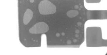
6 Issues with large component sizes (SiP, PoP) Solder paste printing issues Component placement issues Coplanarity issues of component and board during assembly Potential for warpage of part during reflow (Head-in-Pillow defect) Issues during area array rework (high component temperatures, warpage during rework)

7 Warpage related to PoP assembly 7 Component warpage during the reflow process can lead to solder joint opens. More problematic with PoP components where each package is made thinner to minimize overall height, making it more vulnerable to warpage. Once solder bumps of PoP component separate from board pad land, even if they are in contact again, open solder joint failures result due to depleted tacky flux performance during reflow. Ref: J. Bath et. al, (Christopher/Koki) SMTAI Conference, 2010.
8 Reflow Issues Related to Package on Package (PoP) Components Work needed to improve assembly yields: warpage of the part during reflow Tacky flux versus Low viscosity solder paste for package attachment during reflow Tacky flux: Would the solder joint reliability be acceptable and potential for warpage Solder paste: Would solder bridging be an issue during assembly
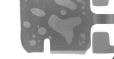
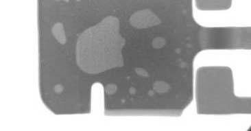
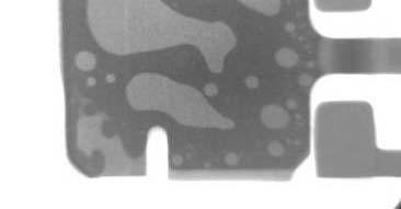
9 Affect on Powder Size on solder paste transfer for PoP components Tests with Type 4 (20-38um) solder powder size versus 10-25um versus 5-20um for PoP showed the best results with 5-20um in terms of good paste transfer. Good paste amount deposited helped reduce head-in-pillow component soldering issues. 9 Ref: J. Bath et. al, (Christopher/Koki), SMTAI Conference, 2010.
10 Issues Related to Assembly of QFN/MLF/BTC (Micro Lead-Frame) Components Non-standard designs from component suppliers Refer to IPC 7093 standard for general guidelines: Design and Assembly Guidelines for BTC/MLF/QFN components Need to optimize solder paste volumes to use: Large center pad (voiding) Center Pad Via Plugging: Optimize i to reduce Voiding Soldering to edge of QFN/MLF which would have oxidized copper: decide on need to rework Low QFN/MLF standoff height (flux entrapment/ unactivated flux) Inspection difficulties for multiple rows of this component type
11 Issues Related to Rework of QFN/MLF/BTC (Micro- Lead-Frame) Components Potential high temperature component related issues Not very well standardized rework techniques (area array, hand soldering) Decide on use of solder paste or tacky flux during QFN rework and dhow to apply it.
12 QFN/BTC/MLF Reflow problems (Voiding) Develop suitable solder paste reflow profile to reduce voiding Assessment of solder paste to use. Solderability/ void exit issues under QFN/MLF component Voiding categories: Greater than 25% voiding termed a defect (IPC 610 standard) At what % over 25% will there be ATC or mechanical reliability issues. Potential void issues in terms of electrical/ thermal requirements for QFN/MLF what void % is an issue


13 Development of solder paste helps to reduce voiding in QFN/BTC/MLF. Tests on different board surface finishes on power transistor component showing different levels of voiding %. 13 Improved Lead-free Paste C OSP Sn NiAu HASL (SAC305) 2.55% 3.6% 5.4% 4.6% Conventional Lead-free Paste D OSP Sn NiAu HASL (SAC305) 25.2% 35.0% 17.5% 17.4% Ref: J.Bath et al. (Christopher Associates/ Koki Solder) SMTAI 2010
14 Development of solder paste to reduce voiding under QFN/MLF/BTC component 14 Improved wetting property for Lead-free Paste C extends duration of fluid/active state of the flux: Model: behav ior of v oids during reflow process Helps to push out more of the entrapped gas Remov al of oxidized f ilm & f low of flux prompt bubbles to ev acuate. Enables component to come closer to board pad, lowering component solder joint standoff height. New additiv e with good wetting properties pulls the component and helps to push out the bubbles. REF: J.Bath et al. (Christopher Associates. Koki solder) SMTAI 2010
15 Assembly with CSP/WL-CSP Components Reduction in CSP pitch: From 0.5mm to 0.4mm to 0.3mm Need to understand reliability implications for low volume solder joints such as 0.3mm pitch CSP Low profile CSP part (Potential flux activation issues) Solder Joint Voiding Warpage of part (Head in Pillow defect) Solder paste volume deposited and solder powder size used (Type 4 or 5 particle size paste for 0.3mm CSP versus Type 3 paste for coarser pitch components) Board Pad and Stencil design guideline recommendations
16 Assembly of Chip Components From 0402 to 0201 to chip components Board pad design considerations Stencil design (stencil thickness and aperture) Paste volume deposited and solder paste powder size used (Type 4 or 5 powder size paste for chip components) Placement accuracy of chip components Offset component placement in certain equipment dependent on paste location to board pad location Reflow behaviour Reworkability More challenges as movement is made from 0402 to 0201 to 01005
17 Board Pad and Stencil Design Guidelines for existing and emerging components Board Pad Design First step to optimize: Pad designs based on IPC design standards d (IPC 7351) or OEM/EMS guideline Understand how board pad designs were developed: Were they based on company evaluations or manufacturing yield data. Stencil aperture design Dependant on board pad designs and components used Refer to IPC stencil standards (IPC 7525) or OEM/EMS guidelines Understand how stencil aperture designs were developed Understand d stencil area ratios and aspect ratios for effective solder paste printing
18 SMT Solder Paste Printing As component sizes become smaller with smaller pad sizes, stencil area ratios guidelines are being challenged (Printing challenges when area ratios are < 0.66 and aspect ratios < 1.5). For a mix of large and small components on same board, more challenge to print large & small paste deposits on the board. 18 Courtesy: DEK Printing Machines


19 SMT Printing 19 Other solutions are being developed such as DEK Active Squeegee to print solder paste on a board with a mix of coarse and very fine pitch components (01005, 0.3mm CSP) [e.g. mobile phone type applications). Courtesy: DEK Printing Machines
20 Paste Inspection Equipment As more focus is placed on printing large and small paste deposits on same board in addition to ensuring printing accuracy and deposition, more use of paste inspection equipment. Use of 2D or 3D paste inspection increasing (move towards 3D paste inspection). Used for prototype builds and manufacturing. More emphasis needed on use of paste inspection not just to filter out some low solder paste print deposited boards but as a way to improve process yield.
21 Use of AOI (Automated Optical Inspection) and X-ray equipment AOI equipment considerations: AOI use after component placement (for high volume production) AOI use after reflow (for initial Prototype/NPI) X-ray equipment applications: Voiding detection in BGA/CSP and QFN/MLF/BTC components Holefill analysis for wave soldered TH components
22 Trend for Increased SMT Usage vs Wave Soldering with Paste-in-hole soldering More paste in hole processes mainly for consumer type products where board thickness is less than 63mil Greater than 63 mils more paste needed for good holefill with use of solder preforms but process window becomes more challenging to get good holefill Need to ensure paste in hole reflow soldered components are higher temperature rated for reflow versus wave soldering Need to ensure paste in hole soldered components can be reworked at lead-free reflow soldering temperatures Developments ongoing indicating that Paste in Hole can be used for thicker boards for assembly and rework [Ref: G.Subbarayan et. al: IPC APEX 2011, SMTAI 2011]
23 Lead-free SMT Alloys and Reflow Profiles used SMT solder pastes: Mainly Sn3-4Ag0.5Cu Some Sn1Ag0.5Cu and Sn0.7Cu based alloys Reflow Profiles: Tin-Lead: Time over 183ºC: sec, Peak: ºC Lead-free (Sn3-4Ag0.5Cu): Time over 217ºC: sec, Peak: ºC Lead-free Low silver alloys (Sn0.3Ag0.7Cu): Time over 227ºC: 30-90sec, Peak: 240C-270ºC
24 Issues transitioning to Low Silver Alloys for SMT Higher melting temperature SnAgCu alloys Sn3-4Ag0.5Cu (MP: 217ºC) Sn1Ag0.5Cu (MP:225ºC) to Sn0.7Cu (MP: 227ºC) Increased soldering temperatures, more likelihood of component and boardtemperature issues Need for updated component rating standards for Low Ag solder pastes [IPC/JEDEC J STD 020 standard] d]
25 Current Lead-free Alloys used and Issues Transitioning to Low Ag alloys for Wave Wave Alloys: Sn3-4Ag0.5Cu and Sn0.7Cu based alloys Increased solder usage in Wave machines versus SMT with more SnCu based lead-free wave alloys used due to cost Sn0.7CuNi, Sn0.7CuAg and Sn0.7CuAgNi (JEITA) alloys Lower Ag amount, lower cost: MP 227ºC vs Sn3-4Ag0.5Cu MP 217ºC JEITA alloys: Sn1Ag0.7Cu, Sn0.3Ag0.7Cu, Sn0.3Ag0.7Cu0.03Ni Sn0.7Cu based alloys Thicker boards: Higher pot temperatures- potential component and board issues and reduced wave holefill.
26 Wave Flux, Flux Spray Assessment and Wave Preheat Wave fluxes Trend to move to no-clean alcohol based wave fluxes for good holefill on thicker boards for lead-free Flux spray coverage assessment on board Flux Coverage/Board Penetration ti Assessment Good flux penetration Even spray pattern across surface assessed using flux paper Wave Board Preheat Important to consider amount of heat transfer into board Pre-heater: Pre-heater settings for optimized flux activation with more top-side preheat for better solder holefill

 Component types- Radial caps, LEDs,")
 270 C solder pot temperature with Sn3Ag0.5Cu solder Ref: S.")
27 Example of Lead-free Wave Soldering Evaluation DCC RJ-45, USB CAP CAP 125 mils (3.2mm) thick board 18 layers, 11 oz total copper OSP Board surface finish (High temperature rated) Component types- Radial caps, LEDs, RJ45, USB & DCC Board size- 16 inch x 11inch High Tg FR4 laminate (175 C) 270 C solder pot temperature with Sn3Ag0.5Cu solder Ref: S. Gopalkumar et al. (Brocade, Foxconn and BTC), SMTAI 2010
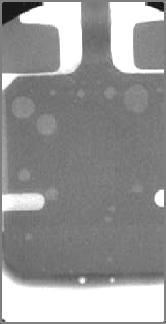
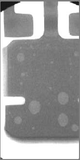
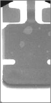
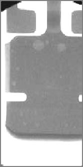
28 Flux Screening Evaluation Results- 2D X-ray 1 (Signal) 50%~75% 2 (GND) 25%~50% 1 (Signal) >75% 2 (GND) 25%~50% 1 (GND) >75% 2 (Signal) >75% 1 (Signal) 25%~50% 2 (Signal) 25%~50% C46 C126 CR6 CR15 1 (Signal) >75% 1 (No Connect) >75% 2 (No Connect) >75% 3 (Signal) >75% 4 (Signal) >75% 5 (Signal) >75% 6 (Signal) >75% 7 (No Connect) >75% 8 (no Connect) >75% 9 G >75% 10 G >75% 1 (Signal) >75% 2 (Signal) >75% 3 (Signal) >75% 4 (Signal) >75% 5 (Signal) >75% 6 (Signal) >75% 7 (Signal) >75% 8 (Signal) >75% 9 (Signal) >75% 10 (GND) >75% 11 G >75% 12 G >75% 13 (Signal) 0%~25% 14 (Signal) >75% 15 (Signal) >75% 16 (Signal) >75% 2 (Signal) >75% 3 (Signal) >75% 4 (Signal) >75% 5 (Signal) >75% 6 (Signal) >75% 7 (Signal) >75% 8 (Signal) >75% 9 (Signal) >75% 10 (GND) >75% 11 G 25%~50% 12 G >75% 13 (Signal) >75% 14 (Signal) >75% 15 (Signal) >75% 16 (Signal) >75% 1 (Signal) >75% 2 (Signal) >75% 3 (Signal) >75% 4 (GND) >75% 5 (No Connect) 50%~75% 6 (No Connect) 50%~75% J12 J25 J27 J39 1 (P48V_RTN) 50%~75% 2 (P48V_DCC_ON) >75% 3 (P48V_RTN) >75% 4 (GND) >75% 5 (P12V_CP) >75% 1 (GND) 50%~75% 2 (Signal) >75% 3 (Signal) >75% 1 (Signal) >75% 2 (GND) 50%~75% 3 (Signal) >75% 4 (Signal) >75% 4 (GND) 50%~75% U32_1 U32_2 U109 U181 Incomplete wave solder barrel fill across most components on the pins connected to ground planes Ref: S. Gopalkumar et al. (Brocade, Foxconn and BTC), SMTAI Brocade Communications Systems, Inc. CONFIDENTIAL For Internal Use Only 11/2/


,SMTAI 2010 2010")
29 Results of Lead-free Wave Process Optimization Flux optimization Board redesign Preheat optimization Improved holefill with combination of above factors especially board redesign Ref: S. Gopalkumar et al.(brocade, Foxconn and BTC),SMTAI Brocade Communications Systems, Inc. 11/2/


![5 mils [12 um]) 44 m 56 m DCC 40](/docs-images/82/85046659/images/30-3.jpg "m 39 m 40 m 50 m Ref: S.")
,SMTAI")
30 Lead-free Wave Soldering Confirmation Run Results Cross-section results showed good barrel fill with no significant copper dissolution (Cu thickness>0.5 mils [12 um]) 44 m 56 m DCC 40 m 39 m 40 m 50 m Ref: S. Gopalkumar et al.(brocade, Foxconn and BTC),SMTAI Brocade Communications Systems, Inc. CONFIDENTIAL 11/2/
31 Current Rework Alloys and Issues Transitioning to Low Ag Lead-free Rework Alloys Rework Alloys: Sn3-4Ag0.5Cu, Sn3.5Ag, Sn0.7Cu based alloys Hand soldering: Sn0.7Cu based alloys (lower cost) Potentially higher soldering iron tip temperatures especially for thicker more thermally demanding board BGA/CSP rework Sn0.7Cu based alloys (lower cost) Higher board and component temperatures Mini-pot/solder fountain: Good holefill/ low copper dissolution Sn0.7Cu+Ni Sn0.7Cu0.3Ag0.03Ni(JEITA alloy) Higher board and component temperatures
32 Rework Flux Trends Hand-soldering Tacky flux versus liquid flux versus cored wire General trend to cored wire or tacky flux Hand soldering heat activation questions with use of liquid flux and tacky flux BGA/CSP rework Solder paste (typically for larger BGA) or tacky flux (CSP) Mini-pot/ solder fountain Liquid flux or tacky flux
 thick board, 18 layers, 11 oz total copper OSP Board surface finish (High temperature")


33 Example of Lead-free Wave Rework Evaluation 125 mils (3.2mm) thick board, 18 layers, 11 oz total copper OSP Board surface finish (High temperature rated) Component types used for rework- RJ45, LED & DCC RJ45 connector and LED connector low/medium complexity DCC component high complexity Board size- 16 inch x 11inch, High Tg FR4 laminate (175ºC) 1 st pass wave soldering with Sn3Ag0.5Cu using wave pot temperature of 270ºC. Rework with Sn0.7Cu0.05Ni alloy with solder fountain pot temperature of 270ºC. Ref: S. Gopalkumar et al. (Brocade, Foxconn and BTC), SMTAI 2011
34 Effect of Reduced Preheat Temperature on Holefill during Lead-free PTH Rework Reduction of topside board temperature below 80ºC on DCC component resulted in reduced hole fill (40%) for component that did not meet IPC610 standard requirements. Ref: S. Gopalkumar et al. (Brocade, Foxconn and BTC), SMTAI


.")

35 DCC Component Lead-free Wave Rework Results with increased topside board preheat 35 X-ray image and cross-section of reworked DCC component showing good holefill (100%) and minimum copper knee barrel thickness of 18um (>12 um criteria). Increased topside board preheat (>80ºC) Ref: S. Gopalkumar et al. (Brocade, Foxconn and BTC), SMTAI 2011
36 Affect of Lead-free and Tin-Lead Soldering on In- Circuit Test (ICT) Potential issues with probing of lead-free no-clean flux residue Chisel versus crown probe tips: Chisel tips have better flux residue probing Limits on amount of probe force used Air versus Nitrogen reflow atmosphere: Nitrogen atmosphere may make flux residue more probeable Time after assembly before ICT probe testing: Flux residue hardening over time
37 Affect of Lead-free and Tin-Lead on Board Surface Finish during In-Circuit Test (ICT) Potential issues with board surface finishes used (e.g. OSP, Sn) Lead-free paste spread during reflow on OSP test pads and vias (Non-uniform solder spreading affecting ICT probing) Unprinted test vias: exposed/oxidized OSP pads affecting ICT probing. Aged tin coated board surface finish (board surface finish consumed as Copper-Tin Intermetallic compound) Difficult to solder to and rework and potentially difficult to probe test vias and test pads
38 Conclusions With the movement from Wave to SMT and increasing component miniaturization, many new components are emerging which need to be assembled. PoP component assembly requires optimized print, placement and reflow processes and optimized soldering materials in assembly. QFN/BTC/MLF components need more optimization of solder paste volume deposited d and soldering materials to reduce voiding in addition to more standardized component designs and rework processes. Fine pitch CSP (0.3mm) and chip components need developments in paste printing techniques and stencil designs. Board pad and stencil design play a critical role in successful assembly of these component types. 38
39 Conclusions (cont.) For lead-free wave soldering, optimization needed for board preheat, flux spray coverage and board design for good holefill on thicker boards. For lead-free wave rework soldering, board preheat and leadfree alloy optimization are needed for good holefill and reduced copper knee dissolution. 39 Work on component board design, stencil apertures, solder materials, printer, placement, reflow, wave, rework and inspection/ test equipment all pay a role in successful assembly.
What the Designer needs to know
 White Paper on soldering QFN packages to electronic assemblies. Brian J. Leach VP of Sales and Marketing AccuSpec Electronics, LLC Defect free QFN Assembly What the Designer needs to know QFN Description:
M series. Product information. Koki no-clean LEAD FREE solder paste. Contents. Lead free SOLUTIONS you can TRUST.
 www.ko-ki.co.jp Ver. 42017e.2 Prepared on Oct. 26, 2007 Koki no-clean LEAD FREE solder paste Anti-Pillow Defect Product information This Product Information contains product performance assessed strictly
Practical Solutions for Successful Pb-Free Soldering. Brian Allder Qualitek-Europe
 Practical Solutions for Successful Pb-Free Soldering Brian Allder Qualitek-Europe Challenges/Barriers to Lead Free Cost Material Availability Process Modifications Material Compatibility Standards Inspection
TOLERANCE FORGOTTEN: IMPACTS OF TODAY S COMPONENT PACKAGING AND COPPER ROUTING ON ELECTRONIC
 TOLERANCE FORGOTTEN: IMPACTS OF TODAY S COMPONENT PACKAGING AND COPPER ROUTING ON ELECTRONIC Presented By: Dale Lee E-mail: Dale.Lee@Plexus.Com April 2013 High Layer Counts Wide Range Of Component Package
An Investigation into Lead-Free Low Silver Cored Solder Wire for Electronics Manufacturing Applications
 An Investigation into Lead-Free Low Silver Cored Solder Wire for Electronics Manufacturing Applications Shantanu Joshi 1, Jasbir Bath 1, Kimiaki Mori 2, Kazuhiro Yukikata 2, Roberto Garcia 1, Takeshi Shirai
Application Note 5026
 Surface Laminar Circuit (SLC) Ball Grid Array (BGA) Eutectic Surface Mount Assembly Application Note 5026 Introduction This document outlines the design and assembly guidelines for surface laminar circuitry
Improve SMT Assembly Yields Using Root Cause Analysis in Stencil Design
 Improve SMT Assembly Yields Using Root Cause Analysis in Stencil Design Greg Smith FCT Assembly, Inc. gsmith@fctassembly.com This paper and presentation was first presented at the 2017 IPC Apex Expo Technical
HOW DOES PRINTED SOLDER PASTE VOLUME AFFECT SOLDER JOINT RELIABILITY?
 HOW DOES PRINTED SOLDER PASTE VOLUME AFFECT SOLDER JOINT RELIABILITY? ABSTRACT Printing of solder paste and stencil technology has been well studied and many papers have been presented on the topic. Very
FILL THE VOID III. Tony Lentz FCT Assembly Greeley, CO, USA
 FILL THE VOID III Tony Lentz FCT Assembly Greeley, CO, USA tlentz@fctassembly.com ABSTRACT This study is part three in a series of papers on voiding in solder joints and methods for mitigation of voids.
S3X58-M High Reliability Lead Free Solder Paste. Technical Information. Koki no-clean LEAD FREE solder paste.
 www.ko-ki.co.jp #52007 Revised on Nov.27, 2014 Koki no-clean LEAD FREE solder paste High Reliability Lead Free Solder Paste S3X58-M500-4 Technical Information O₂ Reflowed 0.5mmP QFP 0603R This product
What Can No Longer Be Ignored In Today s Electronic Designs. Presented By: Dale Lee
 What Can No Longer Be Ignored In Today s Electronic Designs Presented By: Dale Lee E-mail: Dale.Lee@Plexus.Com 24 January 2008 Introduction Component packaging technology continues to decrease in size
Broadband Printing: The New SMT Challenge
 Broadband Printing: The New SMT Challenge Rita Mohanty & Vatsal Shah, Speedline Technologies, Franklin, MA Gary Nicholls, Ron Tripp, Cookson Electronic Assembly Materials Engineered Products, Johnson City,
Fill the Void IV: Elimination of Inter-Via Voiding
 Fill the Void IV: Elimination of Inter-Via Voiding Tony Lentz FCT Assembly Greeley, CO, USA Greg Smith BlueRing Stencils Lumberton, NJ, USA ABSTRACT Voids are a plague to our electronics and must be eliminated!
SMT Assembly Considerations for LGA Package
 SMT Assembly Considerations for LGA Package 1 Solder paste The screen printing quantity of solder paste is an key factor in producing high yield assemblies. Solder Paste Alloys: 63Sn/37Pb or 62Sn/36Pb/2Ag
Improve SMT Assembly Yields Using Root Cause Analysis in Stencil Design
 Improve SMT Assembly Yields Using Root Cause Analysis in Stencil Design Greg Smith FCT Assembly, Inc. gsmith@fctassembly.com This paper and presentation was first presented at the 2017 IPC Apex Expo Technical
& Anti-pillow. Product information. Koki no-clean LEAD FREE solder paste. Contents. Lead free SOLUTIONS you can TRUST.
 www.ko-ki.co.jp #46019E Revised on JUN 15, 2009 Koki no-clean LEAD FREE solder paste Super Low-Void & Anti-pillow Product information Pillow defect This Product Information contains product performance
GSP. TOYOTA s recommended solder paste for automotive electronics. Product information. LEAD FREE solder paste.
 www.ko-ki.co.jp #47012E 2011.09.27 LEAD FREE solder paste TOYOTA s recommended solder paste for automotive electronics Product information Crack-Free Residue This Product Information contains product performance
Ultra-Low Voiding Halogen-Free No-Clean Lead-Free Solder Paste for Large Pads
 Ultra-Low Voiding Halogen-Free No-Clean Lead-Free Solder Paste for Large Pads Li Ma, Fen Chen, and Dr. Ning-Cheng Lee Indium Corporation Clinton, NY mma@indium.com; fchen@indium.com; nclee@indium.com Abstract
Improve SMT Assembly Yields Using Root Cause Analysis in Stencil Design
 Improve SMT Assembly Yields Using Root Cause Analysis in Stencil Design Greg Smith FCT Assembly, Inc. Greeley, CO Abstract Reduction of first pass defects in the SMT assembly process minimizes cost, assembly
Assembly Instructions for SCC1XX0 series
 Technical Note 82 Assembly Instructions for SCC1XX0 series TABLE OF CONTENTS Table of Contents...1 1 Objective...2 2 VTI's 32-lead Dual In-line Package (DIL-32)...2 3 DIL-32 Package Outline and Dimensions...2
Assembly Instructions for SCA6x0 and SCA10x0 series
 Technical Note 71 Assembly Instructions for SCA6x0 and SCA10x0 series TABLE OF CONTENTS Table of Contents...1 1 Objective...2 2 VTI'S DIL-8 and DIL-12 packages...2 3 Package Outline and Dimensions...2
HKPCA Journal No. 10. Wetting of Fresh and Aged Immersion Tin and Silver Surface Finishes by Sn/Ag/Cu Solder. Minna Arra Flextronics Tampere, Finland
 Wetting of Fresh and Aged Immersion Tin and Silver Surface Finishes by Sn/Ag/Cu Solder Minna Arra Flextronics Tampere, Finland Dongkai Shangguan & DongJi Xie Flextronics San Jose, California, USA Abstract
Solder Pastes. for electronics manufacturing. Solder Wires Solder Pastes Fluxes Solder Bars
 Solder Wires Solder Pastes Fluxes Solder Bars Soldering equipment Measurement and testing systems Conformal Coatings Accessories Solder Pastes for electronics manufacturing WE HAVE THE RIGHT SOLDER PASTE
BOARD DESIGN, SURFACE MOUNT ASSEMBLY AND BOARD LEVEL RELIABILITY ASPECTS OF FUSIONQUAD TM PACKAGES
 BOARD DESIGN, SURFACE MOUNT ASSEMBLY AND BOARD LEVEL RELIABILITY ASPECTS OF FUSIONQUAD TM PACKAGES Ahmer Syed 1, Sundar Sethuraman 2, WonJoon Kang 1, Gary Hamming 1, YeonHo Choi 1 1 Amkor Technology, Inc.
Applications of Solder Fortification with Preforms
 Applications of Solder Fortification with Preforms Carol Gowans Indium Corporation Paul Socha Indium Corporation Ronald C. Lasky, PhD, PE Indium Corporation Dartmouth College ABSTRACT Although many have
Engineering Manual LOCTITE GC 10 T3 Solder Paste
 Engineering Manual LOCTITE GC T Solder Paste Suitable for use with: Standard SAC Alloys GC The Game Changer Contents. Performance Summary. Introduction: Properties, Features & Benefits. Operating Parameters
AN5046 Application note
 Application note Printed circuit board assembly recommendations for STMicroelectronics PowerFLAT packages Introduction The PowerFLAT package (5x6) was created to allow a larger die to fit in a standard
Study on Solder Joint Reliability of Fine Pitch CSP
 As originally published in the IPC APEX EXPO Conference Proceedings. Study on Solder Joint Reliability of Fine Pitch CSP Yong (Hill) Liang, Hank Mao, YongGang Yan, Jindong (King) Lee. AEG, Flextronics
Lead-free Hand Soldering Ending the Nightmares
 Lead-free Hand Soldering Ending the Nightmares Most issues during the transition seem to be with Hand Soldering Written By: Peter Biocca As companies transition over to lead-free assembly a certain amount
Bob Willis Process Guides
 What is a Printed Circuit Board Pad? What is a printed circuit board pad, it may sound like a dumb question but do you stop to think what it really does and how its size is defined and why? A printed circuit
Prepared by Qian Ouyang. March 2, 2013
 AN075 Rework Process for TQFN Packages Rework Process for TQFN Packages Prepared by Qian Ouyang March 2, 2013 AN075 Rev. 1.1 www.monolithicpower.com 1 ABSTRACT MPS proprietary Thin Quad Flat package No
SMTA Great Lakes Chapter Meeting
 SMTA Great Lakes Chapter Meeting IPC-7711B/7721B Rework, Repair and Modification Presented By: Frank Honyotski Master IPC Trainer (MIT) STI Electronics, Inc. 1.1 Scope Procedure for rework/repair Aggregate
PRODUCT PROFILE ELECTROLOY NO CLEAN LEAD FREE PASTE
 PRODUCT PROFILE ELECTROLOY NO CLEAN LEAD FREE PASTE Product Name Product Code #515 LEAD FREE PASTE Sn99.0/Ag0.3/Cu0.7 EMCO#515-315P DOC CATEGORY: 3 PF EMCO#515-315P 14062010 REV.B Page 1 of 5 PRODUCT DESCRIPTION
Chrys Shea Shea Engineering Services. Originally presented at the IPC Conference on Soldering and Reliability, November 2013, Costa Mesa, CA
 Chrys Shea Shea Engineering Services Originally presented at the IPC Conference on Soldering and Reliability, November 2013, Costa Mesa, CA Introduction to Broadband (BB) Printing Traditional and New Approaches
no-clean and halide free INTERFLUX Electronics N.V.
 Delphine series no-clean and halide free s o l d e r p a s t e INTERFLUX Electronics N.V. Product manual Key properties - Anti hidden pillow defect - Low voiding chemistry - High stability - High moisture
High Efficient Heat Dissipation on Printed Circuit Boards. Markus Wille, R&D Manager, Schoeller Electronics Systems GmbH
 High Efficient Heat Dissipation on Printed Circuit Boards Markus Wille, R&D Manager, Schoeller Electronics Systems GmbH m.wille@se-pcb.de Introduction 2 Heat Flux: Q x y Q z The substrate (insulation)
High Reliability and High Temperature Application Solution Solder Joint Encapsulant Paste
 High Reliability and High Temperature Application Solution Solder Joint Encapsulant Paste YINCAE Advanced Materials, LLC WHITE PAPER October 2017 2017 YINCAE Advanced Materials, LLC - All Rights Reserved.
Transition to Lead Free Electronics Assembly Case Study Part II Product Reliability and Forced Rework
 Transition to Lead Free Electronics Assembly Case Study Part II Product Reliability and Forced Rework Robert Farrell, Scott Mazur, and Paul Bodmer Benchmark Electronics, Hudson NH Richard Russo, Mercury
Application Note AN-1011
 AN-1011 Board Mounting Application Note for 0.800mm Pitch Devices For part numbers IRF6100, IRF6100PBF, IR130CSP, IR130CSPPBF, IR140CSP, IR140CSPPBF, IR1H40CSP, IR1H40CSPPBF By Hazel Schofield and Philip
mcube LGA Package Application Note
 AN-001 Rev.02 mcube LGA Package Application Note AN-001 Rev.02 mcube, Inc. 1 / 21 AN-001 Rev.02 Guidelines for Printed Circuit Board (PCB) Design and Assembly with mcube Land Grid Array (LGA) Package Sensors
Copper Dissolution: Just Say No!
 Korea s New Electronics Waste Law, p. 18 AUGUST 2007 circuitsassembly.com Copper Dissolution: Just Say No! Connector after conventional SAC 305 rework showing copper dissolution (left), and minimal copper
'*+,+$&#' ' '") !"#$%&'()'*"+,+$&#' *";
!"#$%&'()'*"+,+$&#' *"; Process Troubleshooting Guide. Selective Soldering Process Manual and Manufacturability Guideline
 Process Troubleshooting Guide Selective Soldering Process Manual and Manufacturability Guideline NOTICE This is a Nordson SELECT publication that is protected by copyright. Original copyright date 2017.
BGA (Ball Grid Array)
") BGA (Ball Grid Array) National Semiconductor Application Note 1126 November 2002 Table of Contents Introduction... 2 Package Overview... 3 PBGA (PLASTIC BGA) CONSTRUCTION... 3 TE-PBGA (THERMALLY ENHANCED
BGA (Ball Grid Array) National Semiconductor Application Note 1126 November 2002 Table of Contents Introduction... 2 Package Overview... 3 PBGA (PLASTIC BGA) CONSTRUCTION... 3 TE-PBGA (THERMALLY ENHANCED
Challenges of Evolving Technology in the Workplace. Tips. Bubba Powers. Board Density. Best Rework Soldering Practices. Power. Substrates.
 Real Estate Finishes Power Component Technology Board Density Tips Challenges of Evolving Technology in the Workplace Substrates Component Size Bubba Powers Manager of Technical Services Weller North America
BREAKING THROUGH FLUX RESIDUES TO PROVIDE RELIABLE PROBING ON PCBAS- CONSISTENT CONNECTIONS ACROSS DIFFERENT NO-CLEAN SOLDERS, FLUXES AND LAND DESIGNS
 BREAKING THROUGH FLUX RESIDUES TO PROVIDE RELIABLE PROBING ON PCBAS- CONSISTENT CONNECTIONS ACROSS DIFFERENT NO-CLEAN SOLDERS, FLUXES AND LAND DESIGNS Paul Groome, Ehab Guirguis Digitaltest, Inc. Concord,
ADVANCED HAND SOLDERING TECHNIQUES TRAINING CERTIFICATION TEST (DVD-111C) v.1
 v.1") This test consists of twenty multiple-choice questions. All questions are from the video: Advanced Hand Soldering Techniques DVD-111C. Use the supplied Answer Sheet and circle the letter corresponding
This test consists of twenty multiple-choice questions. All questions are from the video: Advanced Hand Soldering Techniques DVD-111C. Use the supplied Answer Sheet and circle the letter corresponding
Module No. # 07 Lecture No. # 35 Vapour phase soldering BGA soldering and De-soldering Repair SMT failures
 An Introduction to Electronics Systems Packaging Prof. G. V. Mahesh Department of Electronic Systems Engineering Indian Institute of Science, Bangalore Module No. # 07 Lecture No. # 35 Vapour phase soldering
Critical Factors in Thru Hole Defects By Ernie Grice Vice President of Sales Kurtz Ersa North America
 Critical Factors in Thru Hole Defects By Ernie Grice Vice President of Sales Kurtz Ersa North America Production needs us Soldering Zone Production needs us Thru Hole Soldering Challenges Seite 3 Selective
Grypper GrypperG40 GrypperG80
 Grypper GrypperG40 GrypperG80 High performance net zero footprint engineering test sockets ATTACHMENT AND REMOVAL GUIDE Before You Begin ABOUT THIS GUIDE Welcome to the Grypper Product Test Socket Attachment
Bumping of Silicon Wafers using Enclosed Printhead
 Bumping of Silicon Wafers using Enclosed Printhead By James H. Adriance Universal Instruments Corp. SMT Laboratory By Mark A. Whitmore DEK Screen Printers Advanced Technologies Introduction The technology
HOW DOES SURFACE FINISH AFFECT SOLDER PASTE PERFORMANCE?
 HOW DOES SURFACE FINISH AFFECT SOLDER PASTE PERFORMANCE? Tony Lentz FCT Assembly Greeley, CO, USA tlentz@fctassembly.com ABSTRACT The surface finishes commonly used on printed circuit boards (PCBs) have
SMT Troubleshooting. Typical SMT Problems For additional process solutions, please refer to the AIM website troubleshooting guide
 SMT Troubleshooting Typical SMT Problems For additional process solutions, please refer to the AIM website troubleshooting guide Solder Balling Solder Beading Bridging Opens Voiding Tombstoning Unmelted
Ceramic Monoblock Surface Mount Considerations
 Introduction Technical Brief AN1016 Ceramic Monoblock Surface Mount Considerations CTS ceramic block filters, like many others in the industry, use a fired-on thick film silver (Ag) metallization. The
mcube WLCSP Application Note
 AN-002 Rev.02 mcube WLCSP Application Note AN-002 Rev.02 mcube, Inc. 1 / 20 AN-002 Rev.02 Guidelines for Printed Circuit Board (PCB) Design and Assembly with mcube Wafer Level Chip Scale Package (WLCSP)
BGA/CSP Re-balling Bob Doetzer Circuit Technology Inc.
 BGA/CSP Re-balling Bob Doetzer Circuit Technology Inc. www.circuittechnology.com The trend in the electronics interconnect industry towards Area Array Packages type packages (BGA s, CSP s, CGA s etc.)
Handling and Processing Details for Ceramic LEDs Application Note
 Handling and Processing Details for Ceramic LEDs Application Note Abstract This application note provides information about the recommended handling and processing of ceramic LEDs from OSRAM Opto Semiconductors.
TECHNICAL INFORMATION
 TECHNICAL INFORMATION Super Low Void Solder Paste SE/SS/SSA48-M956-2 [ Contents ] 1. FEATURES...2 2. SPECIFICATIONS...2 3. VISCOSITY VARIATION IN CONTINUAL PRINTING...3 4. PRINTABILITY..............4 5.
Introduction of IMS Technology for Advanced Solder Bumping on Wafers / Laminates
 Introduction of IMS Technology for Advanced Solder Bumping on Wafers / Laminates Science & Technology IBM Research Tokyo Yasumitsu Orii, PhD Senju Metal Industry Co.,TW Deputy General Manager Lewis Huang
!"#$%&'()'*"+,+$&#' ' '
'*+,+$&#' ' '") !"#$%&'()'*"+,+$&#' *"89"+&+6'B22&83%45'8/6&10/%2'A"1'/22&83%4'/+#'C"0+0+D'8&67"#2'0+'&%&
!"#$%&'()'*"+,+$&#' *"89"+&+6'B22&83%45'8/6&10/%2'A"1'/22&83%4'/+#'C"0+0+D'8&67"#2'0+'&%&
Plated Through Hole Fill:
 Welcome to the EPTAC Webinar Series: Plated Through Hole Fill: Understanding the Process and Assembly Requirements You are connected to our live presentation delivered via the internet. The webinar will
Assembly Guidelines Sterling Silver & MacStan Immersion Tin Coated PCB s
 Assembly Guidelines Sterling Silver & MacStan Immersion Tin Coated PCB s By: MacDermind Final Finish Team MacDermid Inc. Flat solderable surface finishes are required for the increasingly dense PCB designs.
Selecting Stencil Technologies to Optimize Print Performance
 As originally published in the IPC APEX EXPO Conference Proceedings. Selecting Stencil Technologies to Optimize Print Performance Chrys Shea Shea Engineering Services Burlington, NJ USA Abstract The SMT
AltiumLive 2017: Creating Documentation for Successful PCB Manufacturing
 AltiumLive 2017: Creating Documentation for Successful PCB Manufacturing Julie Ellis TTM Field Applications Engineer Thomas Schneider Field Applications Engineer 1 Agenda 1 Complexity & Cost 2 3 4 5 6
DOES PCB PAD FINISH AFFECT VOIDING LEVELS IN LEAD-FREE ASSEMBLIES?
 DOES PCB PAD FINISH AFFECT VOIDING LEVELS IN LEAD-FREE ASSEMBLIES? David Bernard Dage Precision Industries Fremont, CA d.bernard@dage-group.com Keith Bryant Dage Precision Industries Aylesbury, Buckinghamshire,
Performance Enhancing Nano Coatings: Changing the Rules of Stencil Design. Tony Lentz
 Performance Enhancing Nano Coatings: Changing the Rules of Stencil Design Tony Lentz tlentz@fctassembly.com Outline/Agenda Introduction Experimental Design Results of Experiment Conclusions Acknowledgements
Understanding the Effect of Process Changes and Flux Chemistry on Mid-Chip Solder Balling
 As originally published in the IPC APEX EXPO Conference Proceedings. Understanding the Effect of Process Changes and Flux Chemistry on Mid-Chip Solder Balling Katherine Wilkerson, Ian J. Wilding, Michael
inemi Statement of Work (SOW) Board Assembly TIG inemi Solder Paste Deposition Project
 Board Assembly TIG inemi Solder Paste Deposition Project") inemi Statement of Work (SOW) Board Assembly TIG inemi Solder Paste Deposition Project Version # 2.0 Date: 27 May 2008 Project Leader: Shoukai Zhang - Huawei Co-Project Leader: TC Coach: Basic Project
inemi Statement of Work (SOW) Board Assembly TIG inemi Solder Paste Deposition Project Version # 2.0 Date: 27 May 2008 Project Leader: Shoukai Zhang - Huawei Co-Project Leader: TC Coach: Basic Project
AN-5067 PCB Land Pattern Design and Surface Mount Guidelines for MLP Packages
 Introduction AN-5067 Fairchild Semiconductor Application Note September 2005 Revised September 2005 PCB Land Pattern Design and Surface Mount Guidelines for MLP Packages The current miniaturization trend
APPLICATION NOTE 6381 ORGANIC LAND GRID ARRAY (OLGA) AND ITS APPLICATIONS
 AND ITS APPLICATIONS") Keywords: OLGA, SMT, PCB design APPLICATION NOTE 6381 ORGANIC LAND GRID ARRAY (OLGA) AND ITS APPLICATIONS Abstract: This application note discusses Maxim Integrated s OLGA and provides the PCB design and
Keywords: OLGA, SMT, PCB design APPLICATION NOTE 6381 ORGANIC LAND GRID ARRAY (OLGA) AND ITS APPLICATIONS Abstract: This application note discusses Maxim Integrated s OLGA and provides the PCB design and
ELECTRONICS MANUFACTURE-Intrusive reflow
 ELECTRONICS MANUFACTURE-Intrusive reflow The reaction of process engineers with a background in reflow soldering to any description of the many methods of applying liquid solder will probably be to throw
To See is to Survive!
 INSPECTION SYSTEMS for the 21 s t Century To See is to Survive! In todayõs highly competitive manufacturing environment, the ability to see and react to hidden production deficiencies, in order to guarantee
Soldering Methods and Procedures for Vicor Power Modules
 APPLICATION NOTE AN:208 Soldering Methods and Procedures for Vicor Power Modules Lead-Free Pins (RoHS); TIN / LEAD PINS (see page 7) Contents Page Overview 1 Analysis of a Good Solder Joint 1 Soldering
IMPROVED SMT AND BLR OF 0.35MM PITCH WAFER LEVEL PACKAGES
 As originally published in the SMTA Proceedings. IMPROVED SMT AND BLR OF 0.35MM PITCH WAFER LEVEL PACKAGES Brian Roggeman and Beth Keser Qualcomm Technologies, Inc. San Diego, CA, USA roggeman@qti.qualcomm.com
APPLICATION NOTE SMT Assembly/Rework Guidelines for MCM-L Packages
 APPLICATION NOTE SMT Assembly/Rework Guidelines for MCM-L Packages 101752K July 20, 2015 REVISION HISTORY Revision Date Description A August 2001 Initial Release B January 17, 2002 Revise: Sections 2.1,
MICROELECTRONICS ASSSEMBLY TECHNOLOGIES. The QFN Platform as a Chip Packaging Foundation
 West Coast Luncheon January 15, 2014. PROMEX PROMEX INDUSTRIES INC. MICROELECTRONICS ASSSEMBLY TECHNOLOGIES The QFN Platform as a Chip Packaging Foundation 3075 Oakmead Village Drive Santa Clara CA Ɩ 95051
Chrys Shea Shea Engineering Services
 Chrys Shea Shea Engineering Services IMAPS New England 41 st Symposium and Expo May 6, 2014 PCB Layout DFM Feedback loop Component type, size, location Stencil Design Foil thickness, steps, aperture sizes
AND8081/D. Flip Chip CSP Packages APPLICATION NOTE
 Flip Chip CSP Packages Prepared by: Denise Thienpont ON Semiconductor Staff Engineer APPLICATION NOTE Introduction to Chip Scale Packaging This application note provides guidelines for the use of Chip
Probe. Placement P Primer P. Copyright 2011, Circuit Check, Inc.
 Probe Placement P Primer P What's Involved? Control Design ICT Friendly UUT Location Location Location Increase your odds in the manufacturing process Good contact Small targets Agilent Bead Probes Suggested
SELECTIVE SOLDER PASTE DEPOSITION RELIABILITY TEST RESULTS Bob Wettermann BEST Inc 3603 Edison Place Rolling Meadows IL
 SELECTIVE SOLDER PASTE DEPOSITION RELIABILITY TEST RESULTS Bob Wettermann BEST Inc 3603 Edison Place Rolling Meadows IL 60008 bwet@solder.net ABSTRACT The rapid assimilation of Ball Grid Array (BGA) and
RESERVOIR PRINTING IN DEEP CAVITIES
 As originally published in the SMTA Proceedings RESERVOIR PRINTING IN DEEP CAVITIES Phani Vallabhajosyula, Ph.D., William Coleman, Ph.D., Karl Pfluke Photo Stencil Golden, CO, USA phaniv@photostencil.com
Application Note. Soldering Guidelines for Module PCB Mounting Rev 13
 Application Note Soldering Guidelines for Module PCB Mounting Rev 13 OBJECTIVE The objective of this application note is to provide ANADIGICS customers general guidelines for PCB second level interconnect
Our Top 10 Commonly Asked Soldering Questions This Year
 Our Top 10 Commonly Asked Soldering Questions This Year 1 Chip Component Shifting Can be related to components floating on the molten solder plus the equipment may have vibrations, which may not be felt
Design and Assembly Process Implementation for BGAs
 Design and Assembly Process Implementation for BGAs Developed by the Device Manufacturers Interface Committee of IPC Supersedes: IPC-7095A - October 2004 IPC-7095 - August 2000 Users of this publication
Innovations Push Package-on-Package Into New Markets. Flynn Carson. STATS ChipPAC Inc Kato Rd Fremont, CA 94538
 Innovations Push Package-on-Package Into New Markets by Flynn Carson STATS ChipPAC Inc. 47400 Kato Rd Fremont, CA 94538 Copyright 2010. Reprinted from Semiconductor International, April 2010. By choosing
A FEASIBILITY STUDY OF CHIP COMPONENTS IN A LEAD-FREE SYSTEM
 A FEASIBILITY STUDY OF 01005 CHIP COMPONENTS IN A LEAD-FREE SYSTEM Chrys Shea Dr. Leszek Hozer Cookson Electronics Assembly Materials Jersey City, New Jersey, USA Hitoshi Kida Mutsuharu Tsunoda Cookson
STENCIL CONSIDERATIONS FOR MINIATURE COMPONENTS
 STENCIL CONSIDERATIONS FOR MINIATURE COMPONENTS William E. Coleman, Ph.D. Photo Stencil Colorado Springs, CO, USA ABSTRACT SMT Assembly is going through a challenging phase with the introduction of miniature
VT-35 SOLDER PASTE PRINTING DEFECT ANALYSIS AND PREVENTION. Script Writer: Joel Kimmel, IPC
 VIDEO VT-35 SOLDER PASTE PRINTING DEFECT ANALYSIS AND PREVENTION Script Writer: Joel Kimmel, IPC Below is a copy of the narration for the VT-35 videotape. The contents for this script were developed by
Getting to Know The Bible for Rework and Repair IPC 7711/7721
 Welcome to the EPTAC Webinar Series: Getting to Know The Bible for Rework and Repair IPC 7711/7721 You are connected to our live presentation delivered via the internet. The webinar will begin shortly.
Is Now Part of To learn more about ON Semiconductor, please visit our website at
 Is Now Part of To learn more about ON Semiconductor, please visit our website at www.onsemi.com ON Semiconductor and the ON Semiconductor logo are trademarks of Semiconductor Components Industries, LLC
Is Now Part of To learn more about ON Semiconductor, please visit our website at
 Is Now Part of To learn more about ON Semiconductor, please visit our website at www.onsemi.com ON Semiconductor and the ON Semiconductor logo are trademarks of Semiconductor Components Industries, LLC
Printing and Assembly Challenges for QFN Devices
 Printing and Assembly Challenges for QFN Devices Rachel Short Photo Stencil Colorado Springs Benefits and Challenges QFN (quad flatpack, no leads) and DFN (dual flatpack, no lead) are becoming more popular
Is Now Part of To learn more about ON Semiconductor, please visit our website at
 Is Now Part of To learn more about ON Semiconductor, please visit our website at www.onsemi.com ON Semiconductor and the ON Semiconductor logo are trademarks of Semiconductor Components Industries, LLC
PAGE 1/6 ISSUE Jul SERIES Micro-SPDT PART NUMBER R516 XXX 10X R 516 _ 1 0 _
 PAGE 1/6 ISSUE Jul-24-2017 SERIES Micro-SPDT PART NUMBER R516 XXX 10X R516 series: the RAMSES concept merges with the SLIM LINE technology, breaking up the frequency limits of SMT switches : - FULL SMT
AND8211/D. Board Level Application Notes for DFN and QFN Packages APPLICATION NOTE
 Board Level Application Notes for DFN and QFN Packages Prepared by: Steve St. Germain ON Semiconductor APPLICATION NOTE INTRODUCTION Various ON Semiconductor components are packaged in an advanced Dual
Position Accuracy Machines for Selective Soldering Fine Pitch Components Gerjan Diepstraten Vitronics Soltec B.V. Oosterhout, Netherlands
 As originally published in the IPC APEX EXPO Conference Proceedings. Position Accuracy Machines for Selective Soldering Fine Pitch Components Gerjan Diepstraten Vitronics Soltec B.V. Oosterhout, Netherlands
The Impact of Reduced Solder Alloy Powder Size on Solder Paste Print Performance. Presented by Karl Seelig, V.P. Technology AIM Metals & Alloys
 The Impact of Reduced Solder Alloy Powder Size on Solder Paste Print Performance Presented by Karl Seelig, V.P. Technology AIM Metals & Alloys Solder Powder Solder Powder Manufacturing and Classification
Stencil Printing of Small Apertures
 Stencil Printing of Small Apertures William E. Coleman Ph.D. Photo Stencil, Colorado Springs, CO Abstract Many of the latest SMT assemblies for hand held devices like cell phones present a challenge to
Table 1: Pb-free solder alloys of the SnAgCu family
 Reflow Soldering 1. Introduction The following application note is intended to describe the best methods for soldering sensors manufactured by Merit Sensor using automated equipment. All profiles should
Is Now Part of To learn more about ON Semiconductor, please visit our website at
 Is Now Part of To learn more about ON Semiconductor, please visit our website at www.onsemi.com ON Semiconductor and the ON Semiconductor logo are trademarks of Semiconductor Components Industries, LLC