SESUB - Its Leadership In Embedded Die Packaging Technology
|
|
|
- Austin Cole
- 5 years ago
- Views:
Transcription
1 SESUB - Its Leadership In Embedded Die Packaging Technology Sip Conference China 2018 TDK Corporation ECBC, PAF, SESUB BU Kofu, Japan October 17, 2018
2 Contents SESUB Introduction SESUB Process SESUB Quality SESUB Potential Application Summary ECBC PAF SESUB BU 2


3 What Could be the Next Big Thing in the Semiconductor Growth? Autonomous Vehicles? AR / VR Hear Phone / Voice Commander Source: WSTS, JEITA, Gartner, TDK ECBC PAF SESUB BU 3
 Network Traffic over Wireless Requires Data Speed & Connectivity ECBC PAF SESUB BU")
4 Infrastructure for Future Networking System Today Cloud Server Require Huge Data Servers or Wireless Network Entry Points (Base Station) Network Traffic over Wireless Requires Data Speed & Connectivity ECBC PAF SESUB BU 4
 Network Traffic over Wireless Requires Short Latency in Addition to Capacity for Connected Car ECBC PAF SESUB")
5 Infrastructure for Future Networking System Tomorrow Mobile Edge Computing (MEC) Cloud Server Locate MECs nearby Users In order to shorten Latency Require Huge Data Servers or Wireless Network Entry Points (Base Station) Network Traffic over Wireless Requires Short Latency in Addition to Capacity for Connected Car ECBC PAF SESUB BU 5


6 Semiconductor Packaging Platforms Integration Category 2D 3D Increased Functionality, Performance, Cross Over Models Multiple Dies IC GVI Die Count Single Die Interconnect Technology Bumping, Pillars, Studs, Through-Silicon-Via, Bump-Less, Embedded Technologies Source: Yole, TDK Modularizing by SiP for Cross Over Models Contributes Time-In-Market with Lower Development ECBC PAF SESUB BU 6
 is embedded in organic substrate, and other SMT integrated on it IC die Embedded inside PCB Other components")
7 SESUB Concept SESUB = Semiconductor Embedded in SUBstrate IC Package Technology SiP Technology WL-CSP QFN Laminate SiP 2.5D SiP TDK SESUB SiP IC (Active die) is embedded in organic substrate, and other SMT integrated on it IC die Embedded inside PCB Other components Mounted on PCB ECBC PAF SESUB BU 7
 is")

 SESUB")
8 SESUB Structure Laminate SiP IC (Active device) and passives are mounted on PCB in side by side SESUB SiP IC (Active device) is embedded in substrate, passives are mounted on top Active Passive Passive Passive Passive Substrate IC die X-Section at plane A Plane A Molding ~550um Passive Passive 670um (typ) Mold 940um (typ) SESUB SiP Embedded IC die Lay 4 Lay 3 Lay 2 Lay 1 IC die ~80um 270um (typ) SESUB ECBC PAF SESUB BU 8


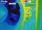
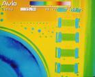
9 Key Features of SESUB Technology 1.Miniaturizing -> Help to put additional function in limited area 2. Reliable connection -> Help to improve long term reliability 8.5x8.5mm 5.6x4.6mm IC Solder WB Cu plating -65% Shrink Size or Capable to integrate more functionality WL-CSP IC QFN/QFP IC SESUB Example of Miniaturization 3. Better heat dissipation -> Help to dissipate IC heat to M/B Laminate SiP CROSS LINE SESUB SiP CROSS LINE Better Connection compared with Soldering or Wire Bonding 4. Low loss & noise emission -> Help to lower loss & noise emission (Especially digital circuit) Laminate SiP Noise emission SESUB SiP Less noise emission Tc : -6degC Signal Coupling Thermal simulation result ECBC PAF SESUB BU 9

10 1. Miniaturizing SESUB is the best solution to minimize SiP size Smart phone trend: Additional Functions in same space Or make space for Battery. To save space is requirement. -> Requirement for SiP is as small as possible ECBC PAF SESUB BU 10


 Sn IMC IMC(growth thicker) Cu Solder Ball Wire Bond +")

11 2. Reliable Connection Current solution (Solder, WB) Potential REL Failure under Stress because of IMC. IMC (Intermetallic Compound) : Composed of multiple constituents from metal and the others metal at elevated temperature. IMC growth thicker (become Fragile) Chance to crack Cause joint open failure Thermal Thermal Stress Sn Sn (reflow) Sn IMC IMC(growth thicker) Cu Solder Ball Wire Bond + REL Failure Cu TCT Cu Solder ball TCT: Temperature Cycle Test ( degc) Solder Joint IMC Sn IMC IM C Cu Au Ball Bond Joint IMC Au Au-Al IMC Al IMC IMC Crack Requested addition process (e.g. Underfill) to prevent stress to the connection Sn Crack Au Al Cu IMC Crack ECBC PAF SESUB BU 11
12 2. Reliable Connection SESUB Solution for long term Reliability Thermal Stress No chance IMC SESUB Via connection Cu Cu + Cu Cu TCT TCT: Temperature Cycle Test ( degc) Copper to Copper joint -> No IMC created (Same metal) Die Cu RDL on Chip Via (Cu plating by SESUB) Lower chance to make crack with Cu/Cu connection after Stress or Manufacturing conditions ECBC PAF SESUB BU 12
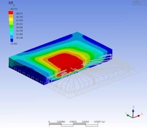
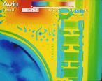
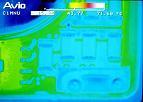
13 3. Better Heat Dissipation SESUB can help to Dissipate Heat IC Die (Top View) SESUB (Side View) Heat Spot Embedded IC die Heat Spot Cu Via Many Cu Via can be put underneath Heat Spot intentionally -> SESUB can dissipate most heat to M/B (70% by thermal simulation result) Heat Releasing Image 30% Embedded IC die Heat Spot M/B (Mother Board) Heat 70% Heat Heat from SESUB will be released by M/B Efficiently ECBC PAF SESUB BU 13

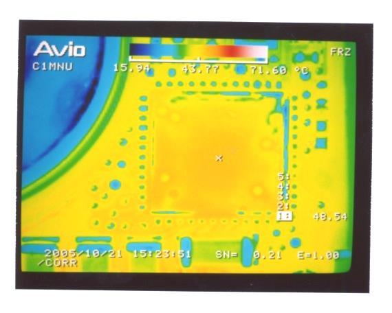
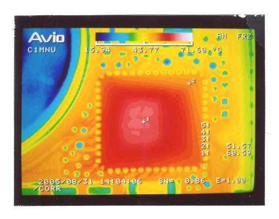
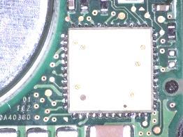
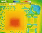
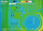

14 3. Better Heat Dissipation Example in real application QFN Package SESUB Confirmation of lower thermal resistance by measurement and simulation Thermal simulation Thermal simulation QFN Package 20 /w SESUB 5 /w t=0.9mm t=0.22mm Embedded IC die 1/4 Thickness of QFN Package Down ECBC PAF SESUB BU 14

15 4. Low loss & noise emission Redundant Parasitic for Better Performance SESUB help to good performance for Digital signals by shortest traces Laminate SiP Minimum Signal Coupling Redundant Noise Emission SESUB SiP TOP VIEW Passives TOP VIEW IC Voltage drop IC SIDE VIEW Noise emission SIDE VIEW Less noise emission Signal Coupling Large Noise Small Noise ECBC PAF SESUB BU 15
16 Contents SESUB Introduction SESUB Process SESUB Quality SESUB Potential Application Summary ECBC PAF SESUB BU 16
17 Image of IC Embedding Process EOS (Embedding Organic Sheet) is soft and flowable, before cure. It flows during laminate keeping its volume with no stress concentration. EOS2 EOS1 ECBC PAF SESUB BU 17
18 Image of IC Embedding Process Completed SESUB Symmetric structure makes SESUB flat ECBC PAF SESUB BU 18
 3.5 3.0 2.")


19 SESUB Warpage Performance (Sheet level) SESUB Warpage Over temperature Range warpage(mm) TDK internal spec. <3mm x150mm SESUB Sheet Temp (degc) in Reflow condtion Shadow Moire Module Piece Substrate Warpage is under ECBC PAF SESUB BU 19
 15μm Warpage(um) 100 90 80 70 60 50 40 30 20 10 0-10 -20-30 -40-50 -60-70 -80-90 -100 Warpage vs Teperature Warpage in Reflow Condition 30degC 220degC 260degC 220degC")
 Die size : 5.9x5.4mm, 3.2x2.3mm (80μmt) Pad Surface : Bumped LGA FCBGA : 9.0x9.0mm (reference) Package (Sub) thickness : 0.5mm (0.18mm) Die size : 5.4x4.")
20 SESUB Warpage Performance (SiP Level) Warpage in Reflow Condition Co-planarity Specification 50μm Module Size: 5.8x3.0mm Molding : Molding & Shield Module Thickness: 1.0mm Die size : 2.6x2.0mm Pad Surface : LGA (ENEPIG) 15μm Warpage(um) Warpage vs Teperature Warpage in Reflow Condition 30degC 220degC 260degC 220degC 30degC Temperature ( ) SESUB Module:11x11mm FCBGA:9x9mm(reference) 45μm Co-planarity Specification 60μm Module Size : 11.0x11.0mm Shielding : Metal Can Shield Module (Sub) thickness : 1.1mm (0.33mm) Die size : 5.9x5.4mm, 3.2x2.3mm (80μmt) Pad Surface : Bumped LGA FCBGA : 9.0x9.0mm (reference) Package (Sub) thickness : 0.5mm (0.18mm) Die size : 5.4x4.6mm (210μmt) Pad surface: BGA Module Warpage is Similar Level to Other Package with Same Size ECBC PAF SESUB BU 20

21 SESUB Robustness against Warpage What would happen, when bending SESUB? 150 x 150mm SESUB before B/E. 2x3mm Low-K bare die embedded. ECBC PAF SESUB BU 21

![Leakage I[uA] VBAT 20 19 18 17 16 15 14 13](/docs-images/92/110267214/images/22-1.jpg "12 11 10 Initial 15 10 5 2 R[cm] N=10 4 R")
 was changed from 15 to 1cm.")
22 Bending Experiment (1) Result : No failure detected at R=15 to 2cm. Leakage I[uA] VBAT Initial R[cm] N=10 4 R = 1 cm. Radius(R) was changed from 15 to 1cm. But SESUB broke at R = 1 cm. R=3cm ECBC PAF SESUB BU 22
23 Bending Experiment (2) Result : No failure detected after R=5cm,3x Bend,5x Reflow. Leakage I[uA] VBAT Initial After Bend After Reflow N=104 Sample A I[uA] VBAT Initial After Bend After Reflow N=104 Sample B Experiment Flow Sample A:Etest 1x bend (both directions) Etest 5x reflow Etest Sample B:Etest 3x bend (both directions) Etest 5x reflow Etest Bending cirteria = 5 cm radius ECBC PAF SESUB BU 23

24 Thin Si a) The thinner the chip, the more flexible it is. b) The crack happen by mechanical stress concentration. After safely embedded in SESUB, resin work as stress relief and become much stronger than die itself. ECBC PAF SESUB BU 24
25 Contents SESUB Introduction SESUB Process SESUB Quality SESUB Potential Application Summary ECBC PAF SESUB BU 25
26 TDK SESUB product has proven in the HVM Customer Assy & Test SiP SESUB Smart Phone (mid-17 to mid-18) Input > 50 Mil pcs Input > 50 Mil pcs > 50 Mil pcs Defect rate < 100 dppm Yield > 99% > 99% Competitor SiP Product Standard defect rate level : ~ 500 dppm Why Customer products can have high yield SESUB Substrate High & Stable Yield TDK can support customer s success by extensive design experiences ECBC PAF SESUB BU 26

27 SESUB Sheet Level Reliability Testing Results Item Standard Condition Criteria Result High Temp. Storage JESD22-A degC * 1000hr R increase <10% PASS High Current Test 400mA * 1000hr R increase <10% PASS Heat Shock [Liquid] IEC ~ +150degC * 3000cyc R increase <10% PASS High Temp. Humidity Bias JESD22-A degC 85%, 35V * 3000hr IR>5.0*1e8[ohm] PASS Reflow J-STD-020 MSL3 (60degC/60%RH * 40hr) 5 times reflow R increase <10% PASS ECBC PAF SESUB BU 27

28 SESUB Module Board Level Reliability Testing Results test item abbreviation standard condition Module1 Module2 Module3 Temperature Cycling TC JESD22-A104-55degC to +125degC * 850cyc PASS PASS PASS Drop test - JESD22-B g, 0.5msec * 30drops PASS PASS PASS Mechanical Shock MS MIL-STD kg, 0.25msec PASS N/A N/A Cyclic Bending - JESD22-B u strain * 25k bend PASS N/A N/A Vibration VFV JESD22-B103 5g, 1mmp-p, 5-500Hz PASS N/A N/A (30pads) ECBC PAF SESUB BU 28
29 Contents SESUB Introduction SESUB Process SESUB Quality SESUB Potential Application Summary ECBC PAF SESUB BU 29


 11.")


 Package Size")
 5.0x5.")
 5.")
30 SESUB SiP Products (All are OEM Products) Application μdcdc Buck Convertor Boost Up Converter Power Management Unit μdcdc Buck Convertor Power Supply Package Size 2.3x2.9mm (7.0mm 2 ) 2.3x2.4mm (121mm 2 ) 11.0x11.0mm (121mm 2 ) 2.5x2.0mm (7.3mm 2 ) MP Ramp 2011 / Q / Q / Q / Q2 Application Wearable Battery Charger Quick Battery Charger Envelope Tracker Wireless Power Receiver Advanced Function (Power) Package Size 2.8x2.6mm (7.3mm 2 ) 5.0x5.0mm (25mm 2 ) 5.8x3.0mm (17.7mm 2 ) 5.0x4.0mm (20mm 2 ) MP Ramp 2014/ Q4 2016/ Q / Q / Q1 ECBC PAF SESUB BU 30


31 SESUB Technology Lineup & Roadmap Layers Stack 4 Layers 2 Layers 4 Layers 6 Layers Multi chip 2 chip horizontally Multi chip horizontally Package Open Top Over Molding Shielded Over Molding Metal Can Shield Case SESUB with Thin film Capacitor Thickness 4 Layers 300um 2 Layers 250um ~220um 4 Layers 200um 2 Layers Line/Space 34/46um 15/20um Occupation ratio 15% ~ 60% 10% ~ 70% Now in MP Status in future ECBC PAF SESUB BU 31
 (Double side terminal) Much thinner Capacitor ECBC PAF SESUB BU")
32 Introduction of Thin Film Capacitor TFCP-S (Sheet type) TFCP-D (Discrete type) Cu Dielectric(BT) Ni foil Two terminal capacitor Multi terminal capacitor (Top side terminal) (Double side terminal) Much thinner Capacitor ECBC PAF SESUB BU 32
33 Contents SESUB Introduction SESUB Process SESUB Quality SESUB Potential Application Summary ECBC PAF SESUB BU 33
34 Summary SESUB key features I. Miniaturization II. Long term Reliability III. Better Heat Dissipation IV. Low loss & noise emission SESUB is already proven technology in HVM TDK has extensive layout design experience & Know-How TDK wish to co-work with customer for their product success ECBC PAF SESUB BU 34
35 Visit TDK Product Center on our web site for more detail.
The Future of Packaging ~ Advanced System Integration
 The Future of Packaging ~ Advanced System Integration Enabling a Microelectronic World R. Huemoeller SVP, Adv. Product / Platform Develop June 2013 Product Segments End Market % Share Summary 2 New Product
POSSUM TM Die Design as a Low Cost 3D Packaging Alternative
 POSSUM TM Die Design as a Low Cost 3D Packaging Alternative The trend toward 3D system integration in a small form factor has accelerated even more with the introduction of smartphones and tablets. Integration
Laminate Based Fan-Out Embedded Die Technologies: The Other Option
 Laminate Based Fan-Out Embedded Die Technologies: The Other Option Theodore (Ted) G. Tessier, Tanja Karila*, Tuomas Waris*, Mark Dhaenens and David Clark FlipChip International, LLC 3701 E University Drive
SiP packaging technology of intelligent sensor module. Tony li
 SiP packaging technology of intelligent sensor module Tony li 2016.9 Contents What we can do with sensors Sensor market trend Challenges of sensor packaging SiP technology to overcome challenges Overview
Innovative Embedded Technologies to Enable Thinner IoT/Wearable/Mobile Devices
 Innovative Embedded Technologies to Enable Thinner IoT/Wearable/Mobile Devices Jensen Tsai Deputy Director, SPIL Building a Smarter World Wearable Internet of Things Building a Smarter World Mobile Devices
Interconnection Challenge in Wire Bonding Ag alloy wire. Jensen Tsai / 蔡瀛洲, SPIL, Taiwan
 1 Interconnection Challenge in Wire Bonding Ag alloy wire Jensen Tsai / 蔡瀛洲, SPIL, Taiwan 2 Content Ag Alloy Wire Type Market Ag Alloy Wire Benefits Workability and Reliability Performance IMC behavior
Silicon Interposers enable high performance capacitors
 Interposers between ICs and package substrates that contain thin film capacitors have been used previously in order to improve circuit performance. However, with the interconnect inductance due to wire
MICROELECTRONICS ASSSEMBLY TECHNOLOGIES. The QFN Platform as a Chip Packaging Foundation
 West Coast Luncheon January 15, 2014. PROMEX PROMEX INDUSTRIES INC. MICROELECTRONICS ASSSEMBLY TECHNOLOGIES The QFN Platform as a Chip Packaging Foundation 3075 Oakmead Village Drive Santa Clara CA Ɩ 95051
!"#$"%&' ()#*+,-+.&/0(
#*+,-+.&/0(") !"#$"%&' ()#*+,-+.&/0( Multi Chip Modules (MCM) or Multi chip packaging Industry s first MCM from IBM. Generally MCMs are horizontal or two-dimensional modules. Defined as a single unit containing two
!"#$"%&' ()#*+,-+.&/0( Multi Chip Modules (MCM) or Multi chip packaging Industry s first MCM from IBM. Generally MCMs are horizontal or two-dimensional modules. Defined as a single unit containing two
The Future of Packaging and Cu Wire Bonding Advances. Ivy Qin
 The Future of Packaging and Cu Wire Bonding Advances Ivy Qin Introduction Semiconductors have been around for over 70 years Packaging is playing a more and more important role, providing low cost high
High Efficient Heat Dissipation on Printed Circuit Boards. Markus Wille, R&D Manager, Schoeller Electronics Systems GmbH
 High Efficient Heat Dissipation on Printed Circuit Boards Markus Wille, R&D Manager, Schoeller Electronics Systems GmbH m.wille@se-pcb.de Introduction 2 Heat Flux: Q x y Q z The substrate (insulation)
Packaging Technology and Design Challenges for Fine Pitch Cu Pillar and BOT (Bond on Trace) using Thermal Compression Bonding
 using Thermal Compression Bonding") Packaging Technology and Design Challenges for Fine Pitch Cu Pillar and BOT (Bond on Trace) using Thermal Compression Bonding MJ (Myung-June) Lee 1, Chew Ching Lim 2, Pheak Ti Teh 2 1: Altera Corporation,
Packaging Technology and Design Challenges for Fine Pitch Cu Pillar and BOT (Bond on Trace) using Thermal Compression Bonding MJ (Myung-June) Lee 1, Chew Ching Lim 2, Pheak Ti Teh 2 1: Altera Corporation,
Advances in stacked-die packaging
 pg.10-15-carson-art 16/6/03 4:12 pm Page 1 The stacking of die within IC packages, primarily Chip Scale Packages (CSP) Ball Grid Arrays (BGAs) has evolved rapidly over the last few years. The now standard
Image Sensor Advanced Package Solution. Prepared by : JL Huang & KingPak RD division
 Image Sensor Advanced Package Solution Prepared by : JL Huang & KingPak RD division Contents CMOS image sensor marketing overview Comparison between different type of CMOS image sensor package Overview
Smart Devices of 2025
 Smart Devices of 2025 Challenges for Packaging of Future Device Technologies Steve Riches/Kevin Cannon Tribus-D Ltd CW Workshop 27 March 2018 E:mail: info@tribus-d.uk M: 07804 980 954 Assembly Technology
Innovations Push Package-on-Package Into New Markets. Flynn Carson. STATS ChipPAC Inc Kato Rd Fremont, CA 94538
 Innovations Push Package-on-Package Into New Markets by Flynn Carson STATS ChipPAC Inc. 47400 Kato Rd Fremont, CA 94538 Copyright 2010. Reprinted from Semiconductor International, April 2010. By choosing
Technology Development & Integration Challenges for Lead Free Implementation. Vijay Wakharkar. Assembly Technology Development Intel Corporation
 Technology Development & Integration Challenges for Lead Free Implementation Vijay Wakharkar Assembly Technology Development Intel Corporation Legal Information THIS DOCUMENT AND RELATED MATERIALS AND
New Wave SiP solution for Power
 New Wave SiP solution for Power Vincent Lin Corporate R&D ASE Group APEC March 7 th, 2018 in San Antonio, Texas. 0 Outline Challenges Facing Human Society Energy, Environment and Traffic Autonomous Driving
Min Tao, Ph. D, Ashok Prabhu, Akash Agrawal, Ilyas Mohammed, Ph. D, Bel Haba, Ph. D Oct , IWLPC
 PACKAGE-ON-PACKAGE INTERCONNECT FOR FAN-OUT WAFER LEVEL PACKAGES Min Tao, Ph. D, Ashok Prabhu, Akash Agrawal, Ilyas Mohammed, Ph. D, Bel Haba, Ph. D Oct 18-20 2016, IWLPC 1 Outline Laminate to Fan-Out
WLP User's Guide. CMOS IC Application Note. Rev.1.0_03. ABLIC Inc., 2014
 CMOS IC Application Note WLP User's Guide ABLIC Inc., 2014 This document is a reference manual that describes the handling of the mounting of super-small WLP (Wafer Level Package) for users in the semiconductor
Advanced High-Density Interconnection Technology
 Advanced High-Density Interconnection Technology Osamu Nakao 1 This report introduces Fujikura s all-polyimide IVH (interstitial Via Hole)-multi-layer circuit boards and device-embedding technology. Employing
Packaging Roadmap: The impact of miniaturization. Bob Pfahl, inemi Celestica-iNEMI Technology Forum May 15, 2007
 Packaging Roadmap: The impact of miniaturization Bob Pfahl, inemi Celestica-iNEMI Technology Forum May 15, 2007 The Challenges for the Next Decade Addressing the consumer experience using the converged
Figure 1. FCBGA and fccsp Packages
 Packaging Technology and Design Challenge for Fine Pitch Micro-Bump Cu-Pillar and BOT (Direct Bond on Substrate-Trace) Using TCNCP (Thermal Compression with Non-Conductive Paste Underfill) Method *MJ (Myung-June)
AN5046 Application note
 Application note Printed circuit board assembly recommendations for STMicroelectronics PowerFLAT packages Introduction The PowerFLAT package (5x6) was created to allow a larger die to fit in a standard
Challenges of Ultra-thin LGA Package for Fingerprint Sensors
 Challenges of Ultra-thin LGA Package for Fingerprint Sensors Jensen Tsai Deputy Director, SPIL Outline Background Package Features & Challenges Challenges & Solutions Mold Clearance Low Wire Loop Height
Fraunhofer IZM - ASSID
 FRAUNHOFER-INSTITUT FÜR Zuverlässigkeit und Mikrointegration IZM Fraunhofer IZM - ASSID All Silicon System Integration Dresden Heterogeneous 3D Wafer Level System Integration 3D system integration is one
Thin Film Resistor Integration into Flex-Boards
 Thin Film Resistor Integration into Flex-Boards 7 rd International Workshop Flexible Electronic Systems November 29, 2006, Munich by Dr. Hans Burkard Hightec H MC AG, Lenzburg, Switzerland 1 Content HiCoFlex:
EMERGING SUBSTRATE TECHNOLOGIES FOR PACKAGING
 EMERGING SUBSTRATE TECHNOLOGIES FOR PACKAGING Henry H. Utsunomiya Interconnection Technologies, Inc. Suwa City, Nagano Prefecture, Japan henryutsunomiya@mac.com ABSTRACT This presentation will outline
Design and Development of True-CSP
 Design and Development of True-CSP *Kolan Ravi Kanth, Francis K.S. Poh, B.K. Lim, Desmond Y.R. Chong, Anthony Sun, H.B. Tan United Test & Assembly Center Ltd (UTAC) 5 Serangoon North Ave 5, Singapore 554916
Introduction of IMS Technology for Advanced Solder Bumping on Wafers / Laminates
 Introduction of IMS Technology for Advanced Solder Bumping on Wafers / Laminates Science & Technology IBM Research Tokyo Yasumitsu Orii, PhD Senju Metal Industry Co.,TW Deputy General Manager Lewis Huang
The 3D Silicon Leader
 The 3D Silicon Leader 3D Silicon IPD for smaller and more reliable Implantable Medical Devices ATW on Advanced Packaging for Wireless Medical Devices Mohamed Mehdi Jatlaoui, Sébastien Leruez, Olivier Gaborieau,
FBTI Flexible Bumped Tape Interposer
 FBTI Flexible Bumped Tape Interposer Development of FBTI (Flexible Bumped Tape Interposer) * * * * *2 Kazuhito Hikasa Toshiaki Amano Toshiya Hikami Kenichi Sugahara Naoyuki Toyoda CSPChip Size Package
Organic Packaging Substrate Workshop Overview
 Organic Packaging Substrate Workshop Overview Organized by: International Electronics Manufacturing Initiative (inemi) Mario A. Bolanos November 17-18, 2009 1 Organic Packaging Substrate Workshop Work
2.5D Platform (Examples of products produced to date are shown here to demonstrate Amkor's production capabilities)
") Wafer Finishing & Flip Chip Stacking interconnects have emerged to serve a wide range of 2.5D- & 3D- packaging applications and architectures that demand very high performance and functionality at the
Wafer Finishing & Flip Chip Stacking interconnects have emerged to serve a wide range of 2.5D- & 3D- packaging applications and architectures that demand very high performance and functionality at the
EMBEDDED ACTIVE DEVICE PACKAGING TECHNOLOGY FOR REAL DDR2 MEMORY CHIPS
 EMBEDDED ACTIVE DEVICE PACKAGING TECHNOLOGY FOR REAL DDR2 MEMORY CHIPS Yin-Po Hung, Tao-Chih Chang, Ching-Kuan Lee, Yuan-Chang Lee, Jing-Yao Chang, Chao-Kai Hsu, Shu-Man Li, Jui-Hsiung Huang, Fang-Jun
Substrates Lost in Translation
 2004 IEEE PRESENTATION Components, Packaging & Manufacturing Technology (CPMT) Society, Santa Clara Valley Chapter www.cpmt.org/scv/ Substrates Lost in Translation R. Huemoeller Vice President, Substrate
Fan-Out Wafer Level Packaging Patent Landscape Analysis
 Fan-Out Wafer Level Packaging Patent Landscape Analysis Source: Infineon Source: TSMC Source: ASE November 2016 Source: Deca Technologies Source: STATS ChipPAC Source: Nepes KnowMade Patent & Technology
BGA (Ball Grid Array)
") BGA (Ball Grid Array) National Semiconductor Application Note 1126 November 2002 Table of Contents Introduction... 2 Package Overview... 3 PBGA (PLASTIC BGA) CONSTRUCTION... 3 TE-PBGA (THERMALLY ENHANCED
BGA (Ball Grid Array) National Semiconductor Application Note 1126 November 2002 Table of Contents Introduction... 2 Package Overview... 3 PBGA (PLASTIC BGA) CONSTRUCTION... 3 TE-PBGA (THERMALLY ENHANCED
mcube LGA Package Application Note
 AN-001 Rev.02 mcube LGA Package Application Note AN-001 Rev.02 mcube, Inc. 1 / 21 AN-001 Rev.02 Guidelines for Printed Circuit Board (PCB) Design and Assembly with mcube Land Grid Array (LGA) Package Sensors
TOLERANCE FORGOTTEN: IMPACTS OF TODAY S COMPONENT PACKAGING AND COPPER ROUTING ON ELECTRONIC
 TOLERANCE FORGOTTEN: IMPACTS OF TODAY S COMPONENT PACKAGING AND COPPER ROUTING ON ELECTRONIC Presented By: Dale Lee E-mail: Dale.Lee@Plexus.Com April 2013 High Layer Counts Wide Range Of Component Package
Handling, soldering & mounting instructions
 Multiple inertial measurement units: Document revision 1.2 Document release date January 2018 Document number BST-MIS-HS000-01 Technical reference code Notes 0 273 141 134 0 273 141 221 0 273 141 365 0
SOLDERABLE ANISOTROPIC CONDUCTIVE ADHESIVES FOR 3D PACKAGE APPLICATIONS
 SOLDERABLE ANISOTROPIC CONDUCTIVE ADHESIVES FOR 3D PACKAGE APPLICATIONS ABSTRACT: Dr. Mary Liu and Dr. Wusheng Yin YINCAE Advanced Materials, LLC Albany, NY 3D packaging has recently become very attractive
Brief Introduction of Sigurd IC package Assembly
 Brief Introduction of Sigurd IC package Assembly Content Package Development Trend Product Brief Sawing type QFN Representative MEMS Product LGA Light Sensor Proximity Sensor High Yield Capability Low
Advanced Wafer Level Packaging of RF-MEMS with RDL Inductor
 Advanced Wafer Level Packaging of RF-MEMS with RDL Inductor Paul Castillou, Roberto Gaddi, Rob van Kampen, Yaojian Lin*, Babak Jamshidi** and Seung Wook Yoon*** Cavendish Kinetics, 2960 North First Street,
Compression Molding. Solutions for 3D TSV and other advanced packages as well as cost savings for standard package applications
 Compression Molding Solutions for 3D TSV and other advanced packages as well as cost savings for standard package applications 1. Company Introduction 2. Package Development Trend 3. Compression FFT Molding
High efficient heat dissipation on printed circuit boards
 High efficient heat dissipation on printed circuit boards Figure 1: Heat flux in a PCB Markus Wille Schoeller Electronics Systems GmbH www.schoeller-electronics.com Abstract This paper describes various
Encapsulated Wafer Level Chip Scale Package (ewlcsp ) for Cost Effective and Robust Solutions in FlexLine
 for Cost Effective and Robust Solutions in FlexLine") Encapsulated Wafer Level Chip Scale Package (ewlcsp ) for Cost Effective and Robust Solutions in FlexLine by Yaojian Lin, Kang Chen, Kian Meng Heng, Linda Chua and *Seung Wook Yoon STATS ChipPAC Ltd. 5
Encapsulated Wafer Level Chip Scale Package (ewlcsp ) for Cost Effective and Robust Solutions in FlexLine by Yaojian Lin, Kang Chen, Kian Meng Heng, Linda Chua and *Seung Wook Yoon STATS ChipPAC Ltd. 5
Monolithic Amplifier CMA-103+ Ultra Linear Low Noise, Ceramic to 4 GHz
 Ultra Linear Low Noise, Ceramic Monolithic Amplifier 50Ω 0.05 to 4 GHz The Big Deal Ceramic, hermetically sealed, nitrogen filled Low profile case, 0.045 Ultra High IP3 Broadband High Dynamic Range CASE
Yole Developpement. Developpement-v2585/ Publisher Sample
 Yole Developpement http://www.marketresearch.com/yole- Developpement-v2585/ Publisher Sample Phone: 800.298.5699 (US) or +1.240.747.3093 or +1.240.747.3093 (Int'l) Hours: Monday - Thursday: 5:30am - 6:30pm
Two major features of this text
 Two major features of this text Since explanatory materials are systematically made based on subject examination questions, preparation
Surface Mount Header Assembly Employs Capillary Action
 New Product Technology Surface Mount Header Assembly Employs Capillary Action Zierick s unique header assembly features capillary action to improve solder joint strength. As a result, pin retention force
PKF series. General information. PKF series
 PKF series PKF series General information SMD and through hole versions with ultra-low component height 8.0 mm (0.315 in.) Up to 87% efficiency at full load Safety requirements in accordance with EN60950
New Approaches to Develop a Scalable 3D IC Assembly Method
 New Approaches to Develop a Scalable 3D IC Assembly Method Charles G. Woychik Ph.D. Sangil Lee, Ph.D., Scott McGrath, Eric Tosaya and Sitaram Arkalgud Ph.D. Invensas Corporation 3025 Orchard Parkway San
10nm CPI Study for Fine Pitch Flip Chip Attach Process and Substrate
 10nm CPI Study for Fine Pitch Flip Chip Attach Process and Substrate Ming-Che Hsieh, Chi-Yuan Chen*, Ian Hsu*, Stanley Lin* and KeonTaek Kang** Product and Technology Marketing / STATS ChipPAC Pte. Ltd.
Fan-Out Solutions: Today, Tomorrow the Future Ron Huemoeller
 Fan-Out Solutions: Today, Tomorrow the Future Ron Huemoeller Corporate Vice President, WW RnD & Technology Strategy 1 In the Beginning ewlb 2 Fan Out Packaging Emerges Introduction of Fan Out (ewlb) Marketed
FO-WLP, Embedded Die, and Alternatives: Market Trends and Drivers
 FO-WLP, Ebedded Die, and Alternatives: Market Trends and Drivers www.techsearchinc.co Many Package Choices: Which One is the Correct Choice? FO-WLP (chip-last, chip-first, face-up, face-down) Traditional
mcube WLCSP Application Note
 AN-002 Rev.02 mcube WLCSP Application Note AN-002 Rev.02 mcube, Inc. 1 / 20 AN-002 Rev.02 Guidelines for Printed Circuit Board (PCB) Design and Assembly with mcube Wafer Level Chip Scale Package (WLCSP)
TAIPRO Engineering. Speaker: M. Saint-Mard Managing director. TAIlored microsystem improving your PROduct
 TAIPRO Engineering MEMS packaging is crucial for system performance and reliability Speaker: M. Saint-Mard Managing director TAIPRO ENGINEERING SA Michel Saint-Mard Administrateur délégué m.saintmard@taipro.be
HSNT Package User's Guide
 CMOS IC Application Note HSNT Package User's Guide ABLIC Inc., 2011-2014 This manual describes the features, package dimensions, recommended land, handling methods as well as marking specifications and
Data Sheet _ R&D. Rev Date: 8/17
 Data Sheet _ R&D Rev Date: 8/17 Micro Bump In coming years the interconnect density for several applications such as micro display, imaging devices will approach the pitch 10um and below. Many research
BCD Smart Power Roadmap Trends and Challenges. Giuseppe Croce NEREID WORKSHOP Smart Energy Bertinoro, October 20 th
 BCD Smart Power Roadmap Trends and Challenges Giuseppe Croce NEREID WORKSHOP Smart Energy Bertinoro, October 20 th Outline 2 Introduction Major Trends in Smart Power ASICs An insight on (some) differentiating
AltiumLive 2017: Creating Documentation for Successful PCB Manufacturing
 AltiumLive 2017: Creating Documentation for Successful PCB Manufacturing Julie Ellis TTM Field Applications Engineer Thomas Schneider Field Applications Engineer 1 Agenda 1 Complexity & Cost 2 3 4 5 6
B. Flip-Chip Technology
 B. Flip-Chip Technology B1. Level 1. Introduction to Flip-Chip techniques B1.1 Why flip-chip? In the development of packaging of electronics the aim is to lower cost, increase the packaging density, improve
3D ICs: Recent Advances in the Industry
 3D ICs: Recent Advances in the Industry Suresh Ramalingam Senior Director, Advanced Packaging Outline 3D IC Background 3D IC Technology Development Summary Acknowledgements Stacked Silicon Interconnect
Stack Die CSP Interconnect Challenges Flynn Carson, Glenn Narvaez, HC Choi, and DW Son ChipPAC, Inc.
 Stack Die CSP Interconnect Challenges Flynn Carson, Glenn Narvaez, HC Choi, and DW Son ChipPAC, Inc. IEEE/CPMT Seminar Overview 4 Stacked die Chip Scale Packages (CSPs) enable more device functionality
Thermal Cycling and Fatigue
 Thermal Cycling and Fatigue Gil Sharon Introduction The majority of electronic failures are thermo-mechanically related by thermally induced stresses and strains. The excessive difference in coefficients
SNT Package User's Guide
 (Small outline Non-leaded Thin package) [Target Packages] SNT-4A SNT-6A SNT-6A (H) SNT-8A SNT Package User s Guide Introduction This manual describes the features, dimensions, mountability, reliability,
TSV MEOL (Mid-End-Of-Line) and its Assembly/Packaging Technology for 3D/2.5D Solutions
 and its Assembly/Packaging Technology for 3D/2.5D Solutions") TSV MEOL (Mid-End-Of-Line) and its Assembly/Packaging Technology for 3D/2.5D Solutions Seung Wook YOON, D.J. Na, *K. T. Kang, W. K. Choi, C.B. Yong, *Y.C. Kim and Pandi C. Marimuthu STATS ChipPAC Ltd.
TSV MEOL (Mid-End-Of-Line) and its Assembly/Packaging Technology for 3D/2.5D Solutions Seung Wook YOON, D.J. Na, *K. T. Kang, W. K. Choi, C.B. Yong, *Y.C. Kim and Pandi C. Marimuthu STATS ChipPAC Ltd.
Low-Cost PCB Design 1
 Low-Cost PCB Design 1 PCB design parameters Defining PCB design parameters begins with understanding: End product features, uses, environment, and lifetime goals PCB performance, manufacturing, and yield
Advanced Embedded Packaging for Power Devices
 2017 IEEE 67th Electronic Components and Technology Conference Advanced Embedded Packaging for Power Devices Naoki Hayashi, Miki Nakashima, Hiroshi Demachi, Shingo Nakamura, Tomoshige Chikai, Yukari Imaizumi,
Specifications subject to change Packaging
 VCSEL Standard Product Packaging Options All standard products are represented in the table below. The Part Number for a standard product is determined by replacing the x in the column Generic Part Number
An Introduction to Electronics Systems Packaging. Prof. G. V. Mahesh. Department of Electronic Systems Engineering
 An Introduction to Electronics Systems Packaging Prof. G. V. Mahesh Department of Electronic Systems Engineering India Institute of Science, Bangalore Module No. # 02 Lecture No. # 08 Wafer Packaging Packaging
Z-Axis Power Delivery (ZAPD) Concept and Implementation
 Concept and Implementation") Z-Axis Power Delivery (ZAPD) Concept and Implementation 1 The Slew Rate Wall < 20pH < 20pH Beyond 2005 di/dt = 1000 A/ns V droop = 75 mv 2004 di/dt =680 A/ns V droop = 100 mv 1500pH 500pH 2003 di/dt =
Z-Axis Power Delivery (ZAPD) Concept and Implementation 1 The Slew Rate Wall < 20pH < 20pH Beyond 2005 di/dt = 1000 A/ns V droop = 75 mv 2004 di/dt =680 A/ns V droop = 100 mv 1500pH 500pH 2003 di/dt =
Power Integration in Circuit Board
 Power Integration in Circuit Board APEC 2015 AT & S Austria Technologie & Systemtechnik Aktiengesellschaft Fabriksgasse13 A-8700 Leoben Tel +43 (0) 3842 200-0 E-Mail info@ats.net www.ats.net PICB APEC
1. Exceeding these limits may cause permanent damage.
 Silicon PIN Diode s Features Switch & Attenuator Die Extensive Selection of I-Region Lengths Hermetic Glass Passivated CERMACHIP Oxide Passivated Planar s Voltage Ratings to 3000V Faster Switching Speed
COPYRIGHT 2013 LED ENGIN. ALL RIGHTS RESERVED. LZ1-00R500 (1.0 08/23/13)
") 940nm Infrared LED Emitter LZ1-00R500 Key Features High Efficacy 940nm 2W Infrared LED Ultra-small foot print 4.4mm x 4.4mm Surface mount ceramic package with integrated glass lens Very low Thermal Resistance
940nm Infrared LED Emitter LZ1-00R500 Key Features High Efficacy 940nm 2W Infrared LED Ultra-small foot print 4.4mm x 4.4mm Surface mount ceramic package with integrated glass lens Very low Thermal Resistance
Monolithic Amplifier CMA-162LN+ Ultra Low Noise, High IP to 1.6 GHz
 Ultra Low Noise, High IP3 Monolithic Amplifier 50Ω 0.7 to 1.6 GHz The Big Deal Ceramic, Hermetically Sealed, Nitrogen filled Low profile case,.045 high Ultra Low Noise Figure, 0.5 High Gain, High IP3 Class
High Average Power Handling: High Peak Power Handling: Low Insertion Loss: Low Flat Leakage Power:
 PRELIMINARY RFLM-301511QC-290 Quasi Active High Power UHF Band Limiter Module Features: Frequency Range: High Average Power Handling: High Peak Power Handling: Low Insertion Loss: Return Loss: Low Flat
High Density Interconnect on Flexible Substrate
 High Density Interconnect on Flexible Substrate Dr. C Q Cui Compass Technology Co., Ltd Shatin, HK June 9, 2004 SCV CPMT Society Chapter Meeting Compass Technology Co Ltd Founded: June, 1997 Will be listed
Innovations in EDA Webcast Series
 Welcome Innovations in EDA Webcast Series August 2, 2012 Jack Sifri MMIC Design Flow Specialist IC, Laminate, Package Multi-Technology PA Module Design Methodology Realizing the Multi-Technology Vision
High Average Power Handling: High Peak Power Handling: Low Insertion Loss: Low Flat Leakage Power:
 PRELIMINARY RFLM-301511QC-290 Quasi Active High Power UHF Band Limiter Module Features: Frequency Range: High Average Power Handling: High Peak Power Handling: Low Insertion Loss: Return Loss: Low Flat
MicroSiP TM DC/DC Converters Fully Integrated Power Solutions
 MicroSiP TM DC/DC Converters Fully Integrated Power Solutions PicoStar TM Christophe Vaucourt Thies Puchert, Udo Ottl, Frank Stepniak, Florian Feckl 1 Outline Illustrate TI s recent developments in the
Quasi Active High Power L Band PIN Diode Limiter Module - SMT. Surface Mount L- Band Limiter Module: High Peak Power Handling: Low Insertion Loss:
 PRELIMINARY RFLM-102202XA-150 Quasi Active High Power L Band PIN Diode Limiter Module - SMT Features: Surface Mount L- Band Limiter Module: Frequency Range: High Average Power Handling: High Peak Power
System in Package Workshop
 TWI, Granta Park, Abington, Cambridge 12th December 2007 The IeMRC s System in Package Workshop took place on 12 th December 2007 at TWI s Granta Park facility near Cambridge. The event was opened by Dr
Sectional Design Standard for High Density Interconnect (HDI) Printed Boards
 Printed Boards") IPC-2226 ASSOCIATION CONNECTING ELECTRONICS INDUSTRIES Sectional Design Standard for High Density Interconnect (HDI) Printed Boards Developed by the HDI Design Subcommittee (D-41) of the HDI Committee
IPC-2226 ASSOCIATION CONNECTING ELECTRONICS INDUSTRIES Sectional Design Standard for High Density Interconnect (HDI) Printed Boards Developed by the HDI Design Subcommittee (D-41) of the HDI Committee
Fine Pitch Cu Pillar Assembly Challenges for Advanced Flip Chip Package
 Fine Pitch Cu Pillar Assembly Challenges for Advanced Flip Chip Package by Nokibul Islam and Vinayak Pandey, STATS ChipPAC, Inc. Ming-Che Hsieh, STATS ChipPAC Pte. Ltd. Kang Keon Taek, STATS ChipPAC Korea
EUFANET Toulouse conferences, November 28th-29th, 2011 Stéphane Bellenger, IPDiA
 3D low-profile Silicon interposer using Passive Integration (PICS) and Advanced Packaging Solutions EUFANET Toulouse conferences, November 28th-29th, 2011 Stéphane Bellenger, IPDiA 3D Advanced Integration
Monolithic Amplifier CMA-81+ Wideband, High Dynamic Range, Ceramic. DC to 6 GHz. The Big Deal
 Wideband, High Dynamic Range, Ceramic Monolithic Amplifier 50Ω DC to 6 GHz The Big Deal Ceramic, hermetically sealed, nitrogen filled Low profile case, 0.045 High IP3, +38 m High POUT, +19.5 m CASE STYLE:
3D TSV Micro Cu Column Chip-to-Substrate/Chip Assmbly/Packaging Technology
 3D TSV Micro Cu Column Chip-to-Substrate/Chip Assmbly/Packaging Technology by Seung Wook Yoon, *K. T. Kang, W. K. Choi, * H. T. Lee, Andy C. B. Yong and Pandi C. Marimuthu STATS ChipPAC LTD, 5 Yishun Street
PAGE 1/6 ISSUE SERIES Micro-SPDT PART NUMBER R516 XXX 10X. (All dimensions are in mm [inches]) R 516 _ 1 0 _
![PAGE 1/6 ISSUE SERIES Micro-SPDT PART NUMBER R516 XXX 10X. (All dimensions are in mm [inches]) R 516 _ 1 0 _](/thumbs/96/127769340.jpg "PAGE 1/6 ISSUE SERIES Micro-SPDT PART NUMBER R516 XXX 10X. (All dimensions are in mm [inches]) R 516 _ 1 0 _") PAGE 1/6 ISSUE 15-10-18 SERIES Micro-SPDT PART NUMBER R516 XXX 10X R516 series: the RAMSES concept merges with the SLIM LINE technology, breaking up the frequency limits of SMT switches : - FULL SMT TECHNOLOGY
PAGE 1/6 ISSUE 15-10-18 SERIES Micro-SPDT PART NUMBER R516 XXX 10X R516 series: the RAMSES concept merges with the SLIM LINE technology, breaking up the frequency limits of SMT switches : - FULL SMT TECHNOLOGY
(LRP) Metal Strip Chip High Power Low Ohmic Resistor. Token Electronics Industry Co., Ltd. Version: January 12, Web:
 Metal Strip Chip High Power Low Ohmic Resistor. Token Electronics Industry Co., Ltd. Version: January 12, Web:") Version: January 12, 2017 (LRP) Metal Strip Chip High Power Low Ohmic Resistor Token Electronics Industry Co., Ltd. Web: www.token.com.tw Email: rfq@token.com.tw Taiwan: No.137, Sec. 1, Zhongxing Rd.,
Version: January 12, 2017 (LRP) Metal Strip Chip High Power Low Ohmic Resistor Token Electronics Industry Co., Ltd. Web: www.token.com.tw Email: rfq@token.com.tw Taiwan: No.137, Sec. 1, Zhongxing Rd.,
Study on Solder Joint Reliability of Fine Pitch CSP
 As originally published in the IPC APEX EXPO Conference Proceedings. Study on Solder Joint Reliability of Fine Pitch CSP Yong (Hill) Liang, Hank Mao, YongGang Yan, Jindong (King) Lee. AEG, Flextronics
2.4 GHz SMD On-Ground Antenna
 2.4 GHz SMD On-Ground Antenna Mads Sager Antenna Technology Manager Commercial Products Division Template 2.2 Featuring high performance levels and easy integration to satisfy the demands of the wireless
Quasi Active High Power L Band PIN Diode Limiter Module - SMT. Surface Mount L- Band Limiter Module: High Peak Power Handling:
 RELEASED RFLM-102202QX-290 Quasi Active High Power L Band PIN Diode Limiter Module - SMT Features: Surface Mount L- Band Limiter Module: Frequency Range: High Average Power Handling: High Peak Power Handling:
Monolithic Amplifier CMA-84+ Wideband, High Dynamic Range, Ceramic. DC to 7 GHz. The Big Deal
 Wideband, High Dynamic Range, Ceramic Monolithic Amplifier 50Ω DC to 7 GHz The Big Deal Ceramic, hermetically sealed, nitrogen filled Low profile case, 0.045 High IP3, +38 dbm High Gain, 24 db High POUT,
The RFLM102202QX-290 Limiter Module carries a Class 0 ESD rating (HBM) and an MSL 1 moisture rating.
 and an MSL 1 moisture rating.") PRELIMINARY RFLM-102202QX-290 PIN Diode Limiter Module - SMT Features: Surface Mount L- Band Limiter Module 5mm x 8mm x 2.5mm Quasi Active High Power PIN Limiter Design Frequency Range: 1 to 2 GHz High
PRELIMINARY RFLM-102202QX-290 PIN Diode Limiter Module - SMT Features: Surface Mount L- Band Limiter Module 5mm x 8mm x 2.5mm Quasi Active High Power PIN Limiter Design Frequency Range: 1 to 2 GHz High
Novel Substrate with Combined Embedded Capacitance and Resistance for Better Electrical Performance and Higher Integration
 Novel Substrate with Combined Embedded Capacitance and Resistance for Better Electrical Performance and Higher Integration John Andresakis, Pranabes Pramanik Oak-Mitsui Technologies, LLC Dan Brandler,
High Average Power Handling: High Peak Power Handling: Low Insertion Loss:
 RELEASED RFLM-102202QX-290 Quasi Active PIN Diode Limiter Module - SMT Features: Surface Mount L- Band Limiter Module Frequency Range: High Average Power Handling: High Peak Power Handling: Low Insertion
A new tool for next generation power semiconductors
 A new tool for next generation power semiconductors Cassandra Melvin / SEMICON China / Mach 16, 2018 Technology for tomorrow's solutions Contents 1. HEV/EV market growth 2. Power module packaging 3. EmPower
HOW DOES PRINTED SOLDER PASTE VOLUME AFFECT SOLDER JOINT RELIABILITY?
 HOW DOES PRINTED SOLDER PASTE VOLUME AFFECT SOLDER JOINT RELIABILITY? ABSTRACT Printing of solder paste and stencil technology has been well studied and many papers have been presented on the topic. Very