TESTABLE VLSI CIRCUIT DESIGN FOR CELLULAR ARRAYS
|
|
|
- Kelly McKinney
- 5 years ago
- Views:
Transcription
1 SENIOR DESIGN PROJECT PROPOSAL
2 PROJECT SUMMARY The main objective of this project is to design testability features that can potentially be included in any CMOS chip. For this particular design a 4-bit x 4-bit multiplier will be the circuit used to test the designed testability features. The relevance of this project is not to test the cells of a 4-bit x 4-bit multiplier or a 4-bit x 4-bit multiplier itself. The purpose of this project is to design a system that can be fabricated on a chip so that the main function of that chip can be tested with a minimal amount of external hardware or software. Testability of a chip plays a key role in the use and repair of PCBs. If a single button can be pushed to test a chip on a board, then a very powerful tool has been created. If onchip testing features say a chip is bad, then only that chip needs to be replaced, not the entire PCB. Again the purpose of this project is to develop an easy method for finding a bad chip, not to test a single cell of a cellular array. DETAILED DESCRIPTION The VLSI design of the 4-bit x 4-bit multiplier circuit will contain sixteen cells. The testing features consist of a sequence generator and an 8-bit register for a signature analysis. The multiplier will have a total of eight inputs and eight outputs. The sequence generator, controlled by a clock and a start bit, will be used for cellular testing. The outputs of the sequence generator will be given to the user. Therefore, the user will know the expected outputs of the multiplier based upon the multiplier truth table. The 8-bit register will be used to store the information provided from the test. Outputs will also come from the register for easy observation of the test's results. The importance of this project is to show the amount of hardware that could potentially be needed to fully test a chip, and reduce that hardware by implementing VLSI and digital design rules to develop on-chip testing features. The following are descriptions of the corresponding labels for the BLOCK DIAGRAM: CELLS 1 THROUGH 16 These sixteen identical cells are the basis of the 4-bit x 4-bit multiplier circuit. These cells will be designed using basic CMOS techniques. A) 4 x 4 MULTIPLIER INPUTS
3 These are the external inputs to the 4-bit x 4-bit multiplier circuit. These connections will also be used internally as the inputs from the sequence generator to test the function of the 4 x 4 multiplier when the chip is in test mode. B) 4 x 4 MULTIPLIER OUTPUTS These pins are reserved for the outputs of the 4-bit x 4-bit multiplier circuit. These connections are also used internally to supply an input to the registers when the chip is in test mode. C) SEQUENCE GENERATOR START BIT When set, the chip will begin its own diagnostic functions which will consist of a series of 8-bit words, known to the user, sent from the sequence generator to the inputs of the 4-bit x 4-bit multiplier. The external inputs and outputs will be disregarded. D) SEQUENCE GENERATOR CLOCK This pin is reserved for an external clock. This clock drives the sequence generator and the registers. E) SEQUENCE GENERATOR OUTPUTS These outputs will consist of 8-bit words used as inputs for the 4-bit x 4-bit multiplier when the chip is in test mode. These outputs will be given to the user. The sequence generator will be designed using CMOS techniques. F) REGISTER INPUTS The 8-bit register is used to store the outputs from the 4-bit x 4-bit multiplier when the chip is in test mode. The user will know the outputs from the sequence generator to the multiplier, and therefore will also know the expected outputs from the multiplier. The outputs from the multiplier are stored in the register because the test verifies many different outputs based upon many different input combinations. Since the test is clock driven the register allows for easy viewing of multiple test results. The register will also be designed using CMOS techniques. G) REGISTER OUTPUTS Comparing these outputs with the expected outputs from the 4 x 4 multiplier will give the results of the test. H) VOLTAGE SUPPLY I) GROUND
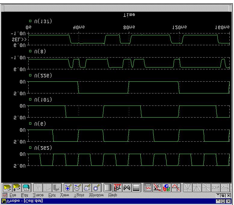
4 The LOGIC WORKS SIMULATION is an example of pre-design work. Logic Works is used to test a design before proceeding to the CMOS design stage. The CMOS DESIGN USING L-EDIT shows the CMOS design stage. This particular design is the final design of the 4-bit x 4-bit multiplier cell. The next design stage is to simulate the CMOS design using PSPICE. The PSPICE SIMULATION shows the final simulation of the 4-bit x 4-bit multiplier cell. These three main stages of design will be used throughout the duration of the project. To test the testability features after the fabrication process the 4-bit x 4-bit multiplier will first be tested manually without the testability features in use. Then the 4-bit x 4-bit multiplier will be tested using the testing features. If the results of the test using the testing features match the results of the manual test of the 4-bit x 4-bit multiplier then the testing features work properly. SCHEDULE COMPLETED TASKS: Jarrod Luker 4-bit x 4-bit multiplier cell designed CMOS 4-bit x 4-bit multiplier cell designed using L-EDIT CMOS 4-bit x 4-bit multiplier designed using L-EDIT TASKS TO BE COMPLETED: Jarrod Luker 12/03/98 Design of and Logic Works simulation of sequence generator 01/21/99 CMOS design of sequence generator 01/28/99 Continuation of CMOS design of sequence generator 02/04/99 PSPICE simulation of sequence generator completed 02/11/99 Finalize completed design to be sent for fabrication on 02/17/98 02/19/99 Start hardware design for bit x 4-bit multiplier cell designed 4-bit x 4-bit multiplier simulated using Logic Works CMOS 4-bit x 4-bit multiplier cell simulated using PSPICE CMOS 4-bit x 4-bit multiplier simulated using PSPICE 12/03/98 Design of and Logic Works simulation of 8-bit register 01/21/99 CMOS design of 8-bit register 01/28/99 Continuation of CMOS design of 8-bit register 02/04/99 PSPICE simulation of 8-bit register completed 02/11/99 Finalize completed design to be sent for fabrication on 02/17/98 02/19/99 Start hardware design for 1999
5 Research/Creative Production 02/26/99 03/05/99 03/12/99 03/19/99 03/26/99 04/02/99 Finalize work for Production 04/09/99 Begin work on final presentation 04/16/99 Continue work on final presentation 04/23/99 Continue work on final presentation 04/30/99 Finalize final presentation Research/Creative Production 02/26/99 03/05/99 03/12/99 03/19/99 03/26/99 04/02/99 Finalize work for Production 04/09/99 Begin work on final report 04/16/99 Continue work on final report 04/23/99 Continue work on final report 04/30/99 Finalize final report REFERENCES MOSIS Program. Some design rules provided by the MOSIS Program (i.e. transistor models) Mukherjee, Amar. Introduction to NMOS & CMOS VLSI Systems Design. New Jersey: P T R Prentice-Hall, Inc Prasad, Dr. V. In order to increase the chances of a successful fabrication, Dr. V. Prasad has supplied previously tested and fabricated logic gates for use in this design. Uyemura, John P. Physical Design of CMOS Integrated Circuits Using L-EDIT TM. Boston: PWS Publishing Company
6 BLOCK DIAGRAM A H I G CELL 1 CELL 5 CELL 2 CELL 3 CELL 4 CELL 6 CELL 7 CELL 8 F REGISTERS A CELL 9 CELL 10 CELL 11 CELL 12 CELL 13 CELL 14 CELL 15 CELL 16 E SEQUENCE GENERATOR B C D

7 LOGIC WORKS SIMULATION

8 CMOS DESIGN USING L-EDIT
9 PSPICE SIMULATION
VLSI Implementation & Design of Complex Multiplier for T Using ASIC-VLSI
 International Journal of Electronics Engineering, 1(1), 2009, pp. 103-112 VLSI Implementation & Design of Complex Multiplier for T Using ASIC-VLSI Amrita Rai 1*, Manjeet Singh 1 & S. V. A. V. Prasad 2
CMOS Digital Logic Design with Verilog. Chapter1 Digital IC Design &Technology
 CMOS Digital Logic Design with Verilog Chapter1 Digital IC Design &Technology Chapter Overview: In this chapter we study the concept of digital hardware design & technology. This chapter deals the standard
EE 434 ASIC & Digital Systems
 EE 434 ASIC & Digital Systems Dae Hyun Kim EECS Washington State University Spring 2017 Course Website http://eecs.wsu.edu/~ee434 Themes Study how to design, analyze, and test a complex applicationspecific
A SUBSTRATE BIASED FULL ADDER CIRCUIT
 International Journal on Intelligent Electronic System, Vol. 8 No.. July 4 9 A SUBSTRATE BIASED FULL ADDER CIRCUIT Abstract Saravanakumar C., Senthilmurugan S.,, Department of ECE, Valliammai Engineering
Academic Course Description
 BEC702 Digital CMOS VLSI Academic Course Description BHARATH UNIVERSITY Faculty of Engineering and Technology Department of Electronics and Communication Engineering BEC702 Digital CMOS VLSI Seventh Semester
EC 1354-Principles of VLSI Design
 EC 1354-Principles of VLSI Design UNIT I MOS TRANSISTOR THEORY AND PROCESS TECHNOLOGY PART-A 1. What are the four generations of integrated circuits? 2. Give the advantages of IC. 3. Give the variety of
Lab 7 (Hands-On Experiment): CMOS Inverter, NAND Gate, and NOR Gate
: CMOS Inverter, NAND Gate, and NOR Gate") Lab 7 (Hands-On Experiment): CMOS Inverter, NAND Gate, and NOR Gate EECS 170LB, Wed. 5:00 PM TA: Elsharkasy, Wael Ryan Morrison Buu Truong Jonathan Lam 03/05/14 Introduction The purpose of this lab is
Lab 7 (Hands-On Experiment): CMOS Inverter, NAND Gate, and NOR Gate EECS 170LB, Wed. 5:00 PM TA: Elsharkasy, Wael Ryan Morrison Buu Truong Jonathan Lam 03/05/14 Introduction The purpose of this lab is
Investigation on Performance of high speed CMOS Full adder Circuits
 ISSN (O): 2349-7084 International Journal of Computer Engineering In Research Trends Available online at: www.ijcert.org Investigation on Performance of high speed CMOS Full adder Circuits 1 KATTUPALLI
Academic Course Description. BEC702 Digital CMOS VLSI
 BEC702 Digital CMOS VLSI Academic Course Description Course (catalog) description BHARATH UNIVERSITY Faculty of Engineering and Technology Department of Electronics and Communication Engineering CMOS is
POWER EFFICIENT DESIGN OF COUNTER ON.12 MICRON TECHNOLOGY
 Volume-, Issue-, March 2 POWER EFFICIENT DESIGN OF COUNTER ON.2 MICRON TECHNOLOGY Simmy Hirkaney, Sandip Nemade, Vikash Gupta Abstract As chip manufacturing technology is suddenly on the threshold of major
nmos, pmos - Enhancement and depletion MOSFET, threshold voltage, body effect
 COURSE DELIVERY PLAN - THEORY Page! 1 of! 7 Department of Electronics and Communication Engineering B.E/B.Tech/M.E/M.Tech : EC Regulation: 2016(Autonomous) PG Specialization : Not Applicable Sub. Code
Exercise 1: AND/NAND Logic Functions
 Exercise 1: AND/NAND Logic Functions EXERCISE OBJECTIVE When you have completed this exercise, you will be able to determine the operation of an AND and a NAND logic gate. You will verify your results
UNIT-II LOW POWER VLSI DESIGN APPROACHES
 UNIT-II LOW POWER VLSI DESIGN APPROACHES Low power Design through Voltage Scaling: The switching power dissipation in CMOS digital integrated circuits is a strong function of the power supply voltage.
CS302 - Digital Logic Design Glossary By
 CS302 - Digital Logic Design Glossary By ABEL : Advanced Boolean Expression Language; a software compiler language for SPLD programming; a type of hardware description language (HDL) Adder : A digital
Engr354: Digital Logic Circuits
 Engr354: Digital Logic Circuits Chapter 3: Implementation Technology Curtis Nelson Chapter 3 Overview In this chapter you will learn about: How transistors are used as switches; Integrated circuit technology;
EECS 427 Lecture 21: Design for Test (DFT) Reminders
 Reminders") EECS 427 Lecture 21: Design for Test (DFT) Readings: Insert H.3, CBF Ch 25 EECS 427 F09 Lecture 21 1 Reminders One more deadline Finish your project by Dec. 14 Schematic, layout, simulations, and final
EECS 427 Lecture 21: Design for Test (DFT) Readings: Insert H.3, CBF Ch 25 EECS 427 F09 Lecture 21 1 Reminders One more deadline Finish your project by Dec. 14 Schematic, layout, simulations, and final
precharge clock precharge Tpchp P i EP i Tpchr T lch Tpp M i P i+1
 A VLSI High-Performance Encoder with Priority Lookahead Jose G. Delgado-Frias and Jabulani Nyathi Department of Electrical Engineering State University of New York Binghamton, NY 13902-6000 Abstract In
Academic Course Description
 BEC010- VLSI Design Academic Course Description BHARATH UNIVERSITY Faculty of Engineering and Technology Department of Electronics and Communication Engineering BEC010 VLSI Design Sixth Semester (Elective)
Learning Outcomes. Spiral 2 8. Digital Design Overview LAYOUT
 2-8.1 2-8.2 Spiral 2 8 Cell Mark Redekopp earning Outcomes I understand how a digital circuit is composed of layers of materials forming transistors and wires I understand how each layer is expressed as
Academic Course Description
 BEC010- VLSI Design Academic Course Description BHARATH UNIVERSITY Faculty of Engineering and Technology Department of Electronics and Communication Engineering BEC010 VLSI Design Fifth Semester (Elective)
INTERNATIONAL JOURNAL OF ADVANCED RESEARCH IN ENGINEERING AND TECHNOLOGY (IJARET)
") INTERNATIONAL JOURNAL OF ADVANCED RESEARCH IN ENGINEERING AND TECHNOLOGY (IJARET) International Journal of Advanced Research in Engineering and Technology (IJARET), ISSN 0976 ISSN 0976-6480 (Print) ISSN
INTERNATIONAL JOURNAL OF ADVANCED RESEARCH IN ENGINEERING AND TECHNOLOGY (IJARET) International Journal of Advanced Research in Engineering and Technology (IJARET), ISSN 0976 ISSN 0976-6480 (Print) ISSN
Introduction to CMOS VLSI Design (E158) Lecture 5: Logic
 Lecture 5: Logic") Harris Introduction to CMOS VLSI Design (E158) Lecture 5: Logic David Harris Harvey Mudd College David_Harris@hmc.edu Based on EE271 developed by Mark Horowitz, Stanford University MAH E158 Lecture 5 1
Harris Introduction to CMOS VLSI Design (E158) Lecture 5: Logic David Harris Harvey Mudd College David_Harris@hmc.edu Based on EE271 developed by Mark Horowitz, Stanford University MAH E158 Lecture 5 1
Project Part 1 A. The task was to design a 4 to 1 multiplexer that uses 8 bit buses on the inputs with an output of a single 8 bit bus.
 Project Part 1 A Circuit Description and Diagrams: The task was to design a 4 to 1 multiplexer that uses 8 bit buses on the inputs with an output of a single 8 bit bus. Shown below is a jpeg screenshot
A Digital Clock Multiplier for Globally Asynchronous Locally Synchronous Designs
 A Digital Clock Multiplier for Globally Asynchronous Locally Synchronous Designs Thomas Olsson, Peter Nilsson, and Mats Torkelson. Dept of Applied Electronics, Lund University. P.O. Box 118, SE-22100,
Digital Applications (CETT 1415) Credit: 4 semester credit hours (3 hours lecture, 4 hours lab) Prerequisite: CETT 1403 & CETT 1405
 Credit: 4 semester credit hours (3 hours lecture, 4 hours lab) Prerequisite: CETT 1403 & CETT 1405") Digital Applications () Credit: 4 semester credit hours (3 hours lecture, 4 hours lab) Prerequisite: CETT 1403 & CETT 1405 Course Description This course covers digital techniques and numbering systems,
Digital Applications () Credit: 4 semester credit hours (3 hours lecture, 4 hours lab) Prerequisite: CETT 1403 & CETT 1405 Course Description This course covers digital techniques and numbering systems,
VLSI Physical Design Prof. Indranil Sengupta Department of Computer Science and Engineering Indian Institute of Technology, Kharagpur
 VLSI Physical Design Prof. Indranil Sengupta Department of Computer Science and Engineering Indian Institute of Technology, Kharagpur Lecture - 48 Testing of VLSI Circuits So, welcome back. So far in this
Electronic Circuits EE359A
 Electronic Circuits EE359A Bruce McNair B206 bmcnair@stevens.edu 201-216-5549 1 Memory and Advanced Digital Circuits - 2 Chapter 11 2 Figure 11.1 (a) Basic latch. (b) The latch with the feedback loop opened.
Implementation of High Performance Carry Save Adder Using Domino Logic
 Page 136 Implementation of High Performance Carry Save Adder Using Domino Logic T.Jayasimha 1, Daka Lakshmi 2, M.Gokula Lakshmi 3, S.Kiruthiga 4 and K.Kaviya 5 1 Assistant Professor, Department of ECE,
Vector Arithmetic Logic Unit Amit Kumar Dutta JIS College of Engineering, Kalyani, WB, India
 Vol. 2 Issue 2, December -23, pp: (75-8), Available online at: www.erpublications.com Vector Arithmetic Logic Unit Amit Kumar Dutta JIS College of Engineering, Kalyani, WB, India Abstract: Real time operation
EECS150 - Digital Design Lecture 28 Course Wrap Up. Recap 1
 EECS150 - Digital Design Lecture 28 Course Wrap Up Dec. 5, 2013 Prof. Ronald Fearing Electrical Engineering and Computer Sciences University of California, Berkeley (slides courtesy of Prof. John Wawrzynek)
Ultra Low Power Consumption Military Communication Systems
 Ultra Low Power Consumption Military Communication Systems Sagara Pandu Assistant Professor, Department of ECE, Gayatri College of Engineering Visakhapatnam-530048. ABSTRACT New military communications
A GENERAL SYSTEM DESIGN & IMPLEMENTATION OF SOFTWARE DEFINED RADIO SYSTEM
 A GENERAL SYSTEM DESIGN & IMPLEMENTATION OF SOFTWARE DEFINED RADIO SYSTEM 1 J. H.VARDE, 2 N.B.GOHIL, 3 J.H.SHAH 1 Electronics & Communication Department, Gujarat Technological University, Ahmadabad, India
ECE380 Digital Logic
 ECE380 Digital Logic Implementation Technology: Standard Chips and Programmable Logic Devices Dr. D. J. Jackson Lecture 10-1 Standard chips A number of chips, each with a few logic gates, are commonly
UNIT-III POWER ESTIMATION AND ANALYSIS
 UNIT-III POWER ESTIMATION AND ANALYSIS In VLSI design implementation simulation software operating at various levels of design abstraction. In general simulation at a lower-level design abstraction offers
7710 Mandan Road #102 Greenbelt, MD May 10, 2007
 7710 Mandan Road #102 Greenbelt, MD 20770 May 10, 2007 Prof. Timothy Horiuchi Department of Electrical and Computer Engineering A.V. Williams 2215 University of Maryland College Park, MD 20742 Dear Prof.
Power Optimization for Ripple Carry Adder with Reduced Transistor Count
 e-issn 2455 1392 Volume 2 Issue 5, May 2016 pp. 146-154 Scientific Journal Impact Factor : 3.468 http://www.ijcter.com Power Optimization for Ripple Carry Adder with Reduced Transistor Count Swarnalika
Digital Applications (CETT 1415) Credit: 4 semester credit hours (3 hours lecture, 4 hours lab) Prerequisite: CETT 1403 & CETT 1405
 Credit: 4 semester credit hours (3 hours lecture, 4 hours lab) Prerequisite: CETT 1403 & CETT 1405") Digital Applications (CETT 1415) Credit: 4 semester credit hours (3 hours lecture, 4 hours lab) Prerequisite: CETT 1403 & CETT 1405 Course Description This course covers digital techniques and numbering
Digital Applications (CETT 1415) Credit: 4 semester credit hours (3 hours lecture, 4 hours lab) Prerequisite: CETT 1403 & CETT 1405 Course Description This course covers digital techniques and numbering
A design of 16-bit adiabatic Microprocessor core
 194 A design of 16-bit adiabatic Microprocessor core Youngjoon Shin, Hanseung Lee, Yong Moon, and Chanho Lee Abstract A 16-bit adiabatic low-power Microprocessor core is designed. The processor consists
Implementation of Full Adder using Cmos Logic
 ISSN: 232-9653; IC Value: 45.98; SJ Impact Factor:6.887 Volume 5 Issue VIII, July 27- Available at www.ijraset.com Implementation of Full Adder using Cmos Logic Ravika Gupta Undergraduate Student, Dept
Four Quadrant Speed Control of DC Motor with the Help of AT89S52 Microcontroller
 Four Quadrant Speed Control of DC Motor with the Help of AT89S52 Microcontroller Rahul Baranwal 1, Omama Aftab 2, Mrs. Deepti Ojha 3 1,2, B.Tech Final Year (Electronics and Communication Engineering),
Low-Power Digital CMOS Design: A Survey
 Low-Power Digital CMOS Design: A Survey Krister Landernäs June 4, 2005 Department of Computer Science and Electronics, Mälardalen University Abstract The aim of this document is to provide the reader with
Designing Of A New Low Voltage CMOS Schmitt Trigger Circuit And Its Applications on Reduce Power Dissipation
 IJISET - International Journal of Innovative Science, Engineering & Technology, Vol. Issue 1, December 015. www.ijiset.com ISSN 348 7968 Designing Of A New Low Voltage CMOS Schmitt Trigger Circuit And
Figure 1 Basic Block diagram of self checking logic circuit
 Volume 4, Issue 7, July 2014 ISSN: 2277 128X International Journal of Advanced Research in Computer Science and Software Engineering Research Paper Available online at: www.ijarcsse.com Design Analysis
Low Power Design for Systems on a Chip. Tutorial Outline
 Low Power Design for Systems on a Chip Mary Jane Irwin Dept of CSE Penn State University (www.cse.psu.edu/~mji) Low Power Design for SoCs ASIC Tutorial Intro.1 Tutorial Outline Introduction and motivation
8253 functions ( General overview )
") What are these? The Intel 8253 and 8254 are Programmable Interval Timers (PITs), which perform timing and counting functions. They are found in all IBM PC compatibles. 82C54 which is a superset of the
What are these? The Intel 8253 and 8254 are Programmable Interval Timers (PITs), which perform timing and counting functions. They are found in all IBM PC compatibles. 82C54 which is a superset of the
FULL ADDER USING MULTIPLEXER
 FULL ADDER USING MULTIPLEXER Amit Kumar,Adnan Sherwaniakash Singh Electronics and Communication Engineering. Dronacharya College of Engineering, Gurgaon. Abstract: - Full adder may well be a basic building
International Journal of Scientific & Engineering Research, Volume 6, Issue 7, July ISSN
 International Journal of Scientific & Engineering Research, Volume 6, Issue 7, July-2015 636 Low Power Consumption exemplified using XOR Gate via different logic styles Harshita Mittal, Shubham Budhiraja
Exercise 2: OR/NOR Logic Functions
 Exercise 2: OR/NOR Logic Functions EXERCISE OBJECTIVE When you have completed this exercise, you will be able to determine the operation of an OR and a NOR logic gate. You will verify your results by generating
The Ohio State University EE Senior Design (I)
") VLSI Scarlet Letters Design Report Report Due Date: Tuesday November 15 th 2005 The Ohio State University EE 582 - Senior Design (I) VLSI Scarlet Letters Team Members: -David W. Adams II -Steve Jocke -Joseph
VLSI Scarlet Letters Design Report Report Due Date: Tuesday November 15 th 2005 The Ohio State University EE 582 - Senior Design (I) VLSI Scarlet Letters Team Members: -David W. Adams II -Steve Jocke -Joseph
By Dayadi Lakshmaiah, Dr. M. V. Subramanyam & Dr. K. Satya Prasad Jawaharlal Nehru Technological University, India
 Global Journal of Researches in Engineering: F Electrical and Electronics Engineering Volume 14 Issue 9 Version 1.0 Type: Double Blind Peer Reviewed International Research Journal Publisher: Global Journals
Design and Implementation of Carry Select Adder Using Binary to Excess-One Converter
 Design and Implementation of Carry Select Adder Using Binary to Excess-One Converter Paluri Nagaraja 1 Kanumuri Koteswara Rao 2 Nagaraja.paluri@gmail.com 1 koti_r@yahoo.com 2 1 PG Scholar, Dept of ECE,
Schmitt Trigger Inputs, Decoders
 Schmitt Trigger, Decoders Page 1 Schmitt Trigger Inputs, Decoders TTL Switching In this lab we study the switching of TTL devices. To do that we begin with a source that is unusual for logic circuits,
Cmos Full Adder and Multiplexer Based Encoder for Low Resolution Flash Adc
 IOSR Journal of Electronics and Communication Engineering (IOSR-JECE) e-issn: 2278-2834,p- ISSN: 2278-8735.Volume 12, Issue 2, Ver. II (Mar.-Apr. 2017), PP 20-27 www.iosrjournals.org Cmos Full Adder and
VLSI testing Introduction
 VLSI testing Introduction Virendra Singh Associate Professor Computer Architecture and Dependable Systems Lab Dept. of Electrical Engineering Indian Institute of Technology Bombay, Mumbai viren@ee.iitb.ac.in
AN OPTIMIZED IMPLEMENTATION OF 16- BIT MAGNITUDE COMPARATOR CIRCUIT USING DIFFERENT LOGIC STYLE OF FULL ADDER
 AN OPTIMIZED IMPLEMENTATION OF 16- BIT MAGNITUDE COMPARATOR CIRCUIT USING DIFFERENT LOGIC STYLE OF FULL ADDER 1 D. P. LEEPA, PG Scholar in VLSI Sysem Design, 2 A. CHANDRA BABU, M.Tech, Asst. Professor,
Adder (electronics) - Wikipedia, the free encyclopedia
 - Wikipedia, the free encyclopedia") Page 1 of 7 Adder (electronics) From Wikipedia, the free encyclopedia (Redirected from Full adder) In electronics, an adder or summer is a digital circuit that performs addition of numbers. In many computers
Page 1 of 7 Adder (electronics) From Wikipedia, the free encyclopedia (Redirected from Full adder) In electronics, an adder or summer is a digital circuit that performs addition of numbers. In many computers
Progress due to: Feature size reduction - 0.7X/3 years (Moore s Law). Increasing chip size - 16% per year. Creativity in implementing functions.
. Increasing chip size - 16% per year. Creativity in implementing functions.") Introduction - Chapter 1 Evolution of IC Fabrication 1960 and 1990 integrated t circuits. it Progress due to: Feature size reduction - 0.7X/3 years (Moore s Law). Increasing chip size - 16% per year. Creativity
Introduction - Chapter 1 Evolution of IC Fabrication 1960 and 1990 integrated t circuits. it Progress due to: Feature size reduction - 0.7X/3 years (Moore s Law). Increasing chip size - 16% per year. Creativity
PHYSICAL STRUCTURE OF CMOS INTEGRATED CIRCUITS. Dr. Mohammed M. Farag
 PHYSICAL STRUCTURE OF CMOS INTEGRATED CIRCUITS Dr. Mohammed M. Farag Outline Integrated Circuit Layers MOSFETs CMOS Layers Designing FET Arrays EE 432 VLSI Modeling and Design 2 Integrated Circuit Layers
CHAPTER 5 DESIGN OF COMBINATIONAL LOGIC CIRCUITS IN QCA
 90 CHAPTER 5 DESIGN OF COMBINATIONAL LOGIC CIRCUITS IN QCA 5.1 INTRODUCTION A combinational circuit consists of logic gates whose outputs at any time are determined directly from the present combination
EVDP610 IXDP610 Digital PWM Controller IC Evaluation Board
 IXDP610 Digital PWM Controller IC Evaluation Board General Description The IXDP610 Digital Pulse Width Modulator (DPWM) is a programmable CMOS LSI device, which accepts digital pulse width data from a
A Low Power Array Multiplier Design using Modified Gate Diffusion Input (GDI)
") A Low Power Array Multiplier Design using Modified Gate Diffusion Input (GDI) Mahendra Kumar Lariya 1, D. K. Mishra 2 1 M.Tech, Electronics and instrumentation Engineering, Shri G. S. Institute of Technology
A Low Power Array Multiplier Design using Modified Gate Diffusion Input (GDI) Mahendra Kumar Lariya 1, D. K. Mishra 2 1 M.Tech, Electronics and instrumentation Engineering, Shri G. S. Institute of Technology
Lab Project #2: Small-Scale Integration Logic Circuits
 Lab Project #2: Small-Scale Integration Logic Circuits Duration: 2 weeks Weeks of 1/31/05 2/7/05 1 Objectives The objectives of this laboratory project are to design some simple logic circuits using small-scale
2009 Spring CS211 Digital Systems & Lab 1 CHAPTER 3: TECHNOLOGY (PART 2)
") 1 CHAPTER 3: IMPLEMENTATION TECHNOLOGY (PART 2) Whatwillwelearninthischapter? we learn in this 2 How transistors operate and form simple switches CMOS logic gates IC technology FPGAs and other PLDs Basic
1 CHAPTER 3: IMPLEMENTATION TECHNOLOGY (PART 2) Whatwillwelearninthischapter? we learn in this 2 How transistors operate and form simple switches CMOS logic gates IC technology FPGAs and other PLDs Basic
CMOS VLSI Design (A3425)
") CMOS VLSI Design (A3425) Unit V Dynamic Logic Concept Circuits Contents Charge Leakage Charge Sharing The Dynamic RAM Cell Clocks and Synchronization Clocked-CMOS Clock Generation Circuits Communication
CMOS VLSI Design (A3425) Unit V Dynamic Logic Concept Circuits Contents Charge Leakage Charge Sharing The Dynamic RAM Cell Clocks and Synchronization Clocked-CMOS Clock Generation Circuits Communication
A NOVEL 4-Bit ARITHMETIC LOGIC UNIT DESIGN FOR POWER AND AREA OPTIMIZATION
 A NOVEL 4-Bit ARITHMETIC LOGIC UNIT DESIGN FOR POWER AND AREA OPTIMIZATION Mr. Snehal Kumbhalkar 1, Mr. Sanjay Tembhurne 2 Department of Electronics and Communication Engineering GHRAET, Nagpur, Maharashtra,
DESIGN AND IMPLEMENTATION OF 64- BIT CARRY SELECT ADDER IN FPGA
 DESIGN AND IMPLEMENTATION OF 64- BIT CARRY SELECT ADDER IN FPGA Shaik Magbul Basha 1 L. Srinivas Reddy 2 magbul1000@gmail.com 1 lsr.ngi@gmail.com 2 1 UG Scholar, Dept of ECE, Nalanda Group of Institutions,
Debugging a Boundary-Scan I 2 C Script Test with the BusPro - I and I2C Exerciser Software: A Case Study
 Debugging a Boundary-Scan I 2 C Script Test with the BusPro - I and I2C Exerciser Software: A Case Study Overview When developing and debugging I 2 C based hardware and software, it is extremely helpful
Design and Implementation of AT Mega 328 microcontroller based firing control for a tri-phase thyristor control rectifier
 Design and Implementation of AT Mega 328 microcontroller based firing control for a tri-phase thyristor control rectifier 1 Mr. Gangul M.R PG Student WIT, Solapur 2 Mr. G.P Jain Assistant Professor WIT,
DIGITAL INTEGRATED CIRCUITS A DESIGN PERSPECTIVE 2 N D E D I T I O N
 DIGITAL INTEGRATED CIRCUITS A DESIGN PERSPECTIVE 2 N D E D I T I O N Jan M. Rabaey, Anantha Chandrakasan, and Borivoje Nikolic CONTENTS PART I: THE FABRICS Chapter 1: Introduction (32 pages) 1.1 A Historical
Design For Test. VLSI Design I. Design for Test. page 1. What can we do to increase testability?
 VLS esign esign for Test esign For Test What can we do to increase ability? He s dead Jim... Overview design for architectures ad-hoc, scan based, built-in in Goal: You are familiar with ability metrics
DESIGN OF PARALLEL MULTIPLIERS USING HIGH SPEED ADDER
 DESIGN OF PARALLEL MULTIPLIERS USING HIGH SPEED ADDER Mr. M. Prakash Mr. S. Karthick Ms. C Suba PG Scholar, Department of ECE, BannariAmman Institute of Technology, Sathyamangalam, T.N, India 1, 3 Assistant
Chapter 4 Combinational Logic Circuits
 Chapter 4 Combinational Logic Circuits Chapter 4 Objectives Selected areas covered in this chapter: Converting logic expressions to sum-of-products expressions. Boolean algebra and the Karnaugh map as
II. Previous Work. III. New 8T Adder Design
 ISSN: 2277 128X International Journal of Advanced Research in Computer Science and Software Engineering Research Paper Available online at: High Performance Circuit Level Design For Multiplier Arun Kumar
DESIGN FOR LOW-POWER USING MULTI-PHASE AND MULTI- FREQUENCY CLOCKING
 3 rd Int. Conf. CiiT, Molika, Dec.12-15, 2002 31 DESIGN FOR LOW-POWER USING MULTI-PHASE AND MULTI- FREQUENCY CLOCKING M. Stojčev, G. Jovanović Faculty of Electronic Engineering, University of Niš Beogradska
Lecture 16: Design for Testability. MAH, AEN EE271 Lecture 16 1
 Lecture 16: Testing, Design for Testability MAH, AEN EE271 Lecture 16 1 Overview Reading W&E 7.1-7.3 - Testing Introduction Up to this place in the class we have spent all of time trying to figure out
NTE27C256 12D, NTE27C256 15D, NTE27C256 70D Integrated Circuit 256 Kbit (32Kb x 8) UV EPROM 28 Lead DIP Type Package
 UV EPROM 28 Lead DIP Type Package") NTE27C256 12D, NTE27C256 15D, NTE27C256 70D Integrated Circuit 256 Kbit (32Kb x 8) UV EPROM 28 Lead DIP Type Package NTE27C256 15P Integrated Circuit 256 Kbit (32Kb x 8) OTP EPROM 28 Lead DIP Type Packag
NTE27C256 12D, NTE27C256 15D, NTE27C256 70D Integrated Circuit 256 Kbit (32Kb x 8) UV EPROM 28 Lead DIP Type Package NTE27C256 15P Integrated Circuit 256 Kbit (32Kb x 8) OTP EPROM 28 Lead DIP Type Packag
International Journal of Advance Engineering and Research Development
 Scientific Journal of Impact Factor (SJIF): 5.71 International Journal of Advance Engineering and Research Development Volume 5, Issue 05, May -2018 e-issn (O): 2348-4470 p-issn (P): 2348-6406 COMPARATIVE
COMPARISION OF LOW POWER AND DELAY USING BAUGH WOOLEY AND WALLACE TREE MULTIPLIERS
 COMPARISION OF LOW POWER AND DELAY USING BAUGH WOOLEY AND WALLACE TREE MULTIPLIERS ( 1 Dr.V.Malleswara rao, 2 K.V.Ganesh, 3 P.Pavan Kumar) 1 Professor &HOD of ECE,GITAM University,Visakhapatnam. 2 Ph.D
Integration of Optimized GDI Logic based NOR Gate and Half Adder into PASTA for Low Power & Low Area Applications
 Integration of Optimized GDI Logic based NOR Gate and Half Adder into PASTA for Low Power & Low Area Applications M. Sivakumar Research Scholar, ECE Department, SCSVMV University, Kanchipuram, India. Dr.
EXPERIMENT 12: DIGITAL LOGIC CIRCUITS
 EXPERIMENT 12: DIGITAL LOGIC CIRCUITS The purpose of this experiment is to gain some experience in the use of digital logic circuits. These circuits are used extensively in computers and all types of electronic
NOVEMBER 28, 2016 COURSE PROJECT: CMOS SWITCHING POWER SUPPLY EE 421 DIGITAL ELECTRONICS ERIC MONAHAN
 NOVEMBER 28, 2016 COURSE PROJECT: CMOS SWITCHING POWER SUPPLY EE 421 DIGITAL ELECTRONICS ERIC MONAHAN 1.Introduction: CMOS Switching Power Supply The course design project for EE 421 Digital Engineering
5. (Adapted from 3.25)
") Homework02 1. According to the following equations, draw the circuits and write the matching truth tables.the circuits can be drawn either in transistor-level or symbols. a. X = NOT (NOT(A) OR (A AND B
Homework02 1. According to the following equations, draw the circuits and write the matching truth tables.the circuits can be drawn either in transistor-level or symbols. a. X = NOT (NOT(A) OR (A AND B
Field Programmable Gate Array
 9 Field Programmable Gate Array This chapter introduces the principles, implementation and programming of configurable logic circuits, from the point of view of cell design and interconnection strategy.
Implementation of Quantum dot Cellular Automata based Multiplexer on FPGA
 Implementation of Quantum dot Cellular Automata based Multiplexer on FPGA B.Ramesh 1, Dr. M. Asha Rani 2 1 Associate Professor, 2 Professor, Department of ECE Kamala Institute of Technology & Science,
NTE27C D Integrated Circuit 2 Mbit (256Kb x 8) UV EPROM
 UV EPROM") NTE27C2001 12D Integrated Circuit 2 Mbit (256Kb x 8) UV EPROM Description: The NTE27C2001 12D is an 2 Mbit UV EPROM in a 32 Lead DIP type package ideally suited for applications where fast turn around
NTE27C2001 12D Integrated Circuit 2 Mbit (256Kb x 8) UV EPROM Description: The NTE27C2001 12D is an 2 Mbit UV EPROM in a 32 Lead DIP type package ideally suited for applications where fast turn around
Başkent University Department of Electrical and Electronics Engineering EEM 214 Electronics I Experiment 8. Bipolar Junction Transistor
 Başkent University Department of Electrical and Electronics Engineering EEM 214 Electronics I Experiment 8 Bipolar Junction Transistor Aim: The aim of this experiment is to investigate the DC behavior
DESIGN AND ANALYSIS OF VEDIC MULTIPLIER USING MICROWIND
 DESIGN AND ANALYSIS OF VEDIC MULTIPLIER USING MICROWIND Amita 1, Nisha Yadav 2, Pardeep 3 1,2,3 Student, YMCA University of Science and Technology/Electronics Engineering, Faridabad, (India) ABSTRACT Multiplication
Lecture Integrated circuits era
 Lecture 1 1.1 Integrated circuits era Transistor was first invented by William.B.Shockley, Walter Brattain and John Bardeen of Bell laboratories. In 1961, first IC was introduced. Levels of Integration:-
A Comparative Analysis of Low Power and Area Efficient Digital Circuit Design
 A Comparative Analysis of Low Power and Area Efficient Digital Circuit Design 1 B. Dilli Kumar, 2 A. Chandra Babu, 2 V. Prasad 1 Assistant Professor, Dept. of ECE, Yoganada Institute of Technology & Science,
Chapter 4 Combinational Logic Circuits
 Chapter 4 Combinational Logic Circuits Chapter 4 Objectives Selected areas covered in this chapter: Converting logic expressions to sum-of-products expressions. Boolean algebra and the Karnaugh map as
National Conference on Emerging Trends in Information, Digital & Embedded Systems(NC e-tides-2016)
") Carry Select Adder Using Common Boolean Logic J. Bhavyasree 1, K. Pravallika 2, O.Homakesav 3, S.Saleem 4 UG Student, ECE, AITS, Kadapa, India 1, UG Student, ECE, AITS, Kadapa, India 2 Assistant Professor,
Carry Select Adder Using Common Boolean Logic J. Bhavyasree 1, K. Pravallika 2, O.Homakesav 3, S.Saleem 4 UG Student, ECE, AITS, Kadapa, India 1, UG Student, ECE, AITS, Kadapa, India 2 Assistant Professor,
FRIDAY, 18 MAY 1.00 PM 4.00 PM. Where appropriate, you may use sketches to illustrate your answer.
 X036/13/01 NATIONAL QUALIFICATIONS 2012 FRIDAY, 18 MAY 1.00 PM 4.00 PM TECHNOLOGICAL STUDIES ADVANCED HIGHER 200 marks are allocated to this paper. Answer all questions in Section A (120 marks). Answer
International Journal of Advanced Research in Biology Engineering Science and Technology (IJARBEST)
") Abstract NEW HIGH PERFORMANCE 4 BIT PARALLEL ADDER USING DOMINO LOGIC Department Of Electronics and Communication Engineering UG Scholar, SNS College of Engineering Bhuvaneswari.N [1], Hemalatha.V [2],
Abstract NEW HIGH PERFORMANCE 4 BIT PARALLEL ADDER USING DOMINO LOGIC Department Of Electronics and Communication Engineering UG Scholar, SNS College of Engineering Bhuvaneswari.N [1], Hemalatha.V [2],
Low Power Design Bi Directional Shift Register By using GDI Technique
 Low Power Design Bi Directional Shift Register By using GDI Technique C.Ravindra Murthy E-mail: ravins.ch@gmail.com C.P.Rajasekhar Rao E-mail: pcrajasekhar@gmail.com G. Sree Reddy E-mail: srereddy.g@gmail.com
A Built-In Self-Test Approach for Analog Circuits in Mixed-Signal Systems. Chuck Stroud Dept. of Electrical & Computer Engineering Auburn University
 A Built-In Self-Test Approach for Analog Circuits in Mixed-Signal Systems Chuck Stroud Dept. of Electrical & Computer Engineering Auburn University Outline of Presentation Need for Test & Overview of BIST
INTERNATIONAL JOURNAL OF PURE AND APPLIED RESEARCH IN ENGINEERING AND TECHNOLOGY
 INTERNATIONAL JOURNAL OF PURE AND APPLIED RESEARCH IN ENGINEERING AND TECHNOLOGY A PATH FOR HORIZING YOUR INNOVATIVE WORK DESIGN OF LOW POWER MULTIPLIERS USING APPROXIMATE ADDER MR. PAWAN SONWANE 1, DR.
ECEN3250 Lab 9 CMOS Logic Inverter
 Lab 9 CMOS Logic Inverter ECE Department University of Colorado, Boulder 1 Prelab Read Section 4.10 (4th edition Section 5.8), and the Lab procedure Do and turn in Exercise 4.41 (page 342) Do PSpice (.dc)
Self-timed Refreshing Approach for Dynamic Memories
 Self-timed Refreshing Approach for Dynamic Memories Jabulani Nyathi and Jos6 G. Delgado-F'rias Department of Electrical Engineering State University of New York Binghamton, NY 13902-6000 Abstract Refreshing
MICROFLUIDICS lab-on-chip technology has made
 250 IEEE TRANSACTIONS ON BIOMEDICAL CIRCUITS AND SYSTEMS, VOL. 4, NO. 4, AUGUST 2010 Digital Microfluidic Logic Gates and Their Application to Built-in Self-Test of Lab-on-Chip Yang Zhao, Student Member,
Testing Digital Systems II
 Lecture : Introduction Instructor: M. Tahoori Copyright 206, M. Tahoori TDS II: Lecture Today s Lecture Logistics Course Outline Review from TDS I Copyright 206, M. Tahoori TDS II: Lecture 2 Lecture Logistics