Lecture #7 BJT and JFET Frequency Response
|
|
|
- Brent Johnston
- 6 years ago
- Views:
Transcription

1 November 2014 Integrated Technical Education Cluster At AlAmeeria J Electronic Principals Lecture #7 BJT and JFET Frequency Response Instructor: Dr. Ahmad El-Banna

2 Agenda Introduction General Frequency Considerations Low Frequency Analysis- Bode Plot BJT & JFET Amplifiers Low Frequency Analysis Miller Effect BJT & JFET Amplifiers High Frequency Response 2
3 INTRODUCTION 3 J , Lec#7, Nov 2014

4 Introduction We will now investigate the frequency effects introduced by the larger capacitive elements of the network at low frequencies and the smaller capacitive elements of the active device at high frequencies 4


5 Decibels Power Levels t Cascaded Stages t Voltage gain versus db levels t 5
6 GENERAL FREQUENCY CONSIDERATIONS 6


7 Low, High & Mid Frequency Range The larger capacitors of a system will have an important impact on the response of a system in the low-frequency range and can be ignored for the high-frequency region. The smaller capacitors of a system will have an important impact on the response of a system in the high-frequency range and can be ignored for the low-frequency region. The effect of the capacitive elements in an amplifier are ignored for the mid-frequency range when important quantities such as the gain and impedance levels are determined. 7


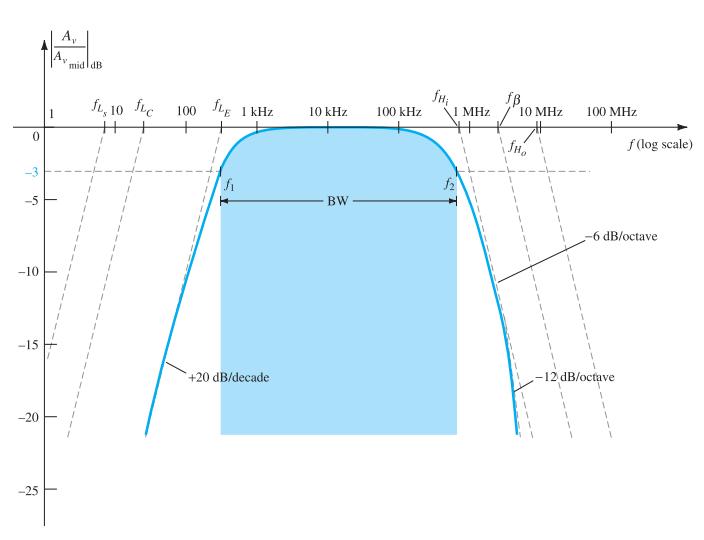
8 Typical Frequency Response The band frequencies define a level where the gain or quantity of interest will be 70.7% of its maximum value. 8


9 Normalized plot Decibel plot Phase plot 9
10 LOW FREQUENCY ANALYSIS- BODE PLOT 10


11 Defining the Low Cutoff Frequency In the low-frequency region of the single-stage BJT or FET amplifier, it is the RC combinations formed by the network capacitors C C, C E, and C s and the network resistive parameters that determine the cutoff frequencies Voltage-Divider Bias Config. 11
12 Bode Plot A change in frequency by a factor of two, equivalent to one octave, results in a 6-dB change in the ratio, as shown by the change in gain from f L /2 to f L. For a 10:1 change in frequency, equivalent to one decade, there is a 20-dB change in the ratio, as demonstrated between the frequencies of f L /10 and f L. The piecewise linear plot of the asymptotes and associated breakpoints is called a Bode plot of the magnitude versus frequency. Phase Angle: 12
13 BJT & JFET AMPLIFIERS LOW FREQUENCY ANALYSIS 13


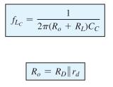
14 Loaded BJT Amplifier In the voltage-divider ct. the capacitors Cs, C C, and C E will determine the low-frequency response. f L = max(f Ls, f Lc, f LE ) Cs: Cc: C E : 14

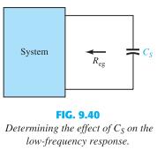
15 Impact of R S 15
16 Example 16


17 FET Amplifier 17
18 MILLER EFFECT 18 J , Lec#7, Nov 2014
 capacitances internal to the active device and the wiring capacitance between leads of the network.")
 capacitance between the input and output terminals of the active")
19 Miller input capacitance In the high-frequency region, the capacitive elements of importance are the interelectrode (between-terminals) capacitances internal to the active device and the wiring capacitance between leads of the network. For any inverting amplifier, the input capacitance will be increased by a Miller effect capacitance sensitive to the gain of the amplifier and the interelectrode (parasitic) capacitance between the input and output terminals of the active device. 19

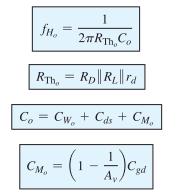
20 Miller output capacitance A positive value for A v would result in a negative capacitance (for Av > 1). For noninverting amplifiers such as the common-base and emitter-follower configurations, the Miller effect capacitance is not a contributing concern for high-frequency applications. The Miller effect will also increase the level of output capacitance, which must also be considered when the high-frequency cutoff is determined. 20
21 BJT & JFET AMPLIFIERS HIGH FREQUENCY RESPONSE 21
22 High Frequency Response At the high-frequency end, there are two factors that define the 3-dB cutoff point: 1. the network capacitance (parasitic and introduced) 2. the frequency dependence of h fe (β). For RC circuit: 22


23 1. Network Parameters : At high frequencies, the various parasitic capacitances (C be, C bc, C ce ) of the transistor are included with the wiring capacitances (C Wi, C Wo ). 23

24 2. h fe (or β) Variation The variation of h fe (or β) with frequency approaches the following relationship: The quantity, f β, is determined by a set of parameters employed in the hybrid π model f β is a function of the bias configuration. the small change in h fb for the chosen frequency range, revealing that the common-base configuration displays improved high-frequency characteristics over the common-emitter configuration. 24

25 Example J , Lec#7, Nov
26 Gain-Bandwidth Product There is a Figure of Merit applied to amplifiers called the Gain-Bandwidth Product (GBP) that is commonly used to initiate the design process of an amplifier. It provides important information about the relationship between the gain of the amplifier and the expected operating frequency range. at any level of gain the product of the two remains a constant. the frequency f T is called the unity-gain frequency and is always equal to the product of the midband gain of an amplifier and the bandwidth at any level of gain. 26

27 FET Amplifier 27
28 For more details, refer to: Chapter 9, Electronic Devices and Circuits, Boylestad. The lecture is available online at: For inquires, send to: 28
Lecture #4 BJT AC Analysis
 November 2014 Ahmad El-Banna Integrated Technical Education Cluster At AlAmeeria J-601-1448 Electronic Principals Lecture #4 BJT AC Analysis Instructor: Dr. Ahmad El-Banna Agenda BJT transistor Modeling
Lecture #3 BJT Transistors & DC Biasing
 November 2014 Ahmad El-Banna Integrated Technical Education Cluster At AlAmeeria J-601-1448 Electronic Principals Lecture #3 BJT Transistors & DC Biasing Instructor: Dr. Ahmad El-Banna Agenda Transistor
BJT & FET Frequency Response
 Chapter 4 BJT & FET Spring 2012 4 th Semester Mechatronics SZABIST, Karachi 2 Course Support humera.rafique@szabist.edu.pk Office: 100 Campus (404) Official: ZABdesk Subsidiary: https://sites.google.com/site/zabistmechatronics/home/spring-2012/ecd
Lecture #9 Tuned Amplifiers
 December 2014 Ahmad El-Banna Integrated Technical Education Cluster At AlAmeeria J-601-1448 Electronic Principals Lecture #9 Tuned Amplifiers Instructor: Dr. Ahmad El-Banna Agenda Class C vs. Tuned Amplifier
Midterm 2 Exam. Max: 90 Points
 Midterm 2 Exam Name: Max: 90 Points Question 1 Consider the circuit below. The duty cycle and frequency of the 555 astable is 55% and 5 khz respectively. (a) Determine a value for so that the average current
Lecture #3 ( 2 weeks) Transistors
 Transistors") Spring 2015 Benha University Faculty of Engineering at Shoubra ECE-291 Electronic Engineering Lecture #3 ( 2 weeks) Transistors Instructor: Dr. Ahmad El-Banna 1 Agenda BJT Structure Basic Operation Transistor
Spring 2015 Benha University Faculty of Engineering at Shoubra ECE-291 Electronic Engineering Lecture #3 ( 2 weeks) Transistors Instructor: Dr. Ahmad El-Banna 1 Agenda BJT Structure Basic Operation Transistor
Homework Assignment 12
 Homework Assignment 12 Question 1 Shown the is Bode plot of the magnitude of the gain transfer function of a constant GBP amplifier. By how much will the amplifier delay a sine wave with the following
ESE319 Introduction to Microelectronics High Frequency BJT Model & Cascode BJT Amplifier
 High Frequency BJT Model & Cascode BJT Amplifier 1 Gain of 10 Amplifier Non-ideal Transistor C in R 1 V CC R 2 v s Gain starts dropping at > 1MHz. Why! Because of internal transistor capacitances that
ECE 255, Discrete-Circuit Amplifiers
 ECE 255, Discrete-Circuit Amplifiers 20 March 2018 In this lecture, we will continue with the study of transistor amplifiers with the presence of biasing circuits and coupling capacitors in place. We will
ESE 372 / Spring 2011 / Lecture 19 Common Base Biased by current source
 ESE 372 / Spring 2011 / Lecture 19 Common Base Biased by current source Output from Collector Start with bias DC analysis make sure BJT is in FA, then calculate small signal parameters for AC analysis.
Last time: BJT CE and CB amplifiers biased by current source
 Last time: BJT CE and CB amplifiers biased by current source Assume FA regime, then VB VC V E I B I E, β 1 I Q C α I, V 0. 7V Calculate V CE and confirm it is > 0.2-0.3V, then BJT can be replaced with
Lecture #2 Operational Amplifiers
 Spring 2015 Benha University Faculty of Engineering at Shoubra ECE-322 Electronic Circuits (B) Lecture #2 Operational Amplifiers Instructor: Dr. Ahmad El-Banna Agenda Introduction Op-Amps Input Modes and
Homework Assignment 11
 Homework Assignment 11 Question 1 (Short Takes) Two points each unless otherwise indicated. 1. What is the 3-dB bandwidth of the amplifier shown below if r π = 2.5K, r o = 100K, g m = 40 ms, and C L =
EC2205 Electronic Circuits-1 UNIT III FREQUENCY RESPONSE OF AMPLIFIERS
 EC2205 Electronic Circuits-1 UNIT III FREQUENCY RESPONSE OF AMPLIFIERS PART A (2 MARK QUESTIONS) 1. Two amplifiers having gain 20 db and 40 db are cascaded. Find the overall gain in db. (NOV/DEC 2009)
Lecture # 12 Oscillators (LC Circuits)
") December 2014 Benha University Faculty of Engineering at Shoubra ECE-312 Electronic Circuits (A) Lecture # 12 Oscillators (LC Circuits) Instructor: Dr. Ahmad El-Banna Agenda The Colpitts Oscillator The
December 2014 Benha University Faculty of Engineering at Shoubra ECE-312 Electronic Circuits (A) Lecture # 12 Oscillators (LC Circuits) Instructor: Dr. Ahmad El-Banna Agenda The Colpitts Oscillator The
UNIT I BIASING OF DISCRETE BJT AND MOSFET PART A
 UNIT I BIASING OF DISCRETE BJT AND MOSFET PART A 1. Why do we choose Q point at the center of the load line? 2. Name the two techniques used in the stability of the q point.explain. 3. Give the expression
ELC224 Final Review (12/10/2009) Name:
 Name:") ELC224 Final Review (12/10/2009) Name: Select the correct answer to the problems 1 through 20. 1. A common-emitter amplifier that uses direct coupling is an example of a dc amplifier. 2. The frequency
ELC224 Final Review (12/10/2009) Name: Select the correct answer to the problems 1 through 20. 1. A common-emitter amplifier that uses direct coupling is an example of a dc amplifier. 2. The frequency
EXP8: AMPLIFIERS II.
 EXP8: AMPLIFIES II. Objectives. The objectives of this lab are:. To analyze the behavior of a class A amplifier. 2. To understand the role the components play in the gain of the circuit. 3. To find the
Lecture #4 Basic Op-Amp Circuits
 Summer 2015 Ahmad El-Banna Faculty of Engineering Department of Electronics and Communications GEE336 Electronic Circuits II Lecture #4 Basic Op-Amp Circuits Instructor: Dr. Ahmad El-Banna Agenda Some
Electron Devices and Circuits
 Electron Devices and Circuits (EC 8353) Prepared by Mr.R.Suresh, AP/EEE Ms.S.KARKUZHALI,A.P/EEE BJT small signal model Analysis of CE, CB, CC amplifiers- Gain and frequency response MOSFET small signal
Tutorial 2 BJTs, Transistor Bias Circuits, BJT Amplifiers FETs and FETs Amplifiers. Part 1: BJTs, Transistor Bias Circuits and BJT Amplifiers
 Tutorial 2 BJTs, Transistor Bias Circuits, BJT Amplifiers FETs and FETs Amplifiers Part 1: BJTs, Transistor Bias Circuits and BJT Amplifiers 1. Explain the purpose of a thin, lightly doped base region.
EC1203: ELECTRONICS CIRCUITS-I UNIT-I TRANSISTOR BIASING PART-A
 SHRI ANGALAMMAN COLLEGE OF ENGG & TECH., TRICHY 621105 (Approved by AICTE, New Delhi and Affiliated to Anna University Chennai/Trichy) ( ISO 9001:2008 Certified Institution) DEPARTMENT OF ELECTRONICS &
G.PULLAIAH COLLEGE OF ENGINEERING & TECHNOLOGY II B.Tech II-SEM MID -I EXAM Branch: EEE Sub: Analog Electronic Circuits Date:
 G.PULLAIAH COLLEGE OF ENGINEERING & TECHNOLOGY II B.Tech II-SEM MID -I EXAM Branch: EEE Sub: Analog Electronic Circuits Date: 08-03-18 Time: 20 minutes Max.Marks:10 1. The amplifier that gives unity current
5.25Chapter V Problem Set
 5.25Chapter V Problem Set P5.1 Analyze the circuits in Fig. P5.1 and determine the base, collector, and emitter currents of the BJTs as well as the voltages at the base, collector, and emitter terminals.
Electronic Devices. Floyd. Chapter 6. Ninth Edition. Electronic Devices, 9th edition Thomas L. Floyd
 Electronic Devices Ninth Edition Floyd Chapter 6 Agenda BJT AC Analysis Linear Amplifier AC Load Line Transistor AC Model Common Emitter Amplifier Common Collector Amplifier Common Base Amplifier Special
CHAPTER.4 :TRANSISTOR FREQUENCY RESPONSE
 CHAPTER.4 :TRANSISTOR FREQUENCY RESPONSE To understand Decibels, log scale, general frequency considerations of an amplifier. low frequency analysis - Bode plot low frequency response BJT amplifier Miller
EXPERIMENT 1: LOW AND HIGH FREQUENCY REGION ANALYSIS OF BJT AMPLIFIERS
 EXPERIMENT 1: LOW AND HIGH FREQUENCY REGION ANALYSIS OF BJT AMPLIFIERS Objective: In single layer common emitter amplifiers, observation of frequency dependence. Materials Transistor: 1x BC237 transistor
Assist Lecturer: Marwa Maki. Active Filters
 Active Filters In past lecture we noticed that the main disadvantage of Passive Filters is that the amplitude of the output signals is less than that of the input signals, i.e., the gain is never greater
Exam Write down one phrase/sentence that describes the purpose of the diodes and constant current source in the amplifier below.
 Exam 3 Name: Score /94 Question 1 Short Takes 1 point each unless noted otherwise. 1. Write down one phrase/sentence that describes the purpose of the diodes and constant current source in the amplifier
BJT Circuits (MCQs of Moderate Complexity)
") BJT Circuits (MCQs of Moderate Complexity) 1. The current ib through base of a silicon npn transistor is 1+0.1 cos (1000πt) ma. At 300K, the rπ in the small signal model of the transistor is i b B C r
BJT Circuits (MCQs of Moderate Complexity) 1. The current ib through base of a silicon npn transistor is 1+0.1 cos (1000πt) ma. At 300K, the rπ in the small signal model of the transistor is i b B C r
Code No: R Set No. 1
 Code No: R059210404 Set No. 1 II B.Tech I Semester Supplimentary Examinations, February 2008 ELECTRONIC CIRCUIT ANALYSIS ( Common to Electronics & Communication Engineering and Electronics & Telematics)
Single-Stage BJT Amplifiers and BJT High-Frequency Model. Single-Stage BJT Amplifier Configurations
 1 Single-Stage BJT Amplifiers and BJT High-Frequency Model Asst. Prof. MONTREE SIRIPRUCHYANUN, D. Eng. Dept. of Teacher Training in Electrical Engineering, Faculty of Technical Education King Mongkut s
 Pg: 1 VALLIAMMAI ENGINEERING COLLEGE SRM Nagar, Kattankulathur 603 203 Department of Electronics & Communication Engineering Regulation: 2013 Acadamic Year : 2015 2016 EC6304 Electronic Circuits I Question
Chapter 6. BJT Amplifiers
 Basic Electronic Devices and Circuits EE 111 Electrical Engineering Majmaah University 2 nd Semester 1432/1433 H Chapter 6 BJT Amplifiers 1 Introduction The things you learned about biasing a transistor
Electronic Circuits for Mechatronics ELCT 609 Lecture 5: BJT Voltage Amplifiers
 Electronic Circuits for Mechatronics ELCT 609 Lecture 5: BJT Voltage Amplifiers Assistant Professor Office: C3.315 E-mail: eman.azab@guc.edu.eg 1 BJT Modes of Operation Electrical Equations of BJT 2 BJT
SIDDHARTH GROUP OF INSTITUTIONS :: PUTTUR (AUTONOMOUS) Siddharth Nagar, Narayanavanam Road QUESTION BANK
 Siddharth Nagar, Narayanavanam Road QUESTION BANK") SIDDHARTH GROUP OF INSTITUTIONS :: PUTTUR (AUTONOMOUS) Siddharth Nagar, Narayanavanam Road 517583 QUESTION BANK Subject with Code : Electronic Circuit Analysis (16EC407) Year & Sem: II-B.Tech & II-Sem
SIDDHARTH GROUP OF INSTITUTIONS :: PUTTUR (AUTONOMOUS) Siddharth Nagar, Narayanavanam Road 517583 QUESTION BANK Subject with Code : Electronic Circuit Analysis (16EC407) Year & Sem: II-B.Tech & II-Sem
UNIVERSITY OF NORTH CAROLINA AT CHARLOTTE Department of Electrical and Computer Engineering
 UNIVERSITY OF NORTH CAROLINA AT CHARLOTTE Department of Electrical and Computer Engineering EXPERIMENT 7 BJT AMPLIFIER CONFIGURATIONS AND INPUT/OUTPUT IMPEDANCE OBJECTIVES The purpose of this experiment
Basic electronics Prof. T.S. Natarajan Department of Physics Indian Institute of Technology, Madras Lecture- 17. Frequency Analysis
 Basic electronics Prof. T.S. Natarajan Department of Physics Indian Institute of Technology, Madras Lecture- 17 Frequency Analysis Hello everybody! In our series of lectures on basic electronics learning
Phy 335, Unit 4 Transistors and transistor circuits (part one)
") Mini-lecture topics (multiple lectures): Phy 335, Unit 4 Transistors and transistor circuits (part one) p-n junctions re-visited How does a bipolar transistor works; analogy with a valve Basic circuit
Mini-lecture topics (multiple lectures): Phy 335, Unit 4 Transistors and transistor circuits (part one) p-n junctions re-visited How does a bipolar transistor works; analogy with a valve Basic circuit
Radio Frequency Electronics
 Radio Frequency Electronics Active Components IV Samuel Morse Born in 79 in Massachusetts Fairly accomplished painter After witnessing various electrical experiments, got intrigued by electricity Designed
Unit- I- Biasing Of Discrete BJT and MOSFET
 Part- A QUESTIONS: Unit- I- Biasing Of Discrete BJT and MOSFET 1. Describe about BJT? BJT consists of 2 PN junctions. It has three terminals: emitter, base and collector. Transistor can be operated in
II/IV B. TECH. DEGREE EXAMINATIONS, NOVEMBER Second Semester EC/EE ELECTRONIC CIRCUIT ANALYSIS. Time : Three Hours Max.
 Total No. of Questions : 9] [Total No. of Pages : 02 B.Tech. II/ IV YEAR DEGREE EXAMINATION, APRIL/MAY - 2014 (Second Semester) EC/EE/EI Electronic Circuit Analysis Time : 03 Hours Maximum Marks : 70 Q1)
Small signal ac equivalent circuit of BJT
 UNIT-2 Part A 1. What is an ac load line? [N/D 16] A dc load line gives the relationship between the q-point and the transistor characteristics. When capacitors are included in a CE transistor circuit,
Homework Assignment 05
 Homework Assignment 05 Question (2 points each unless otherwise indicated)(20 points). Estimate the parallel parasitic capacitance of a mh inductor with an SRF of 220 khz. Answer: (2π)(220 0 3 ) = ( 0
Differential Amplifier Design
 Differential Amplifier Design Design with ideal current source bias. Differential and common mode gain results Add finite output resistance to current source. Replace ideal current source with current
Electronics Prof. D. C. Dube Department of Physics Indian Institute of Technology, Delhi
 Electronics Prof. D. C. Dube Department of Physics Indian Institute of Technology, Delhi Module No # 05 FETS and MOSFETS Lecture No # 06 FET/MOSFET Amplifiers and their Analysis In the previous lecture
Analog and Telecommunication Electronics
 Politecnico di Torino - ICT School Analog and Telecommunication Electronics A3 BJT Amplifiers»Biasing» Output dynamic range» Small signal analysis» Voltage gain» Frequency response 12/03/2012-1 ATLCE -
Lecture #1 Course Introduction and Amplifier Feedback Concepts
 Summer 2015 Ahmad El-Banna Faculty of Engineering Department of Electronics and Communications GEE336 Electronic Circuits II Lecture #1 Course Introduction and Amplifier Feedback Concepts Instructor: Dr.
(b) 25% (b) increases
 25% (b) increases") Homework Assignment 07 Question 1 (2 points each unless noted otherwise) 1. In the circuit 10 V, 10, and 5K. What current flows through? Answer: By op-amp action the voltage across is and the current through
Homework Assignment 07 Question 1 (2 points each unless noted otherwise) 1. In the circuit 10 V, 10, and 5K. What current flows through? Answer: By op-amp action the voltage across is and the current through
Amplifier Frequency Response, Feedback, Oscillations; Op-Amp Block Diagram and Gain-Bandwidth Product
 Amplifier Frequency Response, Feedback, Oscillations; Op-Amp Block Diagram and Gain-Bandwidth Product Physics116A,12/4/06 Draft Rev. 1, 12/12/06 D. Pellett 2 Negative Feedback and Voltage Amplifier AB
Homework Assignment 06
 Homework Assignment 06 Question 1 (Short Takes) One point each unless otherwise indicated. 1. Consider the current mirror below, and neglect base currents. What is? Answer: 2. In the current mirrors below,
ATLCE - A3 01/03/2016. Analog and Telecommunication Electronics 2016 DDC 1. Politecnico di Torino - ICT School. Lesson A3: BJT Amplifiers
 Politecnico di Torino - ICT School Analog and Telecommunication Electronics A3 BJT Amplifiers»Biasing» Output dynamic range» Small signal analysis» ltage gain» Frequency response AY 2015-16 Biasing Output
The Miller Approximation. CE Frequency Response. The exact analysis is worked out on pp of H&S.
 CE Frequency Response The exact analysis is worked out on pp. 639-64 of H&S. The Miller Approximation Therefore, we consider the effect of C µ on the input node only V ---------- out V s = r g π m ------------------
Mini Project 2 Single Transistor Amplifiers. ELEC 301 University of British Columbia
 Mini Project 2 Single Transistor Amplifiers ELEC 301 University of British Columbia 44638154 October 27, 2017 Contents 1 Introduction 1 2 Investigation 1 2.1 Part 1.................................................
DHANALAKSHMI COLLEGE OF ENGINEERING DEPARTMENT OF ELECTRICAL AND ELECTRONICS ENGINEERING EC6202 ELECTRONIC DEVICES AND CIRCUITS
 DHANALAKSHMI COLLEGE OF ENGINEERING DEPARTMENT OF ELECTRICAL AND ELECTRONICS ENGINEERING EC6202 ELECTRONIC DEVICES AND CIRCUITS UNIT-I - PN DIODEAND ITSAPPLICATIONS 1. What is depletion region in PN junction?
ECE 255, MOSFET Amplifiers
 ECE 255, MOSFET Amplifiers 26 October 2017 In this lecture, the basic configurations of MOSFET amplifiers will be studied similar to that of BJT. Previously, it has been shown that with the transistor
UNIT I PN JUNCTION DEVICES
 UNIT I PN JUNCTION DEVICES 1. Define Semiconductor. 2. Classify Semiconductors. 3. Define Hole Current. 4. Define Knee voltage of a Diode. 5. What is Peak Inverse Voltage? 6. Define Depletion Region in
Lecture #1 Course Introduction and Differential Amplifiers
 Spring 2015 Benha University Faculty of Engineering at Shoubra ECE-322 Electronic Circuits (B) Lecture #1 Course Introduction and Differential Amplifiers Instructor: Dr. Ahmad El-Banna Agenda Course Objectives
Electronic Circuits ELCT604 (Spring 2018) Lecture 2 BJT Amplifiers
 Lecture 2 BJT Amplifiers") Electronic Circuits ELCT604 (Spring 2018) Lecture 2 BJT Amplifiers Assistant Professor Office: C3.315 E-mail: eman.azab@guc.edu.eg 1 Analog Voltage Amplifiers Circuit Design and Configurations 2 Objective
Electronic Circuits ELCT604 (Spring 2018) Lecture 2 BJT Amplifiers Assistant Professor Office: C3.315 E-mail: eman.azab@guc.edu.eg 1 Analog Voltage Amplifiers Circuit Design and Configurations 2 Objective
Page 1. Telecommunication Electronics ETLCE - A2 06/09/ DDC 1. Politecnico di Torino ICT School. Amplifiers
 Politecnico di Torino ICT School Amplifiers Telecommunication Electronics A2 Transistor amplifiers» Bias point and circuits,» Small signal models» Gain and bandwidth» Limits of linear analysis Op Amp amplifiers
Lab 2: Discrete BJT Op-Amps (Part I)
") Lab 2: Discrete BJT Op-Amps (Part I) This is a three-week laboratory. You are required to write only one lab report for all parts of this experiment. 1.0. INTRODUCTION In this lab, we will introduce and
Lab 2: Discrete BJT Op-Amps (Part I) This is a three-week laboratory. You are required to write only one lab report for all parts of this experiment. 1.0. INTRODUCTION In this lab, we will introduce and
Mini Project 3 Multi-Transistor Amplifiers. ELEC 301 University of British Columbia
 Mini Project 3 Multi-Transistor Amplifiers ELEC 30 University of British Columbia 4463854 November 0, 207 Contents 0 Introduction Part : Cascode Amplifier. A - DC Operating Point.......................................
Electronics EECE2412 Spring 2018 Exam #2
 Electronics EECE2412 Spring 2018 Exam #2 Prof. Charles A. DiMarzio Department of Electrical and Computer Engineering Northeastern University 29 March 2018 File:12262/exams/exam2 Name: General Rules: You
Experiment 8 Frequency Response
 Experiment 8 Frequency Response W.T. Yeung, R.A. Cortina, and R.T. Howe UC Berkeley EE 105 Spring 2005 1.0 Objective This lab will introduce the student to frequency response of circuits. The student will
EXPT NO: 1.A. COMMON EMITTER AMPLIFIER (Software) PRELAB:
 PRELAB:") EXPT NO: 1.A COMMON EMITTER AMPLIFIER (Software) PRELAB: 1. Study the operation and working principle of CE amplifier. 2. Identify all the formulae you will need in this Lab. 3. Study the procedure of
EXPT NO: 1.A COMMON EMITTER AMPLIFIER (Software) PRELAB: 1. Study the operation and working principle of CE amplifier. 2. Identify all the formulae you will need in this Lab. 3. Study the procedure of
Lecture 33: Context. Prof. J. S. Smith
 Lecture 33: Prof J. S. Smith Context We are continuing to review some of the building blocks for multi-stage amplifiers, including current sources and cascode connected devices, and we will also look at
PHYSICS 330 LAB Operational Amplifier Frequency Response
 PHYSICS 330 LAB Operational Amplifier Frequency Response Objectives: To measure and plot the frequency response of an operational amplifier circuit. History: Operational amplifiers are among the most widely
55:041 Electronic Circuits The University of Iowa Fall Exam 3. Question 1 Unless stated otherwise, each question below is 1 point.
 Exam 3 Name: Score /65 Question 1 Unless stated otherwise, each question below is 1 point. 1. An engineer designs a class-ab amplifier to deliver 2 W (sinusoidal) signal power to an resistive load. Ignoring
Module-1 BJT AC Analysis: The re Transistor Model. Common-Base Configuration
 Module-1 BJT AC Analysis: BJT AC Analysis: BJT AC Analysis: BJT Transistor Modeling, The re transistor model, Common emitter fixed bias, Voltage divider bias, Emitter follower configuration. Darlington
Homework Assignment 07
 Homework Assignment 07 Question 1 (Short Takes). 2 points each unless otherwise noted. 1. A single-pole op-amp has an open-loop low-frequency gain of A = 10 5 and an open loop, 3-dB frequency of 4 Hz.
 VALLIAMMAI ENGINEERING COLLEGE SRM NAGAR, KATTANKULATHUR- 603 203 DEPARTMENT OF ELECTRONICS AND COMMUNICATION ENGINEERING EC6202- ELECTRONIC DEVICES AND CIRCUITS UNIT I PN JUNCTION DEVICES 1. Define Semiconductor.
ECE 310L : LAB 9. Fall 2012 (Hay)
") ECE 310L : LAB 9 PRELAB ASSIGNMENT: Read the lab assignment in its entirety. 1. For the circuit shown in Figure 3, compute a value for R1 that will result in a 1N5230B zener diode current of approximately
ECE 310L : LAB 9 PRELAB ASSIGNMENT: Read the lab assignment in its entirety. 1. For the circuit shown in Figure 3, compute a value for R1 that will result in a 1N5230B zener diode current of approximately
School of Sciences. ELECTRONICS II ECE212A 2 nd Assignment
 School of Sciences SPRING SEMESTER 2010 INSTRUCTOR: Dr Konstantinos Katzis COURSE / SECTION: ECE212N COURSE TITLE: Electronics II OFFICE RM#: 124 (1 st floor) OFFICE TEL#: 22713296 OFFICE HOURS: Monday
Lab 4 : Transistor Oscillators
 Objective: Lab 4 : Transistor Oscillators In this lab, you will learn how to design and implement a colpitts oscillator. In part II you will implement a RC phase shift oscillator Hardware Required : Pre
Microelectronic Circuits - Fifth Edition Sedra/Smith Copyright 2004 by Oxford University Press, Inc.
 Feedback 1 Figure 8.1 General structure of the feedback amplifier. This is a signal-flow diagram, and the quantities x represent either voltage or current signals. 2 Figure E8.1 3 Figure 8.2 Illustrating
GATE: Electronics MCQs (Practice Test 1 of 13)
") GATE: Electronics MCQs (Practice Test 1 of 13) 1. Removing bypass capacitor across the emitter leg resistor in a CE amplifier causes a. increase in current gain b. decrease in current gain c. increase
GATE: Electronics MCQs (Practice Test 1 of 13) 1. Removing bypass capacitor across the emitter leg resistor in a CE amplifier causes a. increase in current gain b. decrease in current gain c. increase
15EEE282 Electronic Circuits and Simulation Lab - I Lab # 6
 Exp. No #6 FREQUENCY RESPONSE OF COMMON EMITTER AMPLIFIER OBJECTIVE The purpose of the experiment is to design a common emitter amplifier. To analyze and plot the frequency response of the amplifier with
ECE 2201 PRELAB 6 BJT COMMON EMITTER (CE) AMPLIFIER
 AMPLIFIER") ECE 2201 PRELAB 6 BJT COMMON EMITTER (CE) AMPLIFIER Hand Analysis P1. Determine the DC bias for the BJT Common Emitter Amplifier circuit of Figure 61 (in this lab) including the voltages V B, V C and V
ECE 2201 PRELAB 6 BJT COMMON EMITTER (CE) AMPLIFIER Hand Analysis P1. Determine the DC bias for the BJT Common Emitter Amplifier circuit of Figure 61 (in this lab) including the voltages V B, V C and V
Reading. Lecture 33: Context. Lecture Outline. Chapter 9, multi-stage amplifiers. Prof. J. S. Smith
 eading Lecture 33: Chapter 9, multi-stage amplifiers Prof J. S. Smith Context Lecture Outline We are continuing to review some of the building blocks for multi-stage amplifiers, including current sources
Unit WorkBook 4 Level 4 ENG U19 Electrical and Electronic Principles LO4 Digital & Analogue Electronics 2018 Unicourse Ltd. All Rights Reserved.
 Pearson BTEC Levels 4 Higher Nationals in Engineering (RQF) Unit 19: Electrical and Electronic Principles Unit Workbook 4 in a series of 4 for this unit Learning Outcome 4 Digital & Analogue Electronics
Lecture #4 Special-purpose Op-amp Circuits
 Spring 2015 Benha University Faculty of Engineering at Shoubra ECE-322 Electronic Circuits (B) Lecture #4 Special-purpose Op-amp Circuits Instructor: Dr. Ahmad El-Banna Agenda Instrumentation Amplifiers
Linear electronic. Lecture No. 1
 1 Lecture No. 1 2 3 4 5 Lecture No. 2 6 7 8 9 10 11 Lecture No. 3 12 13 14 Lecture No. 4 Example: find Frequency response analysis for the circuit shown in figure below. Where R S =4kR B1 =8kR B2 =4k R
The George Washington University School of Engineering and Applied Science Department of Electrical and Computer Engineering ECE 20 - LAB
 The George Washington University School of Engineering and Applied Science Department of Electrical and Computer Engineering ECE 20 - LAB Experiment # 6 (Part I) Bipolar Junction Transistors Common Emitter
Federal Urdu University of Arts, Science & Technology Islamabad Pakistan THIRD SEMESTER ELECTRONICS - II BASIC ELECTRICAL & ELECTRONICS LAB
 THIRD SEMESTER ELECTRONICS - II BASIC ELECTRICAL & ELECTRONICS LAB DEPARTMENT OF ELECTRICAL ENGINEERING Prepared By: Checked By: Approved By: Engr. Saqib Riaz Engr. M.Nasim Khan Dr.Noman Jafri Lecturer
ECE 334: Electronic Circuits Lecture 2: BJT Large Signal Model
 Faculty of Engineering ECE 334: Electronic Circuits Lecture 2: BJT Large Signal Model Agenda I & V Notations BJT Devices & Symbols BJT Large Signal Model 2 I, V Notations (1) It is critical to understand
CHAPTER 11. Feedback. Microelectronic Circuits, Seventh Edition. Copyright 2015 by Oxford University Press
 CHAPTER 11 Feedback Figure 11.1 General structure of the feedback amplifier. This is a signal-flow diagram, and the quantities x represent either voltage or current signals. Figure 11.2 Determining the
ECE 255, MOSFET Basic Configurations
 ECE 255, MOSFET Basic Configurations 8 March 2018 In this lecture, we will go back to Section 7.3, and the basic configurations of MOSFET amplifiers will be studied similar to that of BJT. Previously,
Frequency Response of Common Emitter Amplifier
 Başkent University Department of Electrical and Electronics Engineering EEM 311 Electronics II Experiment 6 Frequency Response of Common Emitter Amplifier Aim: The aim of this experiment is to study the
CLASS 5 BJT CONFIGURATIONS AND I V CHARACTERISTICS
 CLASS 5 BJT CONFIGURATIONS AND I V CHARACTERISTICS CE is the most typical configuration used. For this configuration, the voltage gain, A v =V out /V i,ishigh.ahigha v means the amplifier is efficient.
Single-Stage Integrated- Circuit Amplifiers
 Single-Stage Integrated- Circuit Amplifiers Outline Comparison between the MOS and the BJT From discrete circuit to integrated circuit - Philosophy, Biasing, etc. Frequency response The Common-Source and
Department of Electrical Engineering and Computer Sciences, University of California
 Chapter 8 NOISE, GAIN AND BANDWIDTH IN ANALOG DESIGN Robert G. Meyer Department of Electrical Engineering and Computer Sciences, University of California Trade-offs between noise, gain and bandwidth are
Small Signal Amplifiers - BJT. Definitions Small Signal Amplifiers Dimensioning of capacitors
 Small Signal mplifiers BJT Defitions Small Signal mplifiers Dimensiong of capacitors 1 Defitions (1) Small signal condition When the put signal (v and, i ) is small so that output signal (v out and, i
Operational Amplifier BME 360 Lecture Notes Ying Sun
 Operational Amplifier BME 360 Lecture Notes Ying Sun Characteristics of Op-Amp An operational amplifier (op-amp) is an analog integrated circuit that consists of several stages of transistor amplification
Document Name: Electronic Circuits Lab. Facebook: Twitter:
 Document Name: Electronic Circuits Lab www.vidyathiplus.in Facebook: www.facebook.com/vidyarthiplus Twitter: www.twitter.com/vidyarthiplus Copyright 2011-2015 Vidyarthiplus.in (VP Group) Page 1 CIRCUIT
SAMPLE FINAL EXAMINATION FALL TERM
 ENGINEERING SCIENCES 154 ELECTRONIC DEVICES AND CIRCUITS SAMPLE FINAL EXAMINATION FALL TERM 2001-2002 NAME Some Possible Solutions a. Please answer all of the questions in the spaces provided. If you need
Experiments #6. Differential Amplifier
 Experiments #6 Differential Amplifier 1) Objectives: To understand the DC and AC operation of a differential amplifier. To measure DC voltages and currents in differential amplifier. To obtain measured
FREQUENTLY ASKED QUESTIONS
 FREQUENTLY ASKED QUESTIONS UNIT-1 SUBJECT : ELECTRONIC DEVICES AND CIRCUITS SUBJECT CODE : EC6202 BRANCH: EEE PART -A 1. What is meant by diffusion current in a semi conductor? (APR/MAY 2010, 2011, NOV/DEC
dc Bias Point Calculations
 dc Bias Point Calculations Find all of the node voltages assuming infinite current gains 9V 9V 10kΩ 9V 100kΩ 1kΩ β = 270kΩ 10kΩ β = 1kΩ 1 dc Bias Point Calculations Find all of the node voltages assuming
EK307 Passive Filters and Steady State Frequency Response
 EK307 Passive Filters and Steady State Frequency Response Laboratory Goal: To explore the properties of passive signal-processing filters Learning Objectives: Passive filters, Frequency domain, Bode plots
Early Effect & BJT Biasing
 Early Effect & BJT Biasing Early Effect DC BJT Behavior DC Biasing the BJT 1 ESE319 Introduction to Microelectronics Early Effect Saturation region Forward-Active region 4 3 Ideal NPN BJT Transfer V Characteristic