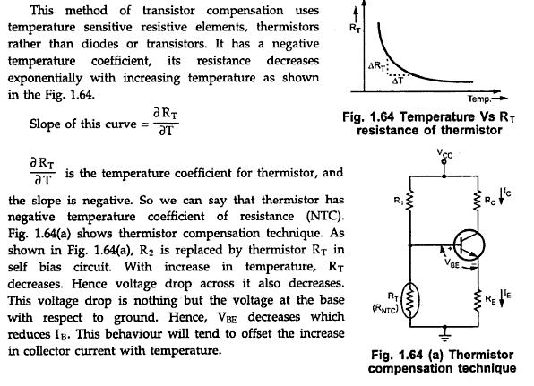
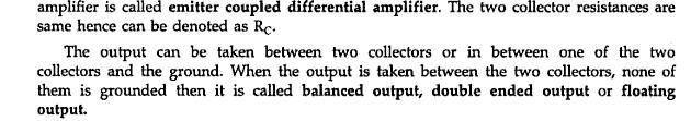
UNIVERSITY PART-B ANSWERS UNIT-1
|
|
|
- Ellen Fletcher
- 6 years ago
- Views:
Transcription
1 UNERSTY PART-B ANSWERS UNT-. Discuss about the DC load line and Q point. (OR) What is D.C. load line, how will you select the operating point, explain it using common emitter amplifier characteristics as an example?[no/dec-06,09,,][may/jun-,3] DC load line:- t is the line on the output characteristics of a transistor circuit which gives the values of C and CE corresponding to zero signal (or) DC conditions. The transistor is biased with a common supply such that the base emitter junction is forward biased and the collector base junction is reversed biased, i.e. Transistor is in the active region. n the absence of ac signal, the capacitors provide very high impedance, i.e. open circuit. Therefore, the equivalent circuit for common emitter amplifier because, as shown fig. Applying Kirchhoff s voltage law to the collector circuit shown in fig. We get, CC - C (R C +R E ) CE = 0 CC = C (R C +R E ) + CE Where C (R C +R E ) is the voltage drop across R C and R E, and CE is the collector emitter voltage. f we arrange the
2 terms in equation as C CE R R R R C E C CC E R dc CE R CC dc R R R dc C E And compare this equation with equation of straight line y = mx +c, where m is the slope of the line and c is the intercept on y axis, then we can draw a straight line on the graph of C s CE which is having slope (-/R dc ) & y intercept CC /R dc. To determine the two points on the line we assume CE = CC & CE = 0.. When CE = CC ; C = 0 and we get a point of cut-off. When CE = 0; C = CC /R dc & we get a point saturation region Q point: The term biasing appearing for the application of dc voltages to establish a fixed level of current and voltage. For transistor amplifiers the resulting dc current and voltage establish an operating point on the characteristics that define the region that will be employed for amplification of the applied signal. Since the operating point is a fixed point on the
3 characteristics, it is also called the quiescent point (abbreviated Q-point).The intersection of the two points is called operating point. By definition, quiescent means quiet, still, inactive. The above figure as a general output device characteristic with three operating points indicated. The biasing circuit can be designed to set the device operation at any of these points or others within the active region. Fig shows the horizontal line for the maximum collector current C max and a vertical line at the maximum collector-to-emitter voltage CEmax. At the lower end of the scales are the cutoff region, defined by B 0 µa, and the saturation region, defined by CE CEsat. The BJT device could be biased to operate outside these maximum limits, but the result of such operation would be either a considerable shortening of the lifetime of the device or destruction of the device. Confining ourselves to the active region, one can select many different operating areas or points. Fig. Transistor is driven into active region because the Q point is close to the Active for the driven input signal. 3
4 The chosen Q-point often depends on the intended use of the circuit. biased the BJT at a desired operating point, the effect of temperature must also be taken into account. Temperature causes the device parameters such as the transistor current gain (β) and the transistor leakage current ( CEO ) to change. Higher temperatures result in increased leakage currents in the device, thereby changing the operating condition set by the biasing network. The result is that the network design must also provide a degree of temperature stability so that temperature changes result in minimum changes in the operating point. This maintenance of the operating point can be specified by a stability factor, S, which indicates the degree of change in operating point due to a temperature variation. A highly stable circuit is desirable, and the stability of a few basic bias circuits will be compared. For the BJT to be biased in its linear or active operating region the following must be true:. The base emitter junction must be forward-biased (p-region voltage more positive), with a resulting forward-bias voltage of about 0.6 to The base collector junction must be reverse-biased (n-region more positive), with the reverse-bias voltage being any value within the maximum limits of the device. Region Active-region operation Cutoff-region operation Saturation-region operation Base emitter junction Forward biased Reverse biased Forward biased Base collector junction Reverse biased Reverse biased Forward biased 4
5 . Explain the fixed biasing of BJT with analysis.[may/jun-0] Biasing:- The process of giving proper supply voltages and resistances for obtaining the Q point is called biasing. The fixed biasing is otherwise called as base bias. For the dc analysis the network can be isolated from the indicated ac levels by replacing the capacitors with an open circuit equivalent. n addition, the dc supply CC can be separated into two supplies (for analysis purposes only) as shown in Fig to permit a separation of input and output circuits. t also reduces the linkage between the two to the base current B. The CC is connected directly to R B and R C just as in Fig. Circuit Diagram: Base Circuit: Consider first the base emitter circuit loop :Writing Kirchhoff s voltage equation in the clockwise direction for the loop, we obtain Note the polarity of the voltage drop across R B as established by the indicated direction of B. Solving the equation for the current B will result in the following: 5
6 Equation - is certainly not a difficult one to remember if one simply keeps in mind that the base current is the current through R B and by Ohm s law that current is the voltage across R B divided by the resistance R B. The voltage across R B is the applied voltage CC at one end less the drop across the base-to-emitter junction ( BE ). n addition, since the supply voltage CC and the base emitter voltage BE are constants, the selection of a base resistor, RB, sets the level of base current for the operating point. Collector Circuit: The collector emitter section of the network is the indicated direction of current C and the resulting polarity across RC. The magnitude of the collector current is related directly to B through The base current is controlled by the level of R B and C is related to B by a constant β, the magnitude of C is not a function of the resistance R C. Change R C to any level and it will not affect the level of B or C as long as we remain in the active region of the device. However, as we shall see, the level of R C will determine the magnitude of CE, which is an important parameter. Applying Kirchhoff s voltage law in the clockwise direction around the indicated closed loop of Fig. will result in the following: and which states in words that the voltage across the collector emitter region of a transistor in the fixed-bias configuration is the supply voltage less the drop across R C where CE is the voltage from collector to emitter and C and E are the voltages from collector and emitter to ground respectively. But in this case, since E = 0,we have n addition,since And E =0 6
7 3. Determine the following for the fixed bias configuration of fig. [MAY/JUN-0] (a) BQ and CQ. (c) B and C. (b) CEQ. (d) BC 3. Explain the collector to base biasing of BJT with analysis.[no/dec-09] The fig shows the dc bias with voltage feedback. t is also called the collector to base boas. t is an improvement over the fixed bias method. n this biasing resistor is connected between the collector and base of the transistor to provide a feedback path. Thus B flows through R B and( C + B ) flow through the R C. Circuit Diagram: Circuit Analysis: Base Circuit: Let us consider the base circuit, apply the voltage law to the base circuit we get, CC = (R B +R C ) B + C R C + BE = (R B +R C ) B + β B R C + BE B = CC - BE / R B + β R C β>> 7
8 Collector Circuit: Apply KL to the output circuit CC = ( C + B ) R C + CE CE = CC -( C + B )R C 4. Determine the quiescent levels of CQ and CEQ for the network of Fig. 5. Explain the oltage divider biasing of BJT with analysis.[no/dec -07,] n the previous bias configurations the bias current CQ and voltage CEQ were a function of the current gain (β) of the transistor. However, since β is temperature sensitive, especially for silicon transistors, and the actual value of beta is usually not well defined, it would be desirable to develop a bias circuit that is less dependent, or in fact, independent of the transistor beta f analyzed on an exact basis the sensitivity to changes in betais quite small. f the circuit parameters are properly chosen, the resulting levels of CQ and CEQ can be almost totally independent of beta. Circuit Diagram: Base Circuit: Let us consider base circuit,oltage across base R is the voltage B,Apply KL voltage divider theorem to find the B, we get, 8
9 >> B Collector Circuit: Let us consider collector circuit, voltage across R E ( E ) can be obtained as, Apply KL to the collector circuit, Simplified Circuit of oltage Divider Bias: Her R and R are replaced by R B and T, where R B is the Thevenin s voltage. R B can be calculated as, 6. For the circuit as shown in fig. β =00 for the si transistor. Calculate CE an 9
10 7. For the circuit shown in fig. C =ma, β =00, Calculate R E, EC and stability factor. 0
11 8. 8. Stability factor for a fixed bias circuit. [MAY/JUN-0] [NO/DEC-09]
12 9. Explain about the fixed bias configuration for JFET with analysis. The simplest of biasing arrangements for the n-channel JFET. Referred to as the fixed-bias configuration, it is one of the few FET configurations that can be solved just as directly using either a mathematical or graphical approach. The configuration of Fig. 6. includes the ac levels i and o and the coupling capacitors (C and C). Recall that the coupling capacitors are open circuits for the dc analysis. Circuit Diagram: DC analysis: The zero-volt drop across RG permits replacing RG by a short-circuit equivalent, as appearing in the network.the fact that the negative terminal of the battery is connected directly to the defined positive potential of GS clearly reveals that the polarity of GS is directly opposite to that of GG. Applying Kirchhoff s voltage law, Since GG is a fixed dc supply, the voltage CC is fixed in magnitude, and hence the name fixed circuit. The drain to source voltage of output circuit can be determined by applying KL.
13 The Q point of the JFET amplifier with fixed bias circuit is given by: Since GS is a fixed quantity for this configuration, its magnitude and sign can simply be substituted into Shockley s equation and the resulting level of D calculated. Graphical Analysis: A graphical analysis would require a plot of Shockley s equation as shown in. Recall that choosing GS = P / will result in a drain current of DSS /4 when plotting the equation. For the analysis of this chapter, the three points defined by DSS, P, and the intersection just described will be sufficient for plotting the curve. The fixed level of GS has been superimposed as a vertical line at GS = - GG. At any point on the vertical line, the level of GS is GG the level of D must simply be determined on this vertical line. The point where the two curves intersect is the common solution to the configurationcommonly referred to as the quiescent or operating point. The subscript Q will be applied to drain current and gate-to-source voltage to identify their levels at the Q-point. Note in Fig. that the quiescent level of D is determined by drawing a horizontal line from the Q-point to the vertical D axis as shown in Fig.. The drain-to-source voltage of the output section can be determined by applying Kirchhoff s voltage law as follows 3
14 Determine the following for the network of Fig. (a) GSQ. (b) DQ. (c) DS. (d) D. (e) G. (f) S. Graphical Approach: The resulting Shockley curve and the vertical line at GS=- are provided in above fig. t is certainly difficult to read beyond the second place without significantly in\ 4

15 0. Discuss the various techniques of stabilization of Q-point in a transistor. [NO/DEC- 09] 5
16 6
17 7
18 8
 GS () g m (3) R s.")
19 . The amplifier shown in Fig. an n-channel FET for which, D =0.8mA, P =-0 and DSS =.6mA. Assume that r d >R d. Find () GS () g m (3) R s. [NO/DEC-007] 9
20 UNT- PART-B ANNA UNERSTY QUESTONS ) Compare CB,CE and CC amplifiers [NO/DEC-09,][APR/MAY-0,3] Characteristics Common base Common emitter Common collector nput resistance ery low Low High output resistance ery high High Low nput voltage Emitter and base Base and emitter Base and collector applied between Output voltage Collector and base Collector and Emitter and taken between emitter collector Current amplification factor C E C B E B Current gain Less than unity High High oltage gain Medium Medium low applications As a input stage of For audio signal For impedance multistage amplification matching amplifiers CE Amplifier Circuit CC Amplifier Circuit 0
 oltage gain c) nput impedance d) Output admittance [APR/MAY-0,][NO/DEC-06,] Let us consider transistor amplifier as a black box as")
21 CB Amplifier Circuit ) Derive the expression for the following of a small signal transistor amplifier in terms of the h-parameters, a) Current gain b) oltage gain c) nput impedance d) Output admittance [APR/MAY-0,][NO/DEC-06,] Let us consider transistor amplifier as a black box as shown,
22
23 3
24 Table Summarizing the Equations 4

25 3) Explain The Operation Of Emitter Coupled Differential Amplifier. [APR/MAY-0][NO/DEC-06,09,] The transistorized differential amplifier is also called as emitter coupled differential amplifier. 5
26 6
27 7

28 4) For the CC transistor amplifier circuit, find the expression for input impedance and voltage gain. Assume suitable model for transistor. [ NO/DEC-09] For a common collector model,collector is made as common and output is taken from emitter. the current direction is now exactly opposite that of CE model because the current always points towards emitter. 8
29 5) With mathematical substantiation draw the basic circuit of Darlington pair and explain. [NO/DEC-08] DARLNGTON TRANSSTORS The direct coupling of two stages of emitter follower amplifier and this cascaded connection of two emitter followers is called the Darlington connection. 9
30 30
31 3
32 3
33 33
34 34

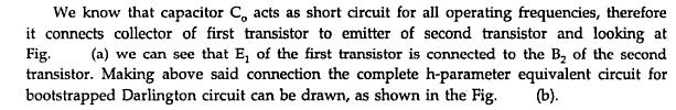
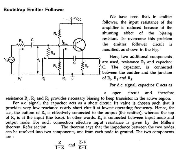
35 6) Explain bootstrapped Darlington circuit with neat sketch [NO/DEC-06] Bootstrapped Darlington Circuit 35

36 n bootstrap emitter follower while eliminating the shunting effect of Rand R there exists a maximum limit on the input resistance. This maximum limit is put by the collector to base resistance of transistor that appears in parallel with input resistance. This is expressed in admittance form by the parameter hob of the transistor. 36
37 37
38 7. Explain the common emitter amplifier. To make the transistor work as an amplifier, it is to be biased to operate in the active region, (i.e.) base emitter junction is to be forward biased, while base collector junction to be reversed biased. Let us consider the common emitter amplifier circuit using self bias or voltage divider bias as shown above. n the absence of input signal, only dc voltages are present in the circuit. This is known as zero-signal or no signal condition or quiescent condition for the amplifier. The dc collector emitter voltage CE, the dc collector current C and dc base current B is the quiescent operating point for the amplifier. On this dc quiescent operating point, we super impose ac signal by application of ac sinusoidal voltage at the input. Due to this base current varies sinusoidally as show in fig. The output current i.e. the collector current is times larger than the input base current in common emitter configuration. Hence the collector current will also vary sinusoidally about its quiescent value, CQ. The output voltage will also vary sinusoidally as shown below. 38
39 The variations in the collector current and the voltage between collector and emitter due to change in the base current are shown below with the help of load line. The collector current varies above and below its Q point value in-phase with the base current and the collector to emitter voltage varies above and below its Q point value 80 out of, phase with the base voltage. When one cycle of input is completed, one cycle of output will also be completed. This means the frequency of output sinusoidal is the same as the frequency of input sinusoid. 39
40 8. Explain the practical common emitter amplifier circuit. follows. t consists of different circuit component. The functions of these components are as Biasing circuit The resistances R, R and RE form the voltage divider biasing circuit for the CE amplifier. t sets the proper operating point for the CE amplifier. Function of nput capacitor C in CE amplifier circuit This capacitor couples the signal to the base of the transistor. t blocks any dc component present in the signal and passes only ac signal for amplification. Need for emitter bypass capacitor CE is used in CE amplifier circuit An emitter bypass capacitor CE is connected in parallel with the emitter resistance RE to provide a low reactance path to the amplified ac signal. f it is not inserted, the amplified ac signal passing through RE will cause a voltage drop across it. This will reduce the output voltage, reducing the gain of the amplifier. Need for output coupling capacitor C The coupling capacitor C couples the output of the amplifier to the load or to the next stage of the amplifier. t blocks dc and passes only ac part of the amplified signal. Need for C, C and CE 40
41 We know that the impedance of capacitor is given as, Xc = f c Thus, at signal frequencies, all the capacitors have extremely small impedance and it can be treated as an ac short circuit. For bias / dc conditions of the transistor all the capacitors act as a dc open circuit. Consider that the signal source is connected directly to the base of the transistor as shown below. The source resistance Rs is in parallel with R and this will reduce the bias voltage at the transistor base and consequently alter the collector current, which is not desired. By connecting RL directly, the dc levels of cc and CE will change. So to avoid this and maintain the stability of bias condition coupling capacitors are connected. By connecting C, any dc component in the signal is opposed and only ac signal is routed to the transistor amplifier. The emitter resistance RE provides bias stabilization. But it also reduces the voltage swing at the output. The emitter bypass capacitor CE provides a low reactance path to the amplified ac signal increasing the output voltage swing. For the proper operation of the circuit, polarities of the capacitors must be connected correctly. The ve terminal must always be connected at a dc voltage level lower than the dc level of +ve terminal. 9. Explain the common collector amplifier circuit in detail. The dc biasing is provided by R, R and RE, the load resistance is capacitor coupled to the emitter terminal of the transistor. 4
42 When a signal is applied via to the base of the transistor, B is increased and decreased as the signal goes positive and negative respectively. From the figure, we can write that, E = B BE. Considering BE fairly constant, variation in the B appears at emitter and emitter voltage E will vary same as base voltage B. Since the emitter is output terminal, the output voltage from a common collector circuit is the same as its input voltage 0. Obtain the gain, input impedance and output impedance of single stage BJT amplifier using midband analysis. [OR] Derive the expressions for the current gain, input impedance, voltage gain and output admittance of a small signal transistor amplifier in terms of the h-parameters. [May-006] The above shows basic amplifier circuit. To form a transistor amplifier only it is necessary to connect an external load and signal source, along with proper biasing. We can replace transistor circuit with its small signal hybrid model. 4
43 Let us analyze hybrid model to find the current gain, the input impedance, the voltage gain, and output impedance. Current Gain (Ai) For transistor amplifier Ai is defined as the ratio of output to input currents. t is given by, A i L Here L and are equal in magnitude but opposite in sign. i.e., L= - From the circuit equivalent circuit we have, = hf + h0 Substituting = - RL in the equation we obtain, = hf + h0 (- RL) + h0 RL = hf ( + h0 RL) = hf A i h f h R 0 L h f h R 0 L h f Ai h R 0 L Current Gain (Ais) t is the current gain taking into account the source resistance, RS if the model is driven by the current source instead of voltage source. t is given by A A i s i s s Ai * s * s 43
44 Looking at above fig (b) and using current divider equation we get srs Zi Rs Rs s Zi Rs AiRs Ais Zi Rs A is AiRs Zi Rs nput impedance (Zi) Ri is the input resistance looking into the amplifier input terminals (, ). t is given by, R i From the input circuit of equivalent circuit, we have Z i h i h Substituting r hi h r n the above equation we get, R L A i R L Z i hr Ai hi h f Substituting... Ai h R We.. get,... Z i R L h h A R i hrh f RL hi h R Dividing numerator and denominator by RL we get, r 0 0 i L L L 44
45 45 L L L f r i i L f r i i R Y Where h Y h h h Z h R h h h Z From this equation we can note that input impedance is a function of the load impedance. oltage Gain (A) t is the ratio of output voltage to the input voltage. t is given by i i l i l i L i Z Since Z A R R A A R A Substituting A oltage Gain (AS) t is voltage gain including the source. t is given by, M A A A S S S S S * * Applying potential divider thermo we can write, i l i Z A R A h 0 Y h h h Z L f r i i
46 Zi S R Zi S S Zi R Zi Substituting value of S in equation M we get, S A A S S A Zi * R Zi AiRL A R Ri S S S AiR Zi L A S AiR Zi L Output Admittance Y0 t is the ratio of output current to the output voltage. t is given by, Y 0 with S=0 We Know, = hf + h0. Dividing above equation by we get, h f h = 0 Y0= h f h N From fig with S = 0 we can write, RS + hi + hr = 0 ( R S h ) i hr R h S h i r Substituting value of in equation N We get, 46
47 Y 0 = h f hr h0 R h S i resistance. From this equation we can note that output admittance is a function of the source. Give the comparison between CB, CE and CC amplifiers S.No Characteristics nput Resistance Output Resistance Common Base ery Low (0Ω) ery High ( MΩ) Common Emitter Low ( KΩ) High (40KΩ) Common Collector High (500 KΩ) Low (50 Ω) 3 nput Current E B 4 Output Current C C B E nput oltage applied between Output oltage taken from Current amplification factor Emitter and Base Collector and Base C E Base and Emitter Collector and Emitter C B Base and Collector Emitter and Collector E Less than High(0 to High(0 to 8 Current Gain Unity few hundred) few hundred) 9 oltage Gain Medium Medium Low As a input For audio For stage of 0 Applications signal impedance multistage amplification matching amplifier B 47
48 . State and prove the Miller s theorem. [ APR/MAY-3] Miller s Theorem Miller s theorem states that the current drawn from node through the impedance Z can be obtained by disconnecting node from Z and by bringing impedance Z ( K) from node to ground, ZK ( K ) from node to ground. f Z is the impedance connected between two nodes, node and node. Z is replaced by two separate impedances Z and Z. Where Z is connected between node and ground and Z is connected between node and ground. The i and 0 are the voltages at the node and node respectively. The values of Z and Z can be derived from the ratio of 0 and i denoted as K. The values of impedance Z and Z are Z Z ( K) ; Z ZK ( K ) Proof of Miller s Theorem Miller s theorem stats that, the effect of resistance Z on the input circuit is a ratio of input voltage i to the current which flows from the input to the output. Therefore, 48
49 49 Z A Z Z Where Z i i i i i, 0 0 K Z A Z Z i K A i 0 Miller s theorem states that, the effect of resistance Z on the output circuit is a ratio of output voltage 0 to the current which flows from the output to the input. Therefore, Z A A Z A Z Z Where Z i i, K ZK A ZA A A Z Z K A i 0 K Z Z K ZK Z
50 3. Explain the techniques of improving input impedance. [ NO/DEC-,] 50
51 5
52 5
53 53
54 54
 Methods of analyzing of a")
55 4. Draw a Small signal equivalent circuit for Common Emitter amplifier (or) Methods of analyzing of a transistor. 55
56 56
57 5. Draw and explain the JFET low frequency small signal model. 57
58 6. Draw the small signal analysis of common source amplifier with fixed bias. 58
59 59

60 . 7. Explai n the methods of coupling multistage amplifier 60
61 6


62 8. (i). Draw a cascade amplifier and its equivalent circuit. What are the special features of cascade amplifier? 6
63 (ii). Derive the voltage gain, input impedance and output impedance of the above cascade amplifier. Cascade amplifier:- The cascade amplifier consists of a common emitter amplifier stage in eries with a common base amplifier. Transistor T and its associated components operate as a common emitter amplifier stage, while the circuit of T functions as a common base output stage. The cascade amplifier gives the high input impedance of a common emitter amplifier, as well as the good voltage gain and high frequency performance of a common base circuit. For the dc bias conditions of the circuit, it is seen that the emitter current for T is set by E and RE. Collector current C approximately equals E and E is same as C. Therefore, C approximately equals E.This current remains constant regardless of the level of B, as long as CE remains enough for current operation of T. The AC equivalent circuit for cascade amplifier is drawn by shorting dc supply and capacitors 63
64 The simplified h-parameter equivalent circuit for cascade amplifier is drawn by replacing transistors with their simplified equivalent circuits. Analysis of second stage (CB amplifier):- a). Current gain (Ai);- A i h fe h b). nput resistance (Ri):- R i fe hie h fe 64
65 65 c). oltage gain (A):- i L i R R A A Analysis of first stage (CE amplifier):- a). Current gain (Ai);- Ai = - hfe b). nput resistance (Ri):- Ri = hie c). oltage gain (A):- i L i R R A A Overall voltage gain (A):- A = A * A Overall input resistance (Ri):- Ri = Ri RB R = Ri R3 R4 Overall voltage gain (As):- S i i S S i i S S R R R A A A 0 0 Overall current gain (Ais):- 0 0 : ; i B B S b i b C i e C S b b C C e e C C S is R R R A A A
66 A is 0 C C A A i e i RB R R B i Output resistance (R0):- R0 = α R0 = α R0 = R0 RL 9. Draw the circuit diagram for a differential amplifier using BJT s. Describe common mode and differential modes of working. [ APR/MAY-0,] [ NO/DEC-06,08] Differential amplifier:- The differential amplifier amplifies the difference between two input voltage signals. n an ideal differential amplifier, the output voltage o is proportional to the difference between the two input signals. 0 ~ ( ). Assume that the sine wave on the base of Q is positive going while on the base of Q is negative going. With a positive going signal on the base of Q, an amplified negative going signal develops on the collector of Q. Due to positive going signal, current through RE also increases and hence a positive going wave is developed across RE. Due to negative going signal on the base of Q, an amplified positive going signal develops on the collector of Q. And a negative going signal develops across RE, because of emitter follower action of Q. 66
67 So signal voltage across RE, due to the effect of Q and Q are equal in magnitude and 80 0 out of phase, due to matched pair of transistors. Hence these two signals cancel each other and there is no signal across the emitter resistance. Hence there is no a.c signal current flowing through the emitter resistance. Hence RE in this case does not introduce negative feedback. While 0 is the output taken across collector of Q and collector Q.The two outputs on collector and are equal in magnitude but opposite in polarity. The 0 is the difference between these two signals. Hence the difference output 0 is twice as large as the signal voltage from either collector to ground. Common Mode Operation:- n Common mode, the signals applied to the base of Q and Q are derived from the same source. So the two signals are equal in magnitude as well as in phase. n phase signal voltages at the base of Q and Q causes in phase signal voltages to appear across RE, which add together. Hence RE carries a signal current and provides a negative feedback. This feedback reduces the common mode gain of differential amplifier. While the two signals causes in phase signal voltages of equal magnitude to appear across the two collectors of Q and Q Now the output voltage is the difference between the two collector voltages, which are equal and also same in phase. Thus the difference output 0 is almost zero, negligibly small. deally it should be zero. 67
68 0. Derive the DC analysis of differential amplifier. 68
69 69
70 006]. What is a transfer characteristic of differential amplifier? Derive it. [MAY - The transfer characteristic of the differential amplifier is the graph of differential input d against the currents C and C. To obtain the transfer characteristics, the following assumptions are made:. The current source circuit used with current EE has infinite output resistance.. The source resistances RS in the base of transistors Q and Q are neglected. 3. The output resistance of each transistor is infinite. The assumptions are valid for low frequency, large signals. For a transistor, we can write the equation for its collector current as C S e BE T Where, S = reverse saturation current. BE = base emitter voltage. 70
71 T = voltage equivalent of temperature. Thus for two transistors we can write the equations for their collector currents as, C C S S e e BE T BE T Where S = S = S as transistors are matched. This equation is called as Ebers- Moll equation for the transistor. ln BE BE C S T T BE T ln S ln C C Now consider the loop including two inputs and two base emitter junctions, neglecting RS, as shown in the fig. S Applying KL to the loop shown, S BE + BE S = 0 7
72 7 Substituting BE and BE values in above equation, we get, ln ln 0 ln ln S S S C S C T S S C T S C T S d S S C C T S S C C S S C C T S S S C S C T S S S C S C T e T S S ln ln ln ln ln T d C C e.a ; d = differential input. Now current through current source EE is the addition of the two emitter currents E and E. EE = E+E B But ; C C ER C E Solving equations A and B simultaneously for C and C we get, T d T d EE C EE C e e
73 From these two equations, the transfer characteristics can be obtained. UNT-3. Draw the high frequency hybrid π model for a transistor in the CE configuration and explain the significance of each component. [Nov/Dec-09] [ APR/MAY-] Hybrid - Common Emitter Transistor Model Common emitter circuit is most important practical configuration and hence we have chosen this circuit for the analysis of transistor using hybrid - model for a transistor in the CE configuration. For this model, all parameters (resistances and capacitances) in the model are assumed to be independent of frequency. But they may vary with the quiescent operating point. Elements in the Hybrid - model C b e and C b c : We know that, forward biased PN junction exhibits a capacitive effect called the diffusion capacitance. This capacitive effect of normally forward biased base-emitter junction of the transistor is represented by C b e or C e connected between B and E represents the excess minority carrier storage in the base. The reverse bias PN junction exhibits a capacitive effect called the transition capacitance. This capacitive effect of normally reverse biased collector base junction of the transistor is represented by C c in the hybrid - model. 73
74 r bb' : The internal node b is physically not accessible bulk node B represents external base terminal. The bulk resistance between external base terminal and internal node B is represented as r bb, as shown in the fig. this resistance is called as base spreading resistance. irtual Base: r b e : The resistance r b e is that portion of the base emitter which may be thought of as being in series with the collector junction. This establishes a virtual base B for the junction capacitances to be connected to instead of b. this is illustrated in fig. r b c : We know that, due to early effect, the varying voltages across the collector to emitter junction results in base-width modulation. A change in the effective base width causes the emitter current to change. This feedback effect between output and input is taken into account by connecting g b c or r b c between n and c. g m :Due to the small changes in voltage b e across the emitter junction, there is excess-minority carrier concentration injected into the base which is proportional to the b e. This effect accounts for the current generator g m b e in fig. g m is called transconductance and it is given as g m C be ' At constant CE r ce : The r ce is the output resistance. t is also the result of the early effect.. Derive the expression for CE short circuit current gain and current gain with resistive load, at high frequencies. (6 Marks)[Dec-003, May-007] ` CE Short circuit gain using hybrid model: 74
75 For the analysis of short circuit current gain we have to assume R L = 0. With R L = 0, i.e. output short circuited r ce becomes zero, r b e, C e and C b c appear in parallel. When C C admittance is given as ic ' Cb j C M jc ' Cb ' eb Hence, the miller capacitance is C M = c b ' C g m R L gr ml As Here, R L = 0 C M = C b c (C C ) r b e >> r b e, r b C is neglected. With these approximations we get simplified hybrid π model for short circuit CE transistor as shown in above figure. Parallel combination of r b e, and (C e + C C ) is given as 75
76 Z = Further simplified hybrid-π model r r b'e b'e jωω( e +C + jωω( +C rb'e Z = + jωω (C b'e e e C +C C C ) ) ) b' e We can write Z b' e The current gain for the above circuit can be given as L g A i b meb ' b L Substituting value of b e / b ; We know that h fe = g m r b e b b Z g A gz Current Gain with Resistive Load i m meb ' gr mbe ' Ai j r ( CC ) be ' e C hfe A i jrcc ( ) ' eb e C 76
77 n the output circuit r ce is in parallel with R L. For high frequency amplifiers R L is small as compared to r ce and hence we can neglect r ce. Using Miller s theorem, we can split r b C and C C to simplify the analysis. Further simplification of input circuit Amplifier gain K is given as K 0 be ' Where g 0 Kg R m L m be ' R Assuming R L =K and g m = 50 ma/ We get K= -00 L 77
78 And r' Cb 4M 40 K r K(00 ) b ' C 4M can be neglected... The value r b C / (-K) >> r b e (K) and hence r b C / (-K) which is in parallel with r b e C C also resolved by Miller s theorem. j C K j C C CC K C gr ml gr ml... As C e and C are in parallel, the total equivalent capacitance is given as eq e C CC gr C m L From equation () we can say that input capacitance s increased. C C (+g m R L ) is called Miller capacitance. With these approximations input circuit becomes, as shown in figure (B). Further simplification for output circuit:- At output circuit value of C C can be calculated as jc K 00 K jc K K C C K At figure (B) we can see that there are two independent time constants, one associated with the input circuit and one associated with the output circuit. As input capacitance [C e + C C (+g m R L )] is very high in comparison with output capacitance [C C ]. 78
79 As results, output time constant is negligible in comparison with the input time constant and may be ignored. K r ; 00 ' K r K Cb ' Cb 4 M This value of r b C is very high in comparison with load resistance R L which is parallel with r b C. Hence r b C can be ignored. Parallel combination of r b C and C eq is given as r' eb jc eq r' eb Z r jrc ' eb ' eb jc eq eq This gives equivalent circuit as shown in below. From the above figure we can write, b' e The current gain for the circuit can be given as, b Z Z b' e b 79
80 Substituting value of Z we get, L g A i b ' ebeq mbe ' g h ' ebm A i rg ' ebm jcr jfr h fe Ai j frc be ' eq b fe ; hfe ' ebeq C 3. What are the effects of coupling, bypass capacitors and internal capacitances on the bandwidth of the amplifier? (8) [Dec-003] Effect of Coupling Capacitors:- The reactance of a capacitor is X C fc. At medium and high frequencies, the factor f makes X C very small, so that all coupling capacitors behave as short circuits. At low frequencies, X C increases. This increase in X C drops the signal voltage across the capacitor and reduces the circuit gain. As signal frequencies decrease, the capacitor reactance increases increase and circuit gain continues to fall, reducing the output voltage. Effect of Bypass Capacitors:- At lower frequencies, the bypass capacitor C E is not a short. So, the emitter is not at ac ground. X C in parallel with R E (R S in case of FET) creates impedance. The signal voltage drops across this impedance reducing the circuit gain. 80
81 Effect of internal Capacitances:- At high frequencies, the coupling capacitors acts as short circuit and do not affect the amplifier frequency response. However, at high frequencies, the internal capacitances, commonly known as junction capacitances do come into play, reducing the circuit gain. n case of the BJT, C be is the base emitter junction capacitance and C bc is the base collector junction capacitance. n case of JFET, C gs is the internal capacitance between gate and source and C gd is the internal capacitance between gate and drain. At higher frequencies, the reactance of the junction capacitances is low. As frequency increases, the reactance of junction capacitances falls. When these reactances become small enough, they provide shunting effect as they are in parallel with junctions. This reduces the circuit gain and hence the output voltage.. Derive expressions for the short circuit current gain of common emitter amplifier at HF. Define alpha cut-off frequency, beta cut-off frequency and transition frequency and derive their values in terms of the circuit parameters. [May-005] CE Short circuit gain using hybrid model For the analysis of short circuit current gain we have to assume R L = 0. With R L = 0, i.e. output short circuited r ce becomes zero, r b e, C e and C b c appear in parallel. When C C admittance is given as ic ' Cb j C M jc ' Cb ' eb gr ml 8
82 Hence, the miller capacitance is C M = c b ' C g m R L Here, R L = 0 C M = C b c (C C ) As r b e >> r b e, r b C is neglected. With these approximations we get simplified hybrid π model for short circuit CE transistor as shown in above figure. Parallel combination of r b e, and (C e + C C ) is given as r Z r b' e b' e j( Ce CC ) j( C C ) rb ' e Z jr ( C b' e e e C C C ) Further simplified hybrid-π model:- We can write Z b' e b ; Z b' e The current gain for the above circuit can be given as L g A i b meb ' b g L meb ' b Substituting value of b e / b ; 8
83 A gz i A i m gr mbe ' j r be ' e ( CC ) We know that h fe = g m r b e C hfe A i jrcc ( ) ' eb e C..(A) From the equation (A) we can say that current is not constant. When frequency is small, the term containing f is very small Compared to and hence at low frequency, A i = -h fe. But as frequency increases Ai reduces as shown in fig. Let us put f r C C b' e e C A i A A i Atf h fe f j f i Substituting value of f β in equation (A) we get, f h fe h fe f f N f β (Cut-off frequency):- t is the frequency at which transistor s short circuit CE current gain drops by 3dB or / times its value at low frequency. t is given as 83
84 84 fe m be be C e m fe C e be C e be h g r g C C g h orf C C g orf C C r f ' ' ' ' ; ) ( ) ( f α (Cut-off frequency):- t is the frequency at which transistor s short circuit CB current gain drops by 3dB or / times its value at low frequency. t is given as e fb b e fb i C h r f where f f j h A, ' ' ' fb i fb i e e b fe e e b fe h A f Atf f f h A C r h C r h f The parameter f T :- t is the frequency at which short circuit CE current gain becomes unity. At f = f T, equation (N) becomes f f h T fe..(x) The ratio of f T /f β is quite large compared to. Hence equation (X) becomes,
85 f f f T T T f h T fe h f fe f hfef f T Substituting values of f β, we get gm h fe h CC g e fe m CC C e C Since C e >> C C we can write, f T gm C. Derive the equation for g m which gives the relation between g m, C temperature. [May-003] circuit. Let us consider a p-n-p transistor in the CE configuration with CC bias in the collector The transconductance is nothing but the ratio of change in the collector current due to small changes in the voltage B E across the emitter junction. t is given as, g m C C CE BE '..() We know that, the collector current in active region is given as CO And therefore E ; cons tan t. g C E Substituting value of CO E E m E ' EB E C in equation () we get, ' EB.. The emitter diode resistance, r e is given as r e r e E E E E e Substituting r e in place of E E we get, 85
86 re g m r..3 e The emitter diode is a forward biased diode and its dynamic resistance is given as, T E 4 Where T is the volt equivalent of temperature, defined by KT T q Where K is the Boltzmann constant in joules per degree Kelvin (.38*0-3 J/ 0 K) is the electronic charge (.6*0-9 C). Substituting value of r e in equation (3) we get, g ; E m T COC CCOE T For pnp transistor C is negative. For an npn transistor C is positive, but the foregoing analysis (with E = + BE ) leads to g m C COT. Hence, for either type of transistor, g m is positive. gm ; CO..5 C CO C T Substituting value of T in equation (5) we get, 9 q CC C gm 3 KT (6) T T From equation (6) we can say that transconductance g m is directly proportional to collector current and inversely proportional to temperature. 3. Define the expression for lower 3dB and higher 3dB frequency for cascaded amplifier. Lower Cut-off frequency (3dB) Let us consider the lower 3dB frequency of n identical cascaded stages as f L (n). t is the frequency for which the overall gain falls to / (3dB) of its midband value. 86
87 87 n L L n L L n f f n f f Squaring on both sides we get, n L L n f f Taking n th root on both sides we get, n f f n f f L L n L L n Taking square root on both sides we get n L L L L n f n f n f f Where, n f L = Lower 3dB frequency of identical cascaded stages. L f = Lower 3dB frequency of single stage. n = number of stages. Higher Cut-off frequency (3dB):- Let us consider the lower 3dB frequency of n identical cascaded stages as f H (n). t is the frequency for which the overall gain falls to / (3dB) of its midband value. n L L f n f
88 88 n H H n H H f n f f n f Squaring on both sides we get, n H H f n f Taking n th root on both sides we get, H H n H H n f n f f n f Taking square root on both sides we get n H H H H n f n f f n f Where, n f H = Higher 3dB frequency of identical cascaded stages. H f = Higher 3dB frequency of single stage. n = number of stages. n multistage amplifier f L (n) is always greater than f L and f H (n) is always less than f H. Therefore, we can say that bandwidth of multistage amplifier is always less than single stage amplifier. f stages are not identical f H can be given as n H f H n f.... n H f f f f
89 4. What is rise time? Derive the relation between rise time and upper Cut-off frequency and bandwidth. Rise time The rise time is an indication of how fast the amplifier can respond to a discontinuity in the input voltage. Rise Time and its relation to Upper Cut-off frequency When a step input is applied, the amplifier s high frequency RC networks prevent the output from responding immediately to the step input. The output voltage starts from zero and rises towards the steady state value, with a time constant R C. The output voltage is given by e 0 t/ R C.() The time required for 0 to reach one-tenth of its final value is calculated as e t / 0.9 e t R C t 0. 0.R C e R C t / R C t / R C...() 89
90 Similarly, the time required for 0 to reach nine-tenths its final value is calculated as e 0. e t R C t e t / R C 0..3R C t / R C t / R C...(3) The difference between these two values (t &t ) is called the rise time t r of the circuit. The time t r is an indication of how fast the amplifier can respond to a discontinuity in the input voltage. The rise time is given as t t t 3. CR.0 CR r t. CR r The upper 3dB frequency is given as f H RC Therefore, upper 3dB frequency can be represented in terms of rise time as given below: f H..035 t t r Upper 3dB frequency is inversely proportional to the rise time t r. r Relation between Bandwidth and Rise time:- The frequency range from f L to f H is called the bandwidth of the amplifier. Usually f L << f H, therefore we can approximate the equation for bandwidth BW f f H H L BW f ;... f f f H L H The relation of rise time with upper 3dB frequency as..035 t t r r Therefore, we can relate bandwidth with rise time 90
91 BW f.0 35 H t r BW t r 5. Derive the relation between Sag and Lower Cut-off frequency. The amplifier s low frequency RC networks consists of coupling and bypass capacitors make amplifier s output to decrease with large time constant. As a result, the output voltage has sag or tilt associated with it. The tilt, or sag, in time t is given by ' % tilt P 00 t % tilt 00 % RC The lower db frequency can be determined from the output response by carefully measuring the tilt. We know that, the lower 3dB frequency is given as f L RC Therefore, lower 3dB frequency can be represented in terms of tilt 9
92 6. What is the effect of coupling and bypass capacitor on the input & output circuit of a BJT amplifier at low frequencies. Let us consider a common emitter amplifier. The amplifier has three RC networks that affect its gain as the frequency is reduced below midrange. These are RC network formed by the input coupling capacitor C and the input impedance of the amplifier.. RC network formed by the output coupling capacitor C, the resistance looking in at the collector, and the load resistance.. RC network formed by the emitter bypass capacitor C E and the resistance looking in at the emitter. 9
93 nput RC network:- RC network formed by C and out is the output the input impedance of the amplifier. voltage of the network. Applying voltage divider theorem we can write, R in out in RinX C We know that a critical point in the amplifier response is generally accepted to occur when the output voltage is 70.7 % of the input( out = in ). Thus we can write, at critical point Rin R X in C At the condition R in = X C. At the condition the overall gain is reduced due t the attenuation provided by the input RC network. The reduction in overall gain is given by out A 0 log 0 log db 3 in The frequency f C at this condition is called lower critical frequency and is given by f C RC Where... R f C in in R R h ie R R h iec f the resistance of input source is taken into account the above equation becomes fc R RC Sin The phase angle in an input RC circuit is expressed as X tan C Rin Output RC Network:- Output RC network formed by C, resistance looking in at the collector and the load resistance. 93
94 The critical frequency for this RC network is given by, fc R RC C L The phase angle in the output RC circuit is expressed as By pass Network: - X tan C R CR L RC network formed by the emitter bypass capacitor C E and the resistance looking in at the emitter. Here, hie R TH is the resistance looking in at the emitter. t is derived as follows e hie b hie R e R b R TH b b hie RTH hie 94
95 Where R TH = R R R S. t is the thevenin s equivalent resistance looking from the base of the transistor towards the input. The critical frequency for the bypass network is f C ( orf ) RC C E hier TH RE RCE We can see that each network has a critical frequency. t is not necessary that all these frequencies should be equal. The network which has higher critical frequency than other two networks is called dominant network. The dominant network determines the frequency at which the overall gains of the amplifier begin to drop 0. Determine the low frequency response of the amplifier circuit shown in figure. [ APR/MAY-0,] Given data s:- R S = 680 Ω; R = 68 K Ω ; R = K Ω. h ie. K Ω; C = C = 0.μF; C E = 0 μf. R C =.KΩ; R L = 0 K Ω; β = 00. Solution:- a). nput RC network:- 95
96 fc( input ) RR R h C f ( input ) Hz. fc( input ) K K. K.0 0 fc( input ) C S ie b). Output RC network:- fc ( output ) ; RRC fc ( output ). f( output ) Hz C C L 6 K 0 K.0 0 C) Bypass RC network:- fc( bypass ) R THhie RE C E R R R R 68K K TH fc( bypass ) K fc( bypass ) f ( bypass ) 93.7 C S We have calculated all the three critical frequencies: input ) a). f C ( Hz b). f C ( output ) Hz. C). ( bypass ) f C Low frequency response` of the amplifier:- 96
97 . What do meant by frequency response of an amplifier? How it is plotted? 97
98 98
99 . Explain about the high frequency of FET.[NO/DEC-09,] [ APR/MAY-3] The output voltage o between D and S is given by o = Z () Where = Short-circuit current and 99
100 Z=impedance between the terminals Let us calculate Z. To calculate Z, the independent generator i is the short-circuited, so that i =0, and hence is no current in the dependent generator gm i. Thus, the Z is the parallel combination of the impedance corresponding to R l, C d, r d and C gd and it is given by Z=/Z=Y L +Y ds +g d +Y gd () Where Y L =/R L : Admittance corresponding to R L Y ds =jc ds g d =/r d Y gd =jc gd : Admittance corresponding to C ds : Conductance corresponding to r d : Admittance corresponding to C gd The current in the direction from D to S with output terminals shorted is given by, = g m i+ i Y gd = i(-g m +Y gd ) (3) 00
101 0
102 0
103 03
104 UNT-4 04
105 ) Explain the operation of the transformer coupled class A audio power amplifier [APR/MAY-0,3] [ NO/DEC-] Class A Power amplifier The power amplifier is said to be class A amplifier if the Q point and the input signal are selected such that the output signal is obtained for a full input cycle. Transformer Coupled class A power amplifiers n transformer coupled type, the load is coupled to the collector circuit. The loudspeaker connected to the secondary acts as a load having impedance of R L ohms. The transformer used is a step down transformer with the turns ratio as n = N /N. Circuit Diagram DC operation. Assumed that the winding resistances are zero ohms. Hence for d.c purposes, the resistance is zero ohms.. There is no d. c voltage drop across the primary winding of the transformer. 3. The slope of the d.c load line is reciprocal of the d.c resistance in the collector circuit, which is zero in this case. 4.Hence slope of the d.c load line is ideally infinite. This tells that the d.c load line in the ideal condition is a vertically straight line. 5.Applying Kirchoff s voltage law to the collector circuit we get, CC CE = 0 i.e., CC = CE drop across winding is zero. 05
106 This is the d.c bias voltage CEQ for the transistor. So, CEQ = CC Hence the d.c load line is a vertical straight line passing through a voltage point on the X-axis which is CEQ = CC. The intersection of d.c load line and the base current set by the circuit is the quiescent operating point of the circuit. The corresponding collector current is CQ. A.C Operation. For the a.c analysis, it is necessary to draw an a.c load line on the output characteristics.. For a.c purposes, the load on the secondary is the load impedance R L ohms. And the reflected load on the primary i.e. R L can be calculated. 3. The load line drawn with a slope of (-/R L ) and passing through the operating point i.e. quiescent point Q is called a.c load line. 4. The output current i.e. collector current varies around its quiescent value CQ, when a.c input signal is applied to the amplifier. 5. The corresponding output voltage also varies sinusoidally around its quiescent value CEQ which is CC in this case. Load line for class A amplifier A.C Output Power The a.c power developed is on the primary side of the transformer. While calculating this power, the primary values of voltage and current and reflected load R L must be considered. The a.c power delivered to the load is on the secondary side of the transformer. 06
107 While calculating load voltage, load current, load power the secondary voltage, current and the load R L must be considered. Let m = Magnitude or Peak value of primary voltage. rms = R.M.S value of primary voltage. m = Peak value of primary current. rms = R.M.S value of primary current. Hence the a.c power developed on the primary is given by, Similarly the a.c power delivered to the load on secondary also can be calculated, using secondary quantities. Let m = Magnitude or Peak value of secondary or load voltage. rms = R.M.S value of secondary or load voltage. m = Peak value of secondary or load current. rms = R.M.S value of secondary or load current. Power delivered on primary is same as power delivered to the load on secondary, assuming ideal transformer. Primary and secondary values of voltages and currents are related to each other through the turns ratio of the transformer. 07
108 The slope of the a.c load line can be expressed in terms of the primary current and the primary voltage. The slope of the a.c load line is, ' m R L m The generalized expression for a.c power output is given by, PP PP m m PP Pac 8 PPRL PP ( or) Pac : ( or) Pac 8 8R L PP......( W ) But as PP = max min and PP = max min : Substitute this in equation (W),then we get, p ac max min 8 max min () Efficiency The efficiency of an amplifier represents the amount of a.c power delivered (or) transferred to the load, from the d.c source i.e. accepting the d.c power input. The efficiency of an amplifier is, Now for class A operation, we have derived the expressions for P ac and P dc, hence equations () and (), we can write Pac % 00 P dc max min max min % 8 CC CQ 00 Maximum Efficiency: For maximum efficiency calculation, assume maximum swings of both the output voltage and the output current. 08
109 From the graph we can see that the minimum voltage possible is zero and maximum voltage possible is CC, for a maximum swing. Similarly the minimum current is zero and the maximum current possible is CQ, for a maximum swing. max max CC CQ and and min min 0 0 % % % 50% for maximum swing max min max min % CC CQ CC 8 CC CQ 8 CC CC CQ CQ CQ Explain the operation of class B push pull amplifier with neat diagram [APR/MAY- 0] [ NO/DEC-] Class B amplifier The Power amplifier is said to be class B amplifier if the Q-point and the input signal are selected, such that the output signal is obtained only for one half cycle for a 09
110 full input cycle. Class B amplifies is further classified as Push-Pull and Complementary symmetry amplifiers. Push-Pull Class B amplifier When both the transistors are of same type i.e. either n-p-n (or) p-n-p then the circuit is called Push-Pull Class B A.F power amplifier circuit. The push-pull circuit requires two transformers, one as input transformer called driver transformer and the other to connect the load called output transformer. The input signal is applied to the primary of the driver transformer. Both the transformers are centre tapped transformers. n the circuit, both Q and Q transistors are of n-p-n type. Both the transistors are in common emitter configuration. The driver transformer drives the circuit. The input signal is applied to the primary of the driver transformer. The centre tap on the secondary of the driver transformer is grounded. The centre tap on the primary of the output transformer is connected to the supply voltage + CC Circuit Diagram PUSH-PULL CLASS B AMPLFER With respect to the centre tap, for a positive half cycle of input signal, the point A shown on the secondary of the driver transformer will be positive. While the point B will be negative. Thus the voltages in the two halves of the secondary of the driver transformer will be equal but with opposite polarity. Hence the input signals applied to the base of the transistors Q and Q will be 80 0 out of phase. 0
111 The transistor Q conducts for the positive half cycle of the input producing positive half cycle across the load. While the transistor Q conducts for the negative half cycle of the input producing negative half cycle across the load. Thus across the load, we get a full cycle for a full input cycle. When point A is positive, the transistor Q gets driven into an active region while the transistor Q is in cut off region. While when point A is negative, the point B is positive, hence the transistor Q gets driven into an active region while the transistor Q is in cut off region. D.C Operation The d.c biasing point i.e. Q point is adjusted on the X-axis such that CEQ = CC and CEQ is zero. Hence the co-ordinates of the Q point are ( CC,0). There is no d.c base bias voltage. D.C. Power input: Each transistor output is in the form of half rectified waveform. Hence if m is the peak value of the output current of each transistor, the d.c or average value is m /π, due to half rectified waveform. The two currents, drawn by the two transistors, forms the d.c supply are in the same direction. Hence the total d.c or average current drawn from the supply is the algebraic sum of the individual average current drawn by each transistor. dc m m m The total d.c power input is given by, P DC P DC CC CC dc m P DC CC m A.C Operation:
112 When the a.c signal is applied to the driver transformer, for positive half cycle Q conducts. The path of the current drawn by the Q is shown in fig (a). For the negative half cycle Q conducts. The path of the current drawn by the Q is shown in fig (b). t can seen that when Q conducts, lower half of the primary of the output transformer does not carry any current. Hence only N numbers of turns carry the current. While when Q conducts, upper half of the primary does not carry any current. Hence again only N number of turns carry the current. Hence the reflected load on the primary can be written as R' L R n L () Where n = N / N The step down turns ratio is N :N but while calculating the reflected load, the ratio n becomes N /N.Each each transistor shares equal load which is the reflected load R L given by equation (). The slope of the a.c load line is (-/R L ) while the d.c load line is the vertical line passing through the operating point Q on the axis. Load Line for push-pull class B amplifier:
113 Where The slope of the a.c load line (magnitude of slope) can be represented in terms of m and m as, A.C Power Output: R' L R' L m m m = Peak value of the collector current. voltage respectively, then m m As m and m are the peak values of the output current and the output rms m... and... Hence the a.c power output is expressed as, rms While using peak values it can b expressed as, m P ac m m mr' L m R' L Efficiency: The efficiency of the class B amplifier can be calculated using the basic equation. Maximum Efficiency: P % P ac DC % 4 00 m CC m m CC () m From the equation (), it is clear that as the peak value of the collector voltage m increases, the efficiency increases. The maximum value of m possible is equal to CC. 3
114 m = CC for maximum η. % 4 % 4 m CC CC CC % 78.5% ` 3. Draw the circuit of a complementary symmetry amplifier and explain its operation. [APR/MAY-0,,] [NO/DEC-06,, ] Class B amplifier:- The Power amplifier is said to be class B amplifier if the Q-point and the input signal are selected, such that the output signal is obtained only for one half cycle for a full input cycle. Class B amplifies is further classified as Push-Pull and Complementary symmetry amplifiers. Complementary Symmetry Class B amplifier:- When the two transistors form a complementary pair i.e. one n-p-n and other p-n-p then the circuit is called Complementary symmetry Class B A.F power amplifier circuit Circuit Diagram: The circuit is driven from a dual supply of type. CC.The transistor Q is n-p-n while Q is of p-n-p 4
115 n the positive half cycle of the input signal, the transistor Q gets driven into active region and starts conducting. The same signal gets applied to the base of the Q but as it is of complementary type, remains in off condition, during positive half cycle. This result into positive half cycle across the load R L. Circuit Diagram of +ve half Cycle: During negative half cycle of the signal, the transistor Q being p-n-p gets biased into conduction. While the transistor Q gets driven into cut off region. Hence only Q conducts during negative half cycle of the input, producing negative half cycle across the load R L. Thus for a complete cycle of input, a complete cycle of output signal is developed across the load. Circuit Diagram of -ve half Cycle: Advantages:-.As the circuit is transformer less, its weight, size and cost are less..due to common collector configuration, impedance matching is possible. 3.The frequency response improves due to transformer less class B amplifier circuit. 5
116 Disadvantages:-.The circuit needs separate two separate voltage supplies..the output is distorted to cross-over distortion. 4. What is meant by cross over distortion and how it is eliminated? [APR/MAY-] [NO/DEC-09] [NO/DEC-06; MAY-004] Cross over distortion n class B mode, both transistors are biased at cut- off region because the DC bias voltage is zero. So input signal should exceed the barrier voltage to make the transistor conduct. Otherwise the transistor doesn t conduct. So there is a time interval between positive and negative alternations of the input signal when neither transistor is conducting. The resulting distortion in the output signal is crossover distortion. Cross over Distortion To eliminate the cross-over distortion some modifications are necessary. The basic reason for the cross over distortion is the cut in voltage of the transistor junction. To overcome this cut-in voltage, a small forward biased is applied to the transistors. Class B with oltage Divider Bias 6
117 n complementary symmetry circuit, base emitter junctions of both Q and Q, are required to provide a fixed bias. Hence for silicon transistors a fixed bias of =.4 is required. This can be achieved by using a potential divider arrangement. But in this circuit, the fixed bias provided is fixed to say.4. While the junction cutin voltage changes with respect to the temperature. Hence there is still possibility of a distortion when there is temperature change. Class B with two diodes : Hence instead of R, the two diodes can be used to provide the required fixed bias. As the temperature changes, along with the junction characteristics get changed and maintain the necessary biasing required to overcome the cross-over distortion when there is temperature change. 5. Discuss the class D power amplifiers and derive its efficiency. 7

118 Class D amplifier or switching amplifier is an electronic amplifier where all power devices (usually MOSFETs) are operated as binary switches. They are either fully on or fully off. deally, zero time is spent transitioning between those two state. Concept of Class D ampliifer: 8
119 Block Diagram of Class D amplifier: 9

120 deal Performance of class D amplifier The transistor Q and Q acts as switches hence when Q is ON, Q is OFF and when Q is ON, Q is OFF. Consider Q is ON and Q OFF. Thus voltage across Q is zero and equivalent circuit is shown in fig. f input is square wave then voltage a is square wave at the input to the series tuned circuit as shown in the fig. The square wave signal a can be expressed in a Fourier series and amplitude of the fundamental component is given by, 4 m CC Hence the fundamental component can be expressed as, v m sin t The fundamental component of current by v 4 4 CC i CC sint RL RL Thus average DC drain current D is given by, T 4 L sin t D sin 0 CC t dt R T D 4 cc cost RL T T 0 0
121 D 4 cc cost R L T D 4cc 4 R R L cc L 8 CC DC CC D RL P And m ac RMS L L P R R Where m 4 R cc L P ac 4 cc RL 6 RL CC R L P DC Pac 8 CC RL The PDC is input while Pac is output power. Non deal Performance of class D amplifier: Practically BJT when ON has a drop of CE (sat) across it while practically FET has a resistance RON when it is ON. Hence any replaced by ideal short circuit. The figure shows an equivalent circuit with FET represented by RON when saturated. f the in is square wave, the input to the tuned circuit a is also square wave, but with reduced amplitude. The output voltage assuming a narrow band filter is given by
122 4 RL 0 CC sint R R L ON The amplitude of the output current is given by m 0 4cc R R R L L ON The DC current in each transistor is, D 4 cc RL RON PDC input power=ccd P DC 8 CC RL RON Pac output power= rms R L m 4 CC ac L L RL RON P R R P ac 8 CC RL RON R L Thus the efficiency of non-ideal class D FET amplifier is RL % 00 R R L ON 6. Explain the MOSFET power amplifiers. [NO/DEC-09] Power amplifier designed to switch large currents ON and OFF use MOSFET devices. MOSFET based class-d amplifier is commonly employed. Other applications include line drivers for digital switching circuits, switched mode voltage regulators. The advantage of using MOSFET device for switching is the turn off time is not delayed by minority-carrier storage, as it is in a
123 BJT. Further current in a MOSFET is due to majority carriers only and they are not subjected to thermal runaway. n addition, very large input impedance of MOSFET, makes the designed of drivers circuits less complex. Complementary Symmetry MOSFET amplifier with Single Power Supply: During the positive half cycle, current flows through Q, C and RL causing the left side of C to charge positive. During the negative half cycle, Q is turned on and C discharge through Q and load. Circuit Diagram: This causes current to flow through the load in the opposite direction. This process is repeatly. n this type of the circuit the capacitor must be large enough to supply energy to the load during the negative half cycle. These capacitors range is thousands of microfarads MOSFET based class D power amplifier: n class D amplifier, transistor is used as switch instead of current sources. When transistor is operated as switch, the power dissipation is ideally zero and hence the efficiency of class D amplifiers approaches 00%. The figure shows the class D amplifier using MOSFETs. Hear MOSFETs are switched ON and OFF, so that they are held in a linear range for essentially zero time during each cycle of the input sine wave. The output voltage for this circuit switches between 0 and +CC. This square wave output is applied to high Q series resonance circuit which will transmit the fundamental frequency along while blocking the harmonics. 3
124 Totem Pole MOSFET switching device: A switching circuit called totem pole with MOSFET as switching device is shown in figure. The Totem pole inverts the input that is output is high when the input is low and vive versa. The MOSFET Q and Q3 form the Totem Pole output. When the input is high Q and Q3 are ON, acting as closed switches and Q is OFF acting as open switch. Hence the output is low. When the input is low Q and Q3 are OFF, DD is available at the gate of Q is ON. Hence the output is high. Advantages: MOSFET are operated in switching mode (either ON or OFF) the power dissipation in MOSFETs is ideally zero and hence the efficiency of the circuit approaches to 00%. Disadvantages:. Needs filters with sharp cut-off frequencies, and design of such filters is complex. They produce noise in the form of electromagnetic interference due to high speed switching of large currents. 4
125 5
126 6

127 UNT-5 Draw basic SMPS functional diagram and explain[no/dec-06,08,] [ APR/MAY-0,] FUNCTONAL BLOCK DAGRAM OF SWTCHNG REGULATOR 7

128 ADANTAGES OF SMPS Light weight since the transformer is too small and it operates at high frequency of 50Hz-MHz. Output voltage is well regulated and controlled by duty cycle and there is little resistive loss since the transistor fully on or off during switching. Greater efficiency since the switching transistor dissipates very little heat outside of its active region (i.e., when the transistor acts like a switch and either has a negligible voltage drop across it or a negligible current through it). High efficiency over a wide range of loads and output voltage is achieved via SMPS.. Describe the operation of shunt voltage regulator [NO/DEC-] 8

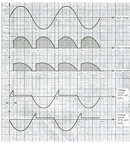
129 The heart of any voltage regulator is a control element. f such a element is connected in shunt with the load the regulator circuit is called shunt voltage regulator. BLOCK DAGRAM OF SHUNT OLTAGE REGULATOR 3. Explain how SCR can be used for power control[no/dec-06,,] 9

130 The SCR is an unidirectional device and like diode, it allows to flow current in only one direction. But unlike diode, it has a built in feature to switch ON and OFF. The switching of SCR is controlled by the additional input is called gate and biasing conidian. There are two types of controlling device DC power controlling using SCR AC power controlling using SCR DC power controlling using SCR 30

131 Single Phase Full Wave Rectifier n full wave rectifier both positive and negative half of ac supply is used and hence the average value of the dc voltage is high and ripple content is less compared to half wave rectifiers. There are two possible circuits arranging for obtaining full eave rectifiers. Using center tapped transformer Using bridge rectifier 3
132 3
133 33

![[APR/MAY-04] There are two types of regulators namely, Shunt voltage](/docs-images/74/71463996/images/134-1.jpg "regulator Series voltage regulator Each type provides a constant d.")
134 4. Describe in block diagram the series and shunt voltage regulator and explain it. [APR/MAY-04] There are two types of regulators namely, Shunt voltage regulator Series voltage regulator Each type provides a constant d.c output voltage which is regulated. SHUNT OLTAGE REGULATOR 34

135 SERES OLTAGE REGULATOR 35
136 5. Explain the operation of a half wave rectifier circuit with various parameters that govern its performance? [APR/MAY-0, ] The circuit of a half wave rectifier is shown in fig. below: Construction The rectifying element conducts only during positive half cycle of input ac supply. The negative half cycles of ac supply are eliminated from the output. This rectifier circuit consists of resistive load, rectifying element is p-n junction diode, and the source of ac voltage, all connected in series. Usually the rectifier circuits are operated from the ac mains supply. To obtain the desired dc voltage across the load, the ac voltage is applied to the rectifier circuit using suitable step up or step down transformer with suitable turns ratio. The input to the rectifier circuit shown above is a sinusoidal voltage. Let Rf be the forward resistance of the diode and when the diode is reverse biased, the diode almost acts as an open circuit, conducting no current. Operation During the positive half cycle of secondary ac voltage, terminal (A) becomes positive with respect to terminal (B). The diode is forward biased and the current flows in the circuit in the clockwise direction as shown in fig. below. The current will flow for almost full positive half cycle. This current is also flowing through load resistance R L, hence denoted as load current i L. 36

137 During negative half cycle, when terminal (A) is negative with respect to terminal (B), diode becomes reverse biased. Hence no current flows in the circuit as shown in figure above. Thus the circuit current is in the form of half sinusoidal pulses called pulsating dc. Similarly, the load voltage is also in the form of half sinusoidal pulses. Since the output is pulsating in nature, it is necessary to calculate the average value of load current and average value of output voltage. The load current can be mathematically expressed as i L = m sint, 0 < t < 0, <t < Performance parameters of half wave rectifier: Average DC load current: 37
138 The average or dc value of alternating current is obtained by integration. For finding out the average value of an alternating waveform, we have to determine the area under the curve over one complete cycle i.e from 0 to and then dividing it by the base i.e. Mathematically, current waveform can be described as, i L = m sin t for 0 t i L = 0 for t where m = peak value of load current DC = 0 ild( t) = 0 msin td( t) As current flows during negative half cycle of ac input voltage, i.e between t=,we change the limits of integration. DC = 0 msin td( t) DC = m = - [cos cos0] m = - [ ] m = average value Applying Kirchhoff s voltage law we can write, m = Esm Rf Rs RL Where R s = resistance of secondary winding of transformer. if R s is not given it should be neglected while calculating m. Average DC load voltage (E DC ) The average dc load voltage is the product of average dc load current and the load resistance R L. E DC = DC R L = mrl Esm = RL ( Rf Rs RL) The winding resistance R s and forward diode resistance R f are practically very small compared ro R L. 38
139 E DC = Esm Rf Rs [ ] RL But R f and R s are small compared to R L E DC = Esm RMS Load current ( rms ) The R.M.S means squaring, finding mean and then finding square root. Hence R.M.S value of load current can be obtained as, rms = [msin t]d ( t) 0 cost = m [ ] d( t) 0 = m t sin( ) { t } 4 0 = m ( ) m rms = D.C Power output (P DC ): The d.c power output can be obtained as, P DC =E DC DC = DC R L D.C power output = DCR L = [ m ] R L P DC =[ m ] R L Where m = Esm Rf RL Rs 39
140 P dc = EsmRL [ Rf RL Rs] A.C power input (P ac ) The power input taken from the secondary of transformer is the power supplied to three resistances namely R L, the diode resistance R f and winding resistance R s. The a.c power is given by, But rms = P ac = rms [R L + R f + R s ] m for half wave P ac = m /4 [R L +R f +R s ] Rectifier efficiency ( ) The rectifier efficiency is defined as the ratio of output d.c power to input a.c power. D. Coutputpower A. Cinputpower Pdc Pac (4 / ) RL ( Rf Rs RL) Rf Rs ( ) RL if (R f +R s ) << R L as mentioned earlier, we get the maximum theoretical efficiency of half wave rectifier as, % = X 00 = 40.6 % Thus in half wave rectifier, maximum 40.6% ac power gets converted to d.c power in the load. f the efficiency of rectifier is 40% then what happens to the remaining 60% power. t is present in terms of ripples in the output which is fluctuating component present in the output. Thus more the rectifier efficiency, less are ripple contents in the output. Ripple factor t is seen that the output of half wave rectifier is not pure dc but a pulsating dc. The output contains pulsating components called ripples. deally there should not be any ripples in the rectifier output. The measure of such ripples present in the output is with the help of a factor called ripple factor denoted by. t tells how smooth the output is. Smaller the ripple factor closer is the output to a pure dc. The ripple factor expresses how much successful the circuit is, in obtaining pure dc from ac input. 40
141 Mathematically ripple factor is defined as the ratio of R.M.S value of the ac component in the output to the average of dc component present in the output. Ripple factor = R. M. Svalueofaccomponent Averageordccomponent RMS alue of ac component = ac = RMS DC γ = RMS DC DC γ = RMS DC Substituting the values of RMS and DC, we get γ =. for half wave rectifier. Peak nverse oltage (P) The peak inverse voltage is the peak voltage across the diode in the reverse direction. For half wave rectifier the value of P is Esm. Transformer utilization factor (T.U.F) The factor which indicates how much is the utilization of the transformer in the circuit is called t transformer utilization factor. (T.U.F) DCpowertotheload T.U.F = ACpowerratingof secondary dcrl = Ermsrms = ( m / П) R L (Esm m / ) neglecting forward resistance R f of diode, E sm m R L oltage regulation T. U. F = m R L = 0.87 П m R L 4
142 The secondary voltage should not change with respect to the load current. The voltage regulation is the factor which tells us about the change in the dc output voltage as load changes from no load to full load condition. f ( dc ) NL = D.C voltage on no load ( dc ) FL = D.C voltage on full load Then voltage regulation is defined as, ( dc) NL ( dc) FL oltage regulation = ( dc) FL less the value of voltage regulation, better is the performance of rectifier circuit. For a full wave circuit, ( dc ) NL = Esm and П ( dc ) FL = dc R L the regulation can be expressed as, Rf Rs RL RL %R= 00 RL Rf Rs %R = 00 RL Neglecting winding resistance R s, the regulation can be expressed as, Rf %R = 00 RL Where R f = forward resistance of the diode. 6. Describe the working principle of full wave rectifier and derive its characteristic parameters? Full wave rectifier [APR/MAY-0,,][NO/ DEC-] The full wave rectifier conducts during both positive and negative half cycles of input a.c. supply. n order to rectify both the half cycles of a.c. input, two diodes are used in this circuit. The diodes feed a common load R L with the help of a center tap transformer. The a.c. voltage is applied through a suitable 4
143 power transformer with proper turns ratio. The full wave rectifier circuit is shown in fig For the proper operation of the circuit, a center-tap on the secondary winding of the transformer is essential. Operation of the circuit Consider the positive half cycle of ac input voltage in which terminal (A) is positive and terminal (B) negative. The diode D will be forward biased and hence will conduct; while diode D will be reverse biased and will act as an open circuit and will not conduct. The diode D supplies the load current, i.e i L = i d. This current is flowing through upper half of secondary winding while the lower half of secondary winding of the transformer carries no current since diode D is reverse biased and acts as an open circuit. n the next half cycle of ac voltage, polarity reverses and terminal (A) becomes negative and (B) positive. The diode D conducts, being forward biased, while D does not, being reverse biased. The diode D supplies the load current, i.e i L = i d. Now the lower half of the secondary winding carries the current but the upper half does not. Hence we get rectified output across the load. The load current is sum of individual diode currents flowing in corresponding half cycles. t is also noted that the two diodes do not conduct simultaneously but in alternate half cycles. The individual diode currents and the load current are shown in the fig Thus the full wave rectifier circuit essentially consist of two half-wave rectifier circuits working independently (working in alternate half cycles of ac) of each other but feeding a common load. The output load current is still pulsating d.c and not pure d.c. 43

144 Wave forms Maximum load current R f = forward resistance of diodes R s = winding resistance of each half of secondary R L = load resistance e s = instantaneous a.c. voltage across each half of secondary E sm = maximum value of a.c. input voltage across each half of secondary windinghence we can write the expression for the maximum value of the load current, looking at equivalent circuit shown in fig. 44
145 Average dc load current ( DC ) Consider one cycle of load current i L from 0 to to obtain the average value which is d.c value of load current. i L = m sin t 0 t But for to the current i L is again positive while sin t term is negative during to. Hence in the region to the positive i L can be represented as negative of m sin( t ) i L = - m sin t t av = DC = 0 ild( t) = [ msin td( t) msintd( t) ] 0 m = [ coscos0 coscos] But cos =- m = [ ( ) ( )] dc = m for full wave rectifier For half wave it is m / and full wave rectifier is the combination of two half wave circuits acting alternately in two half cycles of input. Hence obviously the d.c value for full wave circuit is m /. Average DC load voltage (E DC ) The d.c load voltage is, E DC = DC R L = Substituting value of m mrl 45
146 E DC = EsmRL Esm = [ Rf Rs RL] Rf Rs [ ] RL But as R f and R s << R L hence E DC = Esm Rf Rs RL << RMS Load current ( rms ) The RMS value of current can be obtained as follows: rms = 0 i Ld( t ) Since two half wave rectifier are similar in operation we can write, rms = [msin t]d ( t) 0 cost = m [ ] d( t) 0 rms = m t sin( ) { t } 0 = m [ 0] m rms = D.C Power output (P DC ) The d.c power output can be obtained as, P DC =E DC DC = dc R L D.C power output = m DCR L = [ ] R L P dc = 4 Esm X ( Rs Rf RL) R L 46
147 A.C power input (P ac ) The a.c power input is given by, P ac = rms [R L + R f + R s ] ( Rs Rf RL) P ac = m Substituting value of m we get, P ac = E smx (Rf +R s +R L ) ( Rs Rf RL) P ac = E sm ( Rf Rs RL) Rectifier efficiency ( ) The rectifier efficiency is defined as the ratio of output d.c power to input a.c power. D. Coutputpower A. Cinputpower Pdc Pac 8RL ( Rf Rs RL) Ripple factor ( ) but if R f +R s << R L,neglecting it from denominator 8RL ( RL) 8 8 % max 00 8.% This is the maximum theoretical efficiency of full wave rectifier. The ripple factor is given by a general expression, rms Ripple factor = [ ] dc 47
148 For full wave rms = m / and dc = m / Substituting in the above equation, m/ Ripple factor = [ ] m/ = 8 Ripple factor = = 0.48 This indicates that the ripple contents in the output are 48% of the d.c component which is much less than that for the half wave circuit. Peak inverse voltage (P) t can be observed from the circuit diagram that when diode is reversed biased then full transformer secondary voltage gets impressed across it. The drop across conducting diode is assumed zero. Thus the peak value of the inverse voltage to which diode gets subjected is voltage across both the parts of the transformer secondary. t can be seen that when D is reverse biased, point A is at E sm with respect to ground while point B is at + E sm with respect to ground, neglecting diode drop. Thus total peak voltage across D is E sm. P of diode = E sm = E dc dc =0 where E sm = maximum value of ac voltage across half the secondary of transformer. f the diode drop is considered to be 0.7 then the P of reverse biased diode is P of diode =E sm 0.7 This is because only one diode conducts at a time. Transformer utilization factor (T.U.F) n full wave rectifier, the secondary current flows through each half separately in every half cycle. While the primary of transformer carries current continuously. Hence T.U.F is calculated for primary and secondary windings separately and then the average T.U.F is determined. 48
149 DCpowertotheload Secondary T.U.F = ACpowerratingof secondary dcrl = Ermsrms RL Esm m =( m ) Neglecting Forward Resistance R f Of Diode, E sm m R l Secondary T.U.F =( 4 m 8 R L )/ ( m R L /) = =0.8 The primary of the transformer is feeding two half-wave rectifiers separately. These two half-wave rectifiers work independently of each other but feed a common load. We have already derived the T.U.F for half wave circuit to be equal to Hence T.U.F for primary winding= x T.U.F of half wave circuit. = x 0.87 =0.574 Average T.U.F for full Wave rectifier circuit = T. U. Fofprimary T. U. Fof secondary = = Thus in full-wave circuit transformer gets utilized more than the half wave rectifier. oltage regulation The secondary voltage should not change with respect to the load current. the voltage regulation is the factor which tells us about the change in the dc output voltage as load changes from no load to full load condition. f ( dc ) NL = D.C voltage on no load ( dc ) FL = D.C voltage on full load 49
150 then voltage regulation is defined as, ( dc) NL ( dc) FL voltage regulation = ( dc) FL less the value of voltage regulation, better is the performance of rectifier circuit. For a full wave circuit, ( dc ) NL = Esm and ( dc ) FL = dc R L the regulation can be expressed as, Now m = Esm %R =( ( dcrl)/ dc R L ) x 00 Esm Rf Rs RL E sm = m ( R f +R s +R L ) And dc = m Rf Rs RL RL %R= 00 RL Rf Rs %R = 00 RL Neglecting winding resistance R s, the regulation can be expressed as, Rf %R = 00 where R f = forward resistance of the diode. RL 6. Explain in detail the operation of full wave Bridge rectifier circuit [APR/MAY-0,] 50
151 7. Compare half wave, full wave and bridge rectifiers [DEC-007] 5

152 8. Explain in detail the operation of capacitive filter on and half and full wave rectifier operation. Principle we know Xc = /fc, if f is low, X C is high, i.e., capacitor does not permit dc or low frequency components pass through it. f f is high, then capacitor allows all ac high frequency component can pass through C instead of R L. Thus capacitor filter always resources all high frequency components. Half wave rectifier with capacitor filter Construction The half wave rectifier with a capacitor filter is shown in the fig. n this case the capacitor is connected in parallel with the output of the half wave rectifier, because, capacitor offers high reactance 5
153 Operation During the (first quarter of) positive half cycle of ac input, the diode D is forward biased hence it acts as switch and directly connects secondary across C. Now the capacitor quickly charges to a voltage m because there is no resistance in the charging path except diode forward resistance which, is negligible. When the input voltage falls (second quarter of positive half cycle) below the capacitor or m, i.e., i < c the diode becomes reverse biased ( D = in c) as result of this the capacitor started to discharge through the load resistor R L. During the negative half cycle, the diode D becomes reverse biased and it does not conduct, so the capacitor C continuously discharges through R L. As the discharging time constant ( = CR L ) is large, usually 00 times more than charging time, hence the capacitor does not have sufficient time to discharge appreciably. Due to this fact the voltage of capacitor C decreases slightly, this process is repeated till the next positive half cycle. 53
154 During the next positive half cycle, when the input voltage increases above the capacitor voltage (in > c), the diode becomes forward biased due to this the capacitor is charged towards its maximum value. The instant at which conduction stops is called the cut out point and the time at which the conduction starts is known as cut in point which is shown in fig. above. During cut-in to cut-off points, the diode current flows and diode voltage in these instants is greater than the capacitor voltage. Thus the diode current is a short duration of pulses i.e. a surging current. Hence the diode acts as a switch which permits charge to flow in capacitor when the input voltage exceeds the capacitor voltage and then disconnects the source when the input voltage falls below that of capacitor voltage. Circuit Diagram: Wave form: 54

155 Full wave rectifier with capacitive filter Construction t consists of either center tapped full wave rectifier or bridge type full wave rectifier with capacitor as filter which is connected across load resistor as shown in fig. We know the inductor filter is only suitable for the heavy loads. An inexpensive filter for light loads is found that the capacitor filter which is connected directly across the load. Operation ) During first half of positive half cycle the diode D is forward biased, D is reverse biased then the capacitor charges up to the peak value of the input voltage and tries to maintain this value in ) When the input voltage falls below m or c then (c < in) both diodes become reverse biased thus the capacitor starts discharging through the load resistor, it will continue until the input voltage exceeds the capacitor voltage. 3) During the negative half cycle of input, diode D is reverse biased and diode D is forward biased. When input voltage exceeds the capacitor voltage, the capacitor starts charging the same procedure is repeated for all cycle. 4) However, as the load increases, the discharge of capacitor C will be greater resulting in more ripple and lower dc output voltage. Wave from 55
Chapter Two "Bipolar Transistor Circuits"
 Chapter Two "Bipolar Transistor Circuits" 1.TRANSISTOR CONSTRUCTION:- The transistor is a three-layer semiconductor device consisting of either two n- and one p-type layers of material or two p- and one
DC Bias. Graphical Analysis. Script
 Course: B.Sc. Applied Physical Science (Computer Science) Year & Sem.: Ist Year, Sem - IInd Subject: Electronics Paper No.: V Paper Title: Analog Circuits Lecture No.: 3 Lecture Title: Analog Circuits
Transistor Biasing. DC Biasing of BJT. Transistor Biasing. Transistor Biasing 11/23/2018
 Transistor Biasing DC Biasing of BJT Satish Chandra Assistant Professor Department of Physics P P N College, Kanpur www.satish0402.weebly.com A transistors steady state of operation depends a great deal
Improving Amplifier Voltage Gain
 15.1 Multistage ac-coupled Amplifiers 1077 TABLE 15.3 Three-Stage Amplifier Summary HAND ANALYSIS SPICE RESULTS Voltage gain 998 1010 Input signal range 92.7 V Input resistance 1 M 1M Output resistance
BJT AC Analysis CHAPTER OBJECTIVES 5.1 INTRODUCTION 5.2 AMPLIFICATION IN THE AC DOMAIN
 BJT AC Analysis 5 CHAPTER OBJECTIVES Become familiar with the, hybrid, and hybrid p models for the BJT transistor. Learn to use the equivalent model to find the important ac parameters for an amplifier.
UNIT I BIASING OF DISCRETE BJT AND MOSFET PART A
 UNIT I BIASING OF DISCRETE BJT AND MOSFET PART A 1. Why do we choose Q point at the center of the load line? 2. Name the two techniques used in the stability of the q point.explain. 3. Give the expression
UNIT I - TRANSISTOR BIAS STABILITY
 UNIT I - TRANSISTOR BIAS STABILITY OBJECTIVE On the completion of this unit the student will understand NEED OF BIASING CONCEPTS OF LOAD LINE Q-POINT AND ITS STABILIZATION AND COMPENSATION DIFFERENT TYPES
Small signal ac equivalent circuit of BJT
 UNIT-2 Part A 1. What is an ac load line? [N/D 16] A dc load line gives the relationship between the q-point and the transistor characteristics. When capacitors are included in a CE transistor circuit,
EC2205 Electronic Circuits-1 UNIT III FREQUENCY RESPONSE OF AMPLIFIERS
 EC2205 Electronic Circuits-1 UNIT III FREQUENCY RESPONSE OF AMPLIFIERS PART A (2 MARK QUESTIONS) 1. Two amplifiers having gain 20 db and 40 db are cascaded. Find the overall gain in db. (NOV/DEC 2009)
BJT Circuits (MCQs of Moderate Complexity)
") BJT Circuits (MCQs of Moderate Complexity) 1. The current ib through base of a silicon npn transistor is 1+0.1 cos (1000πt) ma. At 300K, the rπ in the small signal model of the transistor is i b B C r
BJT Circuits (MCQs of Moderate Complexity) 1. The current ib through base of a silicon npn transistor is 1+0.1 cos (1000πt) ma. At 300K, the rπ in the small signal model of the transistor is i b B C r
Chapter Three " BJT Small-Signal Analysis "
 Chapter Three " BJT Small-Signal Analysis " We now begin to examine the small-signal ac response of the BJT amplifier by reviewing the models most frequently used to represent the transistor in the sinusoidal
Chapter 8. Field Effect Transistor
 Chapter 8. Field Effect Transistor Field Effect Transistor: The field effect transistor is a semiconductor device, which depends for its operation on the control of current by an electric field. There
Basic Electronics Prof. Dr. Chitralekha Mahanta Department of Electronics and Communication Engineering Indian Institute of Technology, Guwahati
 Basic Electronics Prof. Dr. Chitralekha Mahanta Department of Electronics and Communication Engineering Indian Institute of Technology, Guwahati Module: 3 Field Effect Transistors Lecture-8 Junction Field
fiziks Institute for NET/JRF, GATE, IIT-JAM, M.Sc. Entrance, JEST, TIFR and GRE in Physics
 nstitute for NT/JF, GAT, T-JAM, M.Sc. ntrance, JST, TF and G in Physics 3. ipolar Junction Transistors 3.1 Transistor onstruction Transistor is a three-layer semiconductor device consisting of either two
ESE319 Introduction to Microelectronics High Frequency BJT Model & Cascode BJT Amplifier
 High Frequency BJT Model & Cascode BJT Amplifier 1 Gain of 10 Amplifier Non-ideal Transistor C in R 1 V CC R 2 v s Gain starts dropping at > 1MHz. Why! Because of internal transistor capacitances that
Paper-1 (Circuit Analysis) UNIT-I
 UNIT-I") Paper-1 (Circuit Analysis) UNIT-I AC Fundamentals & Kirchhoff s Current and Voltage Laws 1. Explain how a sinusoidal signal can be generated and give the significance of each term in the equation? 2. Define
Paper-1 (Circuit Analysis) UNIT-I AC Fundamentals & Kirchhoff s Current and Voltage Laws 1. Explain how a sinusoidal signal can be generated and give the significance of each term in the equation? 2. Define
Gechstudentszone.wordpress.com
 UNIT 4: Small Signal Analysis of Amplifiers 4.1 Basic FET Amplifiers In the last chapter, we described the operation of the FET, in particular the MOSFET, and analyzed and designed the dc response of circuits
BASIC ELECTRONICS PROF. T.S. NATARAJAN DEPT OF PHYSICS IIT MADRAS
 BASIC ELECTRONICS PROF. T.S. NATARAJAN DEPT OF PHYSICS IIT MADRAS LECTURE-13 Basic Characteristic of an Amplifier Simple Transistor Model, Common Emitter Amplifier Hello everybody! Today in our series
ANALOG FUNDAMENTALS C. Topic 4 BASIC FET AMPLIFIER CONFIGURATIONS
 AV18-AFC ANALOG FUNDAMENTALS C Topic 4 BASIC FET AMPLIFIER CONFIGURATIONS 1 ANALOG FUNDAMENTALS C AV18-AFC Overview This topic identifies the basic FET amplifier configurations and their principles of
Document Name: Electronic Circuits Lab. Facebook: Twitter:
 Document Name: Electronic Circuits Lab www.vidyathiplus.in Facebook: www.facebook.com/vidyarthiplus Twitter: www.twitter.com/vidyarthiplus Copyright 2011-2015 Vidyarthiplus.in (VP Group) Page 1 CIRCUIT
FREQUENTLY ASKED QUESTIONS
 FREQUENTLY ASKED QUESTIONS UNIT-1 SUBJECT : ELECTRONIC DEVICES AND CIRCUITS SUBJECT CODE : EC6202 BRANCH: EEE PART -A 1. What is meant by diffusion current in a semi conductor? (APR/MAY 2010, 2011, NOV/DEC
R a) Draw and explain VI characteristics of Si & Ge diode. (8M) b) Explain the operation of SCR & its characteristics (8M)
 Draw and explain VI characteristics of Si & Ge diode. (8M) b) Explain the operation of SCR & its characteristics (8M)") SET - 1 1. a) Define i) transient capacitance ii) Diffusion capacitance (4M) b) Explain Fermi level in intrinsic and extrinsic semiconductor (4M) c) Derive the expression for ripple factor of Half wave
SET - 1 1. a) Define i) transient capacitance ii) Diffusion capacitance (4M) b) Explain Fermi level in intrinsic and extrinsic semiconductor (4M) c) Derive the expression for ripple factor of Half wave
Analog Electronics. Electronic Devices, 9th edition Thomas L. Floyd Pearson Education. Upper Saddle River, NJ, All rights reserved.
 Analog Electronics BJT Structure The BJT has three regions called the emitter, base, and collector. Between the regions are junctions as indicated. The base is a thin lightly doped region compared to the
SIDDHARTH GROUP OF INSTITUTIONS :: PUTTUR (AUTONOMOUS) Siddharth Nagar, Narayanavanam Road QUESTION BANK
 Siddharth Nagar, Narayanavanam Road QUESTION BANK") SIDDHARTH GROUP OF INSTITUTIONS :: PUTTUR (AUTONOMOUS) Siddharth Nagar, Narayanavanam Road 517583 QUESTION BANK Subject with Code : Electronic Circuit Analysis (16EC407) Year & Sem: II-B.Tech & II-Sem
SIDDHARTH GROUP OF INSTITUTIONS :: PUTTUR (AUTONOMOUS) Siddharth Nagar, Narayanavanam Road 517583 QUESTION BANK Subject with Code : Electronic Circuit Analysis (16EC407) Year & Sem: II-B.Tech & II-Sem
Transistor Biasing and Operational amplifier fundamentals. OP-amp Fundamentals and its DC characteristics. BJT biasing schemes
 Lab 1 Transistor Biasing and Operational amplifier fundamentals Experiment 1.1 Experiment 1.2 BJT biasing OP-amp Fundamentals and its DC characteristics BJT biasing schemes 1.1 Objective 1. To sketch potential
Field Effect Transistors
 Field Effect Transistors Purpose In this experiment we introduce field effect transistors (FETs). We will measure the output characteristics of a FET, and then construct a common-source amplifier stage,
UNIT 3: FIELD EFFECT TRANSISTORS
 FIELD EFFECT TRANSISTOR: UNIT 3: FIELD EFFECT TRANSISTORS The field effect transistor is a semiconductor device, which depends for its operation on the control of current by an electric field. There are
Homework Assignment 12
 Homework Assignment 12 Question 1 Shown the is Bode plot of the magnitude of the gain transfer function of a constant GBP amplifier. By how much will the amplifier delay a sine wave with the following
Scheme Q.1 Attempt any SIX of following: 12-Total Marks a) Draw symbol NPN and PNP transistor. 2 M Ans: Symbol Of NPN and PNP BJT (1M each)
 Draw symbol NPN and PNP transistor. 2 M Ans: Symbol Of NPN and PNP BJT (1M each)") Q. No. WINTER 16 EXAMINATION (Subject Code: 17319) Model Answer Important Instructions to examiners: 1) The answers should be examined by key words and not as word-to-word as given in the model answer
Q. No. WINTER 16 EXAMINATION (Subject Code: 17319) Model Answer Important Instructions to examiners: 1) The answers should be examined by key words and not as word-to-word as given in the model answer
Electronics Lab. (EE21338)
") Princess Sumaya University for Technology The King Abdullah II School for Engineering Electrical Engineering Department Electronics Lab. (EE21338) Prepared By: Eng. Eyad Al-Kouz October, 2012 Table of
Princess Sumaya University for Technology The King Abdullah II School for Engineering Electrical Engineering Department Electronics Lab. (EE21338) Prepared By: Eng. Eyad Al-Kouz October, 2012 Table of
BJT. Bipolar Junction Transistor BJT BJT 11/6/2018. Dr. Satish Chandra, Assistant Professor, P P N College, Kanpur 1
 BJT Bipolar Junction Transistor Satish Chandra Assistant Professor Department of Physics P P N College, Kanpur www.satish0402.weebly.com The Bipolar Junction Transistor is a semiconductor device which
Electronics Prof. D. C. Dube Department of Physics Indian Institute of Technology, Delhi
 Electronics Prof. D. C. Dube Department of Physics Indian Institute of Technology, Delhi Module No # 05 FETS and MOSFETS Lecture No # 06 FET/MOSFET Amplifiers and their Analysis In the previous lecture
Unit- I- Biasing Of Discrete BJT and MOSFET
 Part- A QUESTIONS: Unit- I- Biasing Of Discrete BJT and MOSFET 1. Describe about BJT? BJT consists of 2 PN junctions. It has three terminals: emitter, base and collector. Transistor can be operated in
 Code No: Y0221/R07 Set No. 1 I B.Tech Supplementary Examinations, Apr/May 2013 BASIC ELECTRONIC DEVICES AND CIRCUITS (Electrical & Electronics Engineering) Time: 3 hours Max Marks: 80 Answer any FIVE Questions
UNIT 4 BIASING AND STABILIZATION
 UNIT 4 BIASING AND STABILIZATION TRANSISTOR BIASING: To operate the transistor in the desired region, we have to apply external dec voltages of correct polarity and magnitude to the two junctions of the
Video Course on Electronics Prof. D. C. Dube Department of Physics Indian Institute of Technology, Delhi
 Video Course on Electronics Prof. D. C. Dube Department of Physics Indian Institute of Technology, Delhi Module No. # 02 Transistors Lecture No. # 09 Biasing a Transistor (Contd) We continue our discussion
DEPARTMENT OF ELECTRONICS AND COMMUNICATION ENGINEERING III SEMESTER EC 6304 ELECTRONIC CIRCUITS I. (Regulations 2013)
") DEPARTMENT OF ELECTRONICS AND COMMUNICATION ENGINEERING III SEMESTER EC 6304 ELECTRONIC CIRCUITS I (Regulations 2013 UNIT-1 Part A 1. What is a Q-point? [N/D 16] The operating point also known as quiescent
DEPARTMENT OF ELECTRONICS AND COMMUNICATION ENGINEERING III SEMESTER EC 6304 ELECTRONIC CIRCUITS I (Regulations 2013 UNIT-1 Part A 1. What is a Q-point? [N/D 16] The operating point also known as quiescent
4.2.2 Metal Oxide Semiconductor Field Effect Transistor (MOSFET)
") 4.2.2 Metal Oxide Semiconductor Field Effect Transistor (MOSFET) The Metal Oxide Semitonductor Field Effect Transistor (MOSFET) has two modes of operation, the depletion mode, and the enhancement mode.
4.2.2 Metal Oxide Semiconductor Field Effect Transistor (MOSFET) The Metal Oxide Semitonductor Field Effect Transistor (MOSFET) has two modes of operation, the depletion mode, and the enhancement mode.
Basic Electronics Prof. Dr. Chitralekha Mahanta Department of Electronics and Communication Engineering Indian Institute of Technology, Guwahati
 Basic Electronics Prof. Dr. Chitralekha Mahanta Department of Electronics and Communication Engineering Indian Institute of Technology, Guwahati Module: 2 Bipolar Junction Transistors Lecture-1 Transistor
(Refer Slide Time: 01:33)
") Solid State Devices Dr. S. Karmalkar Department of Electronics and Communication Engineering Indian Institute of Technology, Madras Lecture - 31 Bipolar Junction Transistor (Contd ) So, we have been discussing
Solid State Devices Dr. S. Karmalkar Department of Electronics and Communication Engineering Indian Institute of Technology, Madras Lecture - 31 Bipolar Junction Transistor (Contd ) So, we have been discussing
By: Dr. Ahmed ElShafee
 Lecture (04) Transistor Bias Circuit 3 BJT Amplifiers 1 By: Dr. Ahmed ElShafee ١ Emitter Feedback Bias If an emitter resistor is added to the base bias circuit in Figure, the result is emitter feedback
KOM2751 Analog Electronics :: Dr. Muharrem Mercimek :: YTU - Control and Automation Dept. 1 2 (CONT D - II) DIODE APPLICATIONS
 DIODE APPLICATIONS") KOM2751 Analog Electronics :: Dr. Muharrem Mercimek :: YTU - Control and Automation Dept. 1 2 (CONT D - II) DIODE APPLICATIONS Most of the content is from the textbook: Electronic devices and circuit theory,
KOM2751 Analog Electronics :: Dr. Muharrem Mercimek :: YTU - Control and Automation Dept. 1 2 (CONT D - II) DIODE APPLICATIONS Most of the content is from the textbook: Electronic devices and circuit theory,
Subject Code: Model Answer Page No: / N
 Important Instructions to examiners: 1) The answers should be examined by key words and not as word-to-word as given in the model answer scheme. 2) The model answer and the answer written by candidate
(a) BJT-OPERATING MODES & CONFIGURATIONS
 BJT-OPERATING MODES & CONFIGURATIONS") (a) BJT-OPERATING MODES & CONFIGURATIONS 1. The leakage current I CBO flows in (a) The emitter, base and collector leads (b) The emitter and base leads. (c) The emitter and collector leads. (d) The base
(a) BJT-OPERATING MODES & CONFIGURATIONS 1. The leakage current I CBO flows in (a) The emitter, base and collector leads (b) The emitter and base leads. (c) The emitter and collector leads. (d) The base
SMALL SINGLE LOW FREQUENCY TRANSISTOR AMPLIFIERS
 UNIT VI SMALL SINGLE LOW FREQUENCY TRANSISTOR 6.1 Introduction AMPLIFIERS V-I characteristics of an active device such as BJT are non-linear. The analysis of a non- linear device is complex. Thus to simplify
INSTITUTE OF AERONAUTICAL ENGINEERING (AUTONOMUS) Dundigal, Hyderabad
 Dundigal, Hyderabad") INSTITUTE OF AERONAUTICAL ENGINEERING (AUTONOMUS) Dundigal, Hyderabad - 00 0 ELECTRONICS AND COMMUNICATION ENGINEERING ASSIGNMENT Name : ELECTRONIC CIRCUIT ANALYSIS Code : A0 Class : II - B. Tech nd semester
INSTITUTE OF AERONAUTICAL ENGINEERING (AUTONOMUS) Dundigal, Hyderabad - 00 0 ELECTRONICS AND COMMUNICATION ENGINEERING ASSIGNMENT Name : ELECTRONIC CIRCUIT ANALYSIS Code : A0 Class : II - B. Tech nd semester
Chapter 3: Bipolar Junction Transistors
 Chapter 3: Bipolar Junction Transistors Transistor Construction There are two types of transistors: pnp npn pnp The terminals are labeled: E - Emitter B - Base C - Collector npn 2 Transistor Operation
Emitter base bias. Collector base bias Active Forward Reverse Saturation forward Forward Cut off Reverse Reverse Inverse Reverse Forward
 SEMICONDUCTOR PHYSICS-2 [Transistor, constructional characteristics, biasing of transistors, transistor configuration, transistor as an amplifier, transistor as a switch, transistor as an oscillator] Transistor
5.25Chapter V Problem Set
 5.25Chapter V Problem Set P5.1 Analyze the circuits in Fig. P5.1 and determine the base, collector, and emitter currents of the BJTs as well as the voltages at the base, collector, and emitter terminals.
MODULE-2: Field Effect Transistors (FET)
") FORMAT-1B Definition: MODULE-2: Field Effect Transistors (FET) FET is a three terminal electronic device used for variety of applications that match with BJT. In FET, an electric field is established by
FORMAT-1B Definition: MODULE-2: Field Effect Transistors (FET) FET is a three terminal electronic device used for variety of applications that match with BJT. In FET, an electric field is established by
EC1203: ELECTRONICS CIRCUITS-I UNIT-I TRANSISTOR BIASING PART-A
 SHRI ANGALAMMAN COLLEGE OF ENGG & TECH., TRICHY 621105 (Approved by AICTE, New Delhi and Affiliated to Anna University Chennai/Trichy) ( ISO 9001:2008 Certified Institution) DEPARTMENT OF ELECTRONICS &
(Refer Slide Time: 05:47)
") Solid State Devices Dr. S. Karmalkar Department of Electronics and Communication Engineering Indian Institute of Technology, Madras Lecture - 29 Bipolar Junction Transistor (Contd ) So we have been discussing
Solid State Devices Dr. S. Karmalkar Department of Electronics and Communication Engineering Indian Institute of Technology, Madras Lecture - 29 Bipolar Junction Transistor (Contd ) So we have been discussing
Bipolar Junction Transistors
 Bipolar Junction Transistors Invented in 1948 at Bell Telephone laboratories Bipolar junction transistor (BJT) - one of the major three terminal devices Three terminal devices more useful than two terminal
Expanded Answer: Transistor Amplifier Problem in January/February 2008 Morseman Column
 Expanded Answer: Transistor Amplifier Problem in January/February 2008 Morseman Column Here s what I asked: This month s problem: Figure 4(a) shows a simple npn transistor amplifier. The transistor has
ET215 Devices I Unit 4A
 ITT Technical Institute ET215 Devices I Unit 4A Chapter 3, Section 3.1-3.2 This unit is divided into two parts; Unit 4A and Unit 4B Chapter 3 Section 3.1 Structure of Bipolar Junction Transistors The basic
Bipolar Junction Transistors (BJTs) Overview
 Overview") 1 Bipolar Junction Transistors (BJTs) Asst. Prof. MONTREE SIRIPRUCHYANUN, D. Eng. Dept. of Teacher Training in Electrical Engineering, Faculty of Technical Education King Mongkut s Institute of Technology
1 Bipolar Junction Transistors (BJTs) Asst. Prof. MONTREE SIRIPRUCHYANUN, D. Eng. Dept. of Teacher Training in Electrical Engineering, Faculty of Technical Education King Mongkut s Institute of Technology
Integrated Circuit: Classification:
 Integrated Circuit: It is a miniature, low cost electronic circuit consisting of active and passive components that are irreparably joined together on a single crystal chip of silicon. Classification:
Diode and Bipolar Transistor Circuits
 Diode and Bipolar Transistor Circuits 2 2.1 A Brief Review of Semiconductors Semiconductors are crystalline structures in which each atom shares its valance electrons with the neighboring atoms. The simple
UNIT II MIDBAND ANALYSIS OF SMALL SIGNAL AMPLIFIERS
 UNIT II MIDBAND ANALYSIS OF SMALL SIGNAL AMPLIFIERS CE, CB and CC amplifiers. Method of drawing small-signal equivalent circuit. Midband analysis of various types of single stage amplifiers to obtain gain,
Phy 335, Unit 4 Transistors and transistor circuits (part one)
") Mini-lecture topics (multiple lectures): Phy 335, Unit 4 Transistors and transistor circuits (part one) p-n junctions re-visited How does a bipolar transistor works; analogy with a valve Basic circuit
Mini-lecture topics (multiple lectures): Phy 335, Unit 4 Transistors and transistor circuits (part one) p-n junctions re-visited How does a bipolar transistor works; analogy with a valve Basic circuit
CHAPTER 1 DIODE CIRCUITS. Semiconductor act differently to DC and AC currents
 CHAPTER 1 DIODE CIRCUITS Resistance levels Semiconductor act differently to DC and AC currents There are three types of resistances 1. DC or static resistance The application of DC voltage to a circuit
Physics 623 Transistor Characteristics and Single Transistor Amplifier Sept. 12, 2017
 Physics 623 Transistor Characteristics and Single Transistor Amplifier Sept. 12, 2017 1 Purpose To measure and understand the common emitter transistor characteristic curves. To use the base current gain
Course Number Section. Electronics I ELEC 311 BB Examination Date Time # of pages. Final August 12, 2005 Three hours 3 Instructor
 Course Number Section Electronics ELEC 311 BB Examination Date Time # of pages Final August 12, 2005 Three hours 3 nstructor Dr. R. Raut M aterials allowed: No Yes X (Please specify) Calculators allowed:
Bipolar Junction Transistor (BJT) Basics- GATE Problems
 Basics- GATE Problems") Bipolar Junction Transistor (BJT) Basics- GATE Problems One Mark Questions 1. The break down voltage of a transistor with its base open is BV CEO and that with emitter open is BV CBO, then (a) BV CEO =
Bipolar Junction Transistor (BJT) Basics- GATE Problems One Mark Questions 1. The break down voltage of a transistor with its base open is BV CEO and that with emitter open is BV CBO, then (a) BV CEO =
Code: 9A Answer any FIVE questions All questions carry equal marks *****
 II B. Tech II Semester (R09) Regular & Supplementary Examinations, April/May 2012 ELECTRONIC CIRCUIT ANALYSIS (Common to EIE, E. Con. E & ECE) Time: 3 hours Max Marks: 70 Answer any FIVE questions All
SAMPLE FINAL EXAMINATION FALL TERM
 ENGINEERING SCIENCES 154 ELECTRONIC DEVICES AND CIRCUITS SAMPLE FINAL EXAMINATION FALL TERM 2001-2002 NAME Some Possible Solutions a. Please answer all of the questions in the spaces provided. If you need
The Common Emitter Amplifier Circuit
 The Common Emitter Amplifier Circuit In the Bipolar Transistor tutorial, we saw that the most common circuit configuration for an NPN transistor is that of the Common Emitter Amplifier circuit and that
The Common Source JFET Amplifier
 The Common Source JFET Amplifier Small signal amplifiers can also be made using Field Effect Transistors or FET's for short. These devices have the advantage over bipolar transistors of having an extremely
AE103 ELECTRONIC DEVICES & CIRCUITS DEC 2014
 Q.2 a. State and explain the Reciprocity Theorem and Thevenins Theorem. a. Reciprocity Theorem: If we consider two loops A and B of network N and if an ideal voltage source E in loop A produces current
ES 330 Electronics II Homework # 1 (Fall 2016 SOLUTIONS)
") SOLUTIONS ES 330 Electronics II Homework # 1 (Fall 2016 SOLUTIONS) Problem 1 (20 points) We know that a pn junction diode has an exponential I-V behavior when forward biased. The diode equation relating
SOLUTIONS ES 330 Electronics II Homework # 1 (Fall 2016 SOLUTIONS) Problem 1 (20 points) We know that a pn junction diode has an exponential I-V behavior when forward biased. The diode equation relating
BJT Amplifier. Superposition principle (linear amplifier)
") BJT Amplifier Two types analysis DC analysis Applied DC voltage source AC analysis Time varying signal source Superposition principle (linear amplifier) The response of a linear amplifier circuit excited
BJT Amplifier Two types analysis DC analysis Applied DC voltage source AC analysis Time varying signal source Superposition principle (linear amplifier) The response of a linear amplifier circuit excited
II/IV B. TECH. DEGREE EXAMINATIONS, NOVEMBER Second Semester EC/EE ELECTRONIC CIRCUIT ANALYSIS. Time : Three Hours Max.
 Total No. of Questions : 9] [Total No. of Pages : 02 B.Tech. II/ IV YEAR DEGREE EXAMINATION, APRIL/MAY - 2014 (Second Semester) EC/EE/EI Electronic Circuit Analysis Time : 03 Hours Maximum Marks : 70 Q1)
MAHARASHTRA STATE BOARD OF TECHNICAL EDUCATION (Autonomous) (ISO/IEC Certified) MODEL ANSWER
 (ISO/IEC Certified) MODEL ANSWER") Important Instructions to examiners: 1) The answers should be examined by key words and not as word-to-word as given in the model answer scheme. 2) The model answer and the answer written by candidate
Important Instructions to examiners: 1) The answers should be examined by key words and not as word-to-word as given in the model answer scheme. 2) The model answer and the answer written by candidate
Section 2.3 Bipolar junction transistors - BJTs
 Section 2.3 Bipolar junction transistors - BJTs Single junction devices, such as p-n and Schottkty diodes can be used to obtain rectifying I-V characteristics, and to form electronic switching circuits
Module-1 BJT AC Analysis: The re Transistor Model. Common-Base Configuration
 Module-1 BJT AC Analysis: BJT AC Analysis: BJT AC Analysis: BJT Transistor Modeling, The re transistor model, Common emitter fixed bias, Voltage divider bias, Emitter follower configuration. Darlington
Physics 116A Fall 2000: Final Exam
 Physics 6A Fall 2000: Final Exam 2//2000 (rev. 2/0) Closed book and notes except for three 8.5 in 2 sheets of paper. Show reasoning for full credit. There are 6 problems and 200 points. Note: complex quantities
BASIC ELECTRONICS PROF. T.S. NATARAJAN DEPT OF PHYSICS IIT MADRAS
 BASIC ELECTRONICS PROF. T.S. NATARAJAN DEPT OF PHYSICS IIT MADRAS LECTURE-12 TRANSISTOR BIASING Emitter Current Bias Thermal Stability (RC Coupled Amplifier) Hello everybody! In our series of lectures
CENTURION UNIVERSITY OF TECHNOLOGY AND MANAGEMENT SCHOOL OF ENGINEERING & TECHNOLOGYDEPARTMENT OF ELECTRONICS & COMMUNICATION ENGINEERING
 CENTURION UNIVERSITY OF TECHNOLOGY AND MANAGEMENT SCHOOL OF ENGINEERING & TECHNOLOGYDEPARTMENT OF ELECTRONICS & COMMUNICATION ENGINEERING ELECTRONIC DEVICES Section: ECE SEM: II PART-A 1. a) In a N-type
FIELD EFFECT TRANSISTOR (FET) 1. JUNCTION FIELD EFFECT TRANSISTOR (JFET)
 1. JUNCTION FIELD EFFECT TRANSISTOR (JFET)") FIELD EFFECT TRANSISTOR (FET) The field-effect transistor (FET) is a three-terminal device used for a variety of applications that match, to a large extent, those of the BJT transistor. Although there
FIELD EFFECT TRANSISTOR (FET) The field-effect transistor (FET) is a three-terminal device used for a variety of applications that match, to a large extent, those of the BJT transistor. Although there
UNIT-1 Bipolar Junction Transistors. Text Book:, Microelectronic Circuits 6 ed., by Sedra and Smith, Oxford Press
 UNIT-1 Bipolar Junction Transistors Text Book:, Microelectronic Circuits 6 ed., by Sedra and Smith, Oxford Press Figure 6.1 A simplified structure of the npn transistor. Microelectronic Circuits, Sixth
ANALYSIS OF AN NPN COMMON-EMITTER AMPLIFIER
 ANALYSIS OF AN NPN COMMON-EMITTER AMPLIFIER Experiment Performed by: Michael Gonzalez Filip Rege Alexis Rodriguez-Carlson Report Written by: Filip Rege Alexis Rodriguez-Carlson November 28, 2007 Objectives:
Chapter 15 Goals. ac-coupled Amplifiers Example of a Three-Stage Amplifier
 Chapter 15 Goals ac-coupled multistage amplifiers including voltage gain, input and output resistances, and small-signal limitations. dc-coupled multistage amplifiers. Darlington configuration and cascode
PHYS 3152 Methods of Experimental Physics I E2. Diodes and Transistors 1
 Part I Diodes Purpose PHYS 3152 Methods of Experimental Physics I E2. In this experiment, you will investigate the current-voltage characteristic of a semiconductor diode and examine the applications of
TUNED AMPLIFIERS 5.1 Introduction: Coil Losses:
 TUNED AMPLIFIERS 5.1 Introduction: To amplify the selective range of frequencies, the resistive load R C is replaced by a tuned circuit. The tuned circuit is capable of amplifying a signal over a narrow
Common-Emitter Amplifier
 Dr. Charles Kim Common-Emitter Amplifier A. Before We Start As the title of this lab says, this lab is about designing a Common-Emitter Amplifier, and this in this stage of the lab course is premature,
The shape of the waveform will be the same, but its level is shifted either upward or downward. The values of the resistor R and capacitor C affect
 Diode as Clamper A clamping circuit is used to place either the positive or negative peak of a signal at a desired level. The dc component is simply added or subtracted to/from the input signal. The clamper
ECE321 Electronics I Fall 2006
 ECE321 Electronics I Fall 2006 Professor James E. Morris Lecture 11 31 st October, 2006 Bipolar Junction Transistors (BJTs) 5.1 Device Structure & Physics 5.2 I-V Characteristics Convert 5.1 information
CHAPTER 3: BIPOLAR JUNCION TRANSISTOR DR. PHẠM NGUYỄN THANH LOAN
 CHAPTER 3: BIPOLAR JUNCION TRANSISTOR DR. PHẠM NGUYỄN THANH LOAN Hanoi, 9/24/2012 Contents 2 Structure and operation of BJT Different configurations of BJT Characteristic curves DC biasing method and analysis
 UNIVERSITY PART-A ANSWERS Unit-1 1. What is an amplifier? An amplifier is a device which produces a large electrical output of similar characteristics to that of the input parameters. 2. What are transistors?
Chapter 8: Field Effect Transistors
 Chapter 8: Field Effect Transistors Transistors are different from the basic electronic elements in that they have three terminals. Consequently, we need more parameters to describe their behavior than
MODEL ANSWER SUMMER 17 EXAMINATION 17319
 MODEL ANSWER SUMMER 17 EXAMINATION 17319 Subject Title: Electronics Devices and Circuits. Subject Code: Important Instructions to examiners: 1) The answers should be examined by key words and not as word-to-word
Electronic Circuits II - Revision
 Electronic Circuits II - Revision -1 / 16 - T & F # 1 A bypass capacitor in a CE amplifier decreases the voltage gain. 2 If RC in a CE amplifier is increased, the voltage gain is reduced. 3 4 5 The load
Linear electronic. Lecture No. 1
 1 Lecture No. 1 2 3 4 5 Lecture No. 2 6 7 8 9 10 11 Lecture No. 3 12 13 14 Lecture No. 4 Example: find Frequency response analysis for the circuit shown in figure below. Where R S =4kR B1 =8kR B2 =4k R
Chapter 5 Transistor Bias Circuits
 Chapter 5 Transistor Bias Circuits Objectives Discuss the concept of dc biasing of a transistor for linear operation Analyze voltage-divider bias, base bias, and collector-feedback bias circuits. Basic
Lecture 3: Transistors
 Lecture 3: Transistors Now that we know about diodes, let s put two of them together, as follows: collector base emitter n p n moderately doped lightly doped, and very thin heavily doped At first glance,
Unit WorkBook 4 Level 4 ENG U19 Electrical and Electronic Principles LO4 Digital & Analogue Electronics 2018 Unicourse Ltd. All Rights Reserved.
 Pearson BTEC Levels 4 Higher Nationals in Engineering (RQF) Unit 19: Electrical and Electronic Principles Unit Workbook 4 in a series of 4 for this unit Learning Outcome 4 Digital & Analogue Electronics
Tutorial 2 BJTs, Transistor Bias Circuits, BJT Amplifiers FETs and FETs Amplifiers. Part 1: BJTs, Transistor Bias Circuits and BJT Amplifiers
 Tutorial 2 BJTs, Transistor Bias Circuits, BJT Amplifiers FETs and FETs Amplifiers Part 1: BJTs, Transistor Bias Circuits and BJT Amplifiers 1. Explain the purpose of a thin, lightly doped base region.
Bipolar junction transistors.
 Bipolar junction transistors. Third Semester Course code : 15EECC202 Analog electronic circuits (AEC) Team: Dr. Nalini C Iyer, R.V. Hangal, Sujata N, Prashant A, Sneha Meti AEC Team, Faculty, School of
Basic Electronics Prof. Dr. Chitralekha Mahanta Department of Electronics and Communication Engineering Indian Institute of Technology, Guwahati
 Basic Electronics Prof. Dr. Chitralekha Mahanta Department of Electronics and Communication Engineering Indian Institute of Technology, Guwahati Module: 3 Field Effect Transistors Lecture-7 High Frequency
Chapter 3 Bipolar Junction Transistors (BJT)
") Chapter 3 Bipolar Junction Transistors (BJT) Transistors In analog circuits, transistors are used in amplifiers and linear regulated power supplies. In digital circuits they function as electrical switches,
Chapter 3 Bipolar Junction Transistors (BJT) Transistors In analog circuits, transistors are used in amplifiers and linear regulated power supplies. In digital circuits they function as electrical switches,