Thinning of IC chips
|
|
|
- Spencer Welch
- 6 years ago
- Views:
Transcription
1 1 Thinning of IC chips Annette Teng CORWIL TECHNOLOGY CORP McCarthy Blvd. Milpitas, CA CONTENT Industry Demand for thinness Method to achieve ultrathin dies Mechanical testing of ultrathin die Die strength variation source Methods to achieve strong ultrathin dies Assembly of Ultrathin dies Die Attach Films Interconnection

2 3 Reasons to go thin Decrease street width Stackable 3D packaging Smart cards Improved Heat dissipation Better electrical performance Higher speeds Ultra Paper thin Embedded packaging Wearable packaging -Appliques Skin patch Implantable Foldable 3D die -cylinders -cones -origami inemi Roadmap International Electronic Manufacturing Initiative 4

3 5 6


4 7 STATSchipPAC ECTC um flip chip Conventional Flow for Wafer Thinning (DAG) 8 Patterned Full thickness Wafer Apply front side tape Backgrind Wafer Wash wafer BACKGRIND Die Pick and place Singulate/dicing Laser or Blade Remove front side tape Mount dicing tape on backside of wafer SAW

5 9 DAG Results: LOW YIELD Warpage & curl Non conformal Transport challenge Storage challenge Lamination challenge Dice Before Grind DBG Flow Comparison 10 Conventional method DBG DAG


6 Dice Before Grind Method 11 Singulation Depth Rough grind 300 grit Removed thickness Trench depth Fine grind>2000 Final thickness Front side tape 12 Results No Wafer Warpage & curl No Wafer Breakage Conformal Transportable Storable Easy to Laminate Easier to bond/debond


7 32um after DBG with Polygrind wheel 13 Sidewall Flaws Punctures 14 15um silicon die attached to package by 25um DAF. 20um gold wire bond


 M.Y.Tsai, ASE et al Radius 0.1;0.")
8 Thin die Strength Characterization Techniques 15 width T=0.150 F radius L 2 Point Test width 3F*length Strength = *width*thickness 2 F r=0.025 L= 0.570mm T= Point Test width 3F*length Strength = width*thickness 2 l F r=0.025 T= Point Test Fracture strength Test Methods 16 Point Load test (PLT) Radius 0.1; 0.25; 0.3mm Plate on Elastic Foundation Test (PEFT) M.Y.Tsai, ASE et al Radius 0.1;0.25;0.3mm 1.4mm silicone Ball & Ring Test Radii (ball, ring) Radius 0.1;0.25;0.3mm 1.4mm silicone diameter
9 7 Thickness SCV Chapter, CPMT Society, IEEE January 28, Relative Strength Breaking-Strength F*length Strength = *width*thickness (µm), Ball-Ring-Method, only ground, backside untreated Die thickness(mils) Effect of flaw size on Die strength Silicon Dice after grind (DAG).125mmThick M P a s c a l T 0.1T 0.2T 0.3T Ratio of sidewall crack to die thickness
10 Effect of flaw size on strength Silicon DBG 0.150mm thick 1200 M 1000 P a 800 s c 600 a l T 0.1T 0.2T 0.3T 0.4T Dramatic strength variation 20 D i e s t r e n g t h ( M p a ) A B C D E F G H
11 21 Die Strength of various 0.150mm thick.670mm RFID dies Fracture 400 strength in N/mm Finish and dicing method 22 Distribution plot -sample size 50 Group H (CMP-blade saw) F r e q u e n c y Die strength in MPa
12 23 F r e q u e n c y Distribution plot -sample size 50 Group H (CMP-blade saw) Die strength in MPa 24 Distribution plot of 2000grit etched group 16 F r e q u e n c y to to to to to to to 409 Die strength of singulated random dies from 1 wafer
13 25 Examples of Surface defects Most common chipout is last side rip of the Smaller piece Snaps off Shifts away from blade Vibrates more.150mm Smaller Y channel Blade feed direction X channel blade step direction blade Bigger Large fracture strength variations within 1 wafer MPa Angle from Anvil


14 Laser generated roughness 27 Laser ablation SIDEWALL 0.250mm SIDEWALL 0.250mm 28 Laser scribe and break SIDEWALL 0.250mm Laser Stealth and expand


15 29 PERSONAL PREFERENCE - VISUAL REJECT ACCEPT Examples of Surface Flaws 30
 0.100 mm 8% (0.096-0.104mm) 0.050 mm 16% (0.046-0.054mm) TTV effect on 3 pt bend die strength 10.6% 16.0% 32.")
16 Total thickness variation of a thinned wafer 31 TTV HAS MAJOR IMPACT ON ULTRATHIN DIE 32 Wafer Thinning Target Thickness 8 m TTV to thickness ratio mm 5.3% ( mm) mm 8% ( mm) mm 16% ( mm) TTV effect on 3 pt bend die strength 10.6% 16.0% 32.0%


17 33 Source:Disco 5 sided smoothening 34


18 DAF FLOW 35 Full thickness Wafer Apply front side tape Backgrind Wafer Wash wafer DAF Mount dicing tape on backside of wafer Die Pick and place Blade or Laser Saw Remove front side tape DBG 36 DAF Half Cut Dicer 2 lamination 1 detape 2 singulation Flow Comparison Of DBG For DAF DAF 2 lamination 1 detape 1 singulation DAG 3 lamination 2 detape 2 singulation DBG Conv.


19 DAF services are easily integrated into existing line -automated thin wafer grind -automated DAF mounting -automated dicing with DAF -automated die attach with DAF 37 CPMT-SCV Luncheon 37 Talk Film Over Wire (FOM) tape 38 Heat Stage Adhesive with viscosity so low that it will wrap around gold wire loops when heated to 150 o C CPMT-SCV Luncheon 38 Talk


20 39 Amkor CPMT-SCV Luncheon 39 Talk 40 Half Cut Dicer 2 lamination 1 detape 2 singulation


21 Full thickness Wafer Apply front side tape Backgrind Wafer DAF FLOW 41 Wash wafer DAF Mount dicing tape on backside of wafer Remove front side tape Die Pick and place Blade or Laser Saw Reasons to use DAF 1. NO VOIDS 2. NO PINHOLES 3. NO BUBBLES 4. NO DIE TILT 5. UNIFORM BONDLINE 6. NO FUMES 7. HIGH THROUGHPUT 1. Memory DRAM/SRAM 2. High adhesion to all surfaces 3. Pass MSL; Pass Reliability testing 4. Strength improvement for ultrathin die 5. Compact Medical prosthetics 6. For laminating ultrathin dies 7. Vertical Stacking 8. Die on flex/tape/film 9. Wafer bonding 42 paste DAF
 3.")


22 Suppliers 1. Hitachi- 2. Lintec Adwill (UV) 3. Nitto Denko 4. Nippon Steel 5. Hysol/Ablestik DAF LIMITATIONS 1. Not quite DBG compatible 2. Not electrically conductive 3. Not thermally conductive 4. Not required for non stack pkg 43 Ultrathin die Interconnect 44 17um die IMEC, Belgium 140um package thickness


23 Ultrathin bumping is after thinning 45 Applied Physics Lab Johns Hopkins Univ. ECTC 2009 Summary of Ultrathin Technology Dice Before Grind Thickness as low as 10um available High flexibility High scatter of die strength After DAG laser or blade saw After DBG Independent of test methods Predictable by 5 side inspection Chemical Smoothening of 5 sides Decreases scatter dramatically Die attach using DAF 10um thickness available Interconnect Metal patterning Bump (Bump after thinning) 46
24 47 THANK YOU!! Finn Wilhelmsen Robert Corrao Dan Miranda Precision Wafer Thinning and Dicing Group CORWIL Technology. Ron Koepp IMPINJ
Die Prep Considerations for IC Device Applications CORWIL Technology 1635 McCarthy Blvd Milpitas, CA 95035
 Die Prep Considerations for IC Device Applications CORWIL Technology 1635 McCarthy Blvd Milpitas, CA 95035 Jonny Corrao Die Prep While quality, functional parts are the end goal for all semiconductor companies,
Dicing Die Attach Films for High Volume Stacked Die Application
 Dicing Die Attach Films for High Volume Stacked Die Application Annette Teng Cheung, Ph.D. CORWIL Technology Corp. 1635 McCarthy Blvd. Milpitas, CA 95035 Tel: 1-408-321-6404 E-mail: Annette@CORWIL.com
Semiconductor Back-Grinding
 Semiconductor Back-Grinding The silicon wafer on which the active elements are created is a thin circular disc, typically 150mm or 200mm in diameter. During diffusion and similar processes, the wafer may
Ultra-thin Die Characterization for Stack-die Packaging
 Ultra-thin Die Characterization for Stack-die Packaging Wei Sun, W.H. Zhu, F.X. Che, C.K. Wang, Anthony Y.S. Sun and H.B. Tan United Test & Assembly Center Ltd (UTAC) Packaging Analysis & Design Center
Laser Application DAL7020 DFL7020 DFL7161 DFL7160 DFL7341 DFL7360FH DFL7361 DFL7560L. Ablation Process. Stealth Dicing.
 Laser Application Ablation Process Stealth Dicing Laser Lift Off DAL7020 DFL7020 DFL7161 DFL7160 DFL7341 DFL7360FH DFL7361 DFL7560L ABLATION PROCESS DISCO s laser application lineup supports miniaturized
Advances in stacked-die packaging
 pg.10-15-carson-art 16/6/03 4:12 pm Page 1 The stacking of die within IC packages, primarily Chip Scale Packages (CSP) Ball Grid Arrays (BGAs) has evolved rapidly over the last few years. The now standard
Processes for Flexible Electronic Systems
 Processes for Flexible Electronic Systems Michael Feil Fraunhofer Institut feil@izm-m.fraunhofer.de Outline Introduction Single sheet versus reel-to-reel (R2R) Substrate materials R2R printing processes
Fraunhofer IZM Workshop November 25, 2002 Thin Semiconductor Devices
 Fraunhofer IZM Workshop November 25, 2002 Thin Semiconductor Devices Effect of Wafer-Thinning Processes On Ultra-Thin Wafer and Die Strength Tony Schraub Ph.D. A Cooperative Program between Three US Companies
Advanced Embedded Packaging for Power Devices
 2017 IEEE 67th Electronic Components and Technology Conference Advanced Embedded Packaging for Power Devices Naoki Hayashi, Miki Nakashima, Hiroshi Demachi, Shingo Nakamura, Tomoshige Chikai, Yukari Imaizumi,
Application Bulletin 240
 Application Bulletin 240 Design Consideration CUSTOM CAPABILITIES Standard PC board fabrication flexibility allows for various component orientations, mounting features, and interconnect schemes. The starting
Fabricating 2.5D, 3D, 5.5D Devices
 Fabricating 2.5D, 3D, 5.5D Devices Bob Patti, CTO rpatti@tezzaron.com Tezzar on Semiconduct or 04/15/2013 1 Gen4 Dis-Integrated 3D Memory DRAM layers 42nm node 2 million vertical connections per lay per
SOLDER BUMP FLIP CHIP BONDING FOR PIXEL DETECTOR HYBRIDIZATION
 SOLDER BUMP FLIP CHIP BONDING FOR PIXEL DETECTOR HYBRIDIZATION Jorma Salmi and Jaakko Salonen VTT Information Technology Microelectronics P.O. Box 1208 FIN-02044 VTT, Finland (visiting: Micronova, Tietotie
Data Sheet _ R&D. Rev Date: 8/17
 Data Sheet _ R&D Rev Date: 8/17 Micro Bump In coming years the interconnect density for several applications such as micro display, imaging devices will approach the pitch 10um and below. Many research
Min Tao, Ph. D, Ashok Prabhu, Akash Agrawal, Ilyas Mohammed, Ph. D, Bel Haba, Ph. D Oct , IWLPC
 PACKAGE-ON-PACKAGE INTERCONNECT FOR FAN-OUT WAFER LEVEL PACKAGES Min Tao, Ph. D, Ashok Prabhu, Akash Agrawal, Ilyas Mohammed, Ph. D, Bel Haba, Ph. D Oct 18-20 2016, IWLPC 1 Outline Laminate to Fan-Out
Die Attach Adhesives for 3D Same-Sized Dies Stacked Packages
 Die Attach Adhesives for 3D Same-Sized Dies Stacked Packages Toh CH, Mehta Gaurav, Tan Hua Hong and Ong Wilson PL United Test and Assembly Center (UTAC) 5 Serangoon North Ave 5, SINGAPORE 554916 ch_toh@sg.utacgroup.com
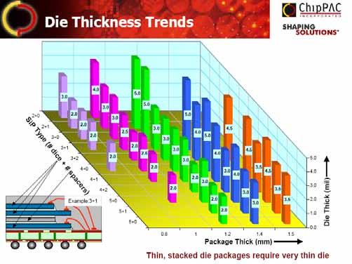
Stack Die CSP Interconnect Challenges Flynn Carson, Glenn Narvaez, HC Choi, and DW Son ChipPAC, Inc.
 Stack Die CSP Interconnect Challenges Flynn Carson, Glenn Narvaez, HC Choi, and DW Son ChipPAC, Inc. IEEE/CPMT Seminar Overview 4 Stacked die Chip Scale Packages (CSPs) enable more device functionality
Chapter 11 Testing, Assembly, and Packaging
 Chapter 11 Testing, Assembly, and Packaging Professor Paul K. Chu Testing The finished wafer is put on a holder and aligned for testing under a microscope Each chip on the wafer is inspected by a multiple-point
Through Glass Via (TGV) Technology for RF Applications
 Technology for RF Applications") Through Glass Via (TGV) Technology for RF Applications C. H. Yun 1, S. Kuramochi 2, and A. B. Shorey 3 1 Qualcomm Technologies, Inc. 5775 Morehouse Dr., San Diego, California 92121, USA Ph: +1-858-651-5449,
Through Glass Via (TGV) Technology for RF Applications C. H. Yun 1, S. Kuramochi 2, and A. B. Shorey 3 1 Qualcomm Technologies, Inc. 5775 Morehouse Dr., San Diego, California 92121, USA Ph: +1-858-651-5449,
3D TSV Micro Cu Column Chip-to-Substrate/Chip Assmbly/Packaging Technology
 3D TSV Micro Cu Column Chip-to-Substrate/Chip Assmbly/Packaging Technology by Seung Wook Yoon, *K. T. Kang, W. K. Choi, * H. T. Lee, Andy C. B. Yong and Pandi C. Marimuthu STATS ChipPAC LTD, 5 Yishun Street
Brief Introduction of Sigurd IC package Assembly
 Brief Introduction of Sigurd IC package Assembly Content Package Development Trend Product Brief Sawing type QFN Representative MEMS Product LGA Light Sensor Proximity Sensor High Yield Capability Low
Compression Molding. Solutions for 3D TSV and other advanced packages as well as cost savings for standard package applications
 Compression Molding Solutions for 3D TSV and other advanced packages as well as cost savings for standard package applications 1. Company Introduction 2. Package Development Trend 3. Compression FFT Molding
TSV MEOL (Mid-End-Of-Line) and its Assembly/Packaging Technology for 3D/2.5D Solutions
 and its Assembly/Packaging Technology for 3D/2.5D Solutions") TSV MEOL (Mid-End-Of-Line) and its Assembly/Packaging Technology for 3D/2.5D Solutions Seung Wook YOON, D.J. Na, *K. T. Kang, W. K. Choi, C.B. Yong, *Y.C. Kim and Pandi C. Marimuthu STATS ChipPAC Ltd.
TSV MEOL (Mid-End-Of-Line) and its Assembly/Packaging Technology for 3D/2.5D Solutions Seung Wook YOON, D.J. Na, *K. T. Kang, W. K. Choi, C.B. Yong, *Y.C. Kim and Pandi C. Marimuthu STATS ChipPAC Ltd.
ULTRON SYSTEMS. Dicing Tape. minitron. elektronik gmbh
 e ULTRON SYSTEMS Dicing Tape minitron elektronik gmbh Overview Dicing Tapes Type Description Page Silikontrennmittelfreie Folien 1003R 1004R 1005R 1007R 1008R 1009R 1011R Blue Plastic Film (PVC), Silicone
First Demonstration of Panel Glass Fan-out (GFO) Packages for High I/O Density and High Frequency Multi-Chip Integration
 Packages for High I/O Density and High Frequency Multi-Chip Integration") First Demonstration of Panel Glass Fan-out (GFO) Packages for High I/O Density and High Frequency Multi-Chip Integration Tailong Shi, Chintan Buch,Vanessa Smet, Yoichiro Sato, Lutz Parthier, Frank Wei
First Demonstration of Panel Glass Fan-out (GFO) Packages for High I/O Density and High Frequency Multi-Chip Integration Tailong Shi, Chintan Buch,Vanessa Smet, Yoichiro Sato, Lutz Parthier, Frank Wei
Two major features of this text
 Two major features of this text Since explanatory materials are systematically made based on subject examination questions, preparation
CHAPTER 11: Testing, Assembly, and Packaging
 Chapter 11 1 CHAPTER 11: Testing, Assembly, and Packaging The previous chapters focus on the fabrication of devices in silicon or the frontend technology. Hundreds of chips can be built on a single wafer,
Challenges of Ultra-thin LGA Package for Fingerprint Sensors
 Challenges of Ultra-thin LGA Package for Fingerprint Sensors Jensen Tsai Deputy Director, SPIL Outline Background Package Features & Challenges Challenges & Solutions Mold Clearance Low Wire Loop Height
Organic Packaging Substrate Workshop Overview
 Organic Packaging Substrate Workshop Overview Organized by: International Electronics Manufacturing Initiative (inemi) Mario A. Bolanos November 17-18, 2009 1 Organic Packaging Substrate Workshop Work
Diverse Lasers Support Key Microelectronic Packaging Tasks
 Diverse Lasers Support Key Microelectronic Packaging Tasks Written by D Muller, R Patzel, G Oulundsen, H Halou, E Rea 23 July 2018 To support more sophisticated and compact tablets, phones, watches and
Lecture: Integration of silicon photonics with electronics. Prepared by Jean-Marc FEDELI CEA-LETI
 Lecture: Integration of silicon photonics with electronics Prepared by Jean-Marc FEDELI CEA-LETI Context The goal is to give optical functionalities to electronics integrated circuit (EIC) The objectives
Review of Wafer Dicing Techniques for Via-Middle Process 3DI/TSV Ultrathin Silicon Device Wafers
 Review of Wafer Dicing Techniques for Via-Middle Process 3DI/TSV Ultrathin Silicon Device Wafers Andy Hooper, Jeff Ehorn, Mike Brand, and Cassie Bassett Micron Technology, Inc. 8000 S. Federal Way, Boise,
ULTRON SYSTEMS. Dicing Tape. minitron. elektronik gmbh
 e ULTRON SYSTEMS Dicing Tape minitron elektronik gmbh Type Description Page Silikontrennmittelfreie Folien 1003R Blue Plastic Film (PVC), Silicone Release Agent-Free, High Strength, 135 µm thick, no backing
POSSUM TM Die Design as a Low Cost 3D Packaging Alternative
 POSSUM TM Die Design as a Low Cost 3D Packaging Alternative The trend toward 3D system integration in a small form factor has accelerated even more with the introduction of smartphones and tablets. Integration
The Smallest Form Factor GPS for Mobile Devices
 2017 IEEE 67th Electronic Components and Technology Conference The Smallest Form Factor GPS for Mobile Devices Eb Andideh 1, Chuck Carpenter 2, Jason Steighner 2, Mike Yore 2, James Tung 1, Lynda Koerber
ASAHI DIAMOND. SILICON PROCESSING TOOLS for SEMICONDUCTORS SEMICONDUCTOR B-52-1
 ASAHI DIAMOND SILICON PROCESSING TOOLS for SEMICONDUCTORS SEMICONDUCTOR B-52-1 Asahi Diamond makes a social foundation. We see electronics and semiconductor products used in various ways in our surroundings.
Advances in X-Ray Technology for Semicon Applications Keith Bryant and Thorsten Rother
 Advances in X-Ray Technology for Semicon Applications Keith Bryant and Thorsten Rother X-Ray Champions, Telspec, Yxlon International Agenda The x-ray tube, the heart of the system Advances in digital detectors
Modeling, Design, and Demonstration of 2.5D Glass Interposers for 16-Channel 28 Gbps Signaling Applications
 Modeling, Design, and Demonstration of 2.5D Glass Interposers for 16-Channel 28 Gbps Signaling Applications Brett Sawyer, Bruce C. Chou, Saumya Gandhi, Jack Mateosky, Venky Sundaram, and Rao Tummala 3D
General Rules for Bonding and Packaging
 General Rules for Bonding and Packaging at the Else Kooi Laboratory 3 CONTENT Rules for assembly at EKL 4 Introduction to assembly 5 Rules for Saw Lane 7 Rules for Chip Size 8 Rules for Bondpads 9 Rules
Application Note AN-1011
 AN-1011 Board Mounting Application Note for 0.800mm Pitch Devices For part numbers IRF6100, IRF6100PBF, IR130CSP, IR130CSPPBF, IR140CSP, IR140CSPPBF, IR1H40CSP, IR1H40CSPPBF By Hazel Schofield and Philip
Electroless Bumping for 300mm Wafers
 Electroless Bumping for 300mm Wafers T. Oppert Internepcon 2006 Tokyo Big Sight, Japan Outline Short Company Profile Electroless Ni/Au Under Bump Metallization UBM for Copper Devices Solder Bumping: Stencil
SAMPLE SLIDES & COURSE OUTLINE. Core Competency In Semiconductor Technology: 2. FABRICATION. Dr. Theodore (Ted) Dellin
 Dellin") & Digging Deeper Devices, Fabrication & Reliability For More Info:.com or email Dellin@ieee.org SAMPLE SLIDES & COURSE OUTLINE In : 2. A Easy, Effective, of How Devices Are.. Recommended for everyone who
& Digging Deeper Devices, Fabrication & Reliability For More Info:.com or email Dellin@ieee.org SAMPLE SLIDES & COURSE OUTLINE In : 2. A Easy, Effective, of How Devices Are.. Recommended for everyone who
An Introduction to Electronics Systems Packaging. Prof. G. V. Mahesh. Department of Electronic Systems Engineering
 An Introduction to Electronics Systems Packaging Prof. G. V. Mahesh Department of Electronic Systems Engineering India Institute of Science, Bangalore Module No. # 02 Lecture No. # 08 Wafer Packaging Packaging
FLIP CHIP LED SOLDER ASSEMBLY
 As originally published in the SMTA Proceedings FLIP CHIP LED SOLDER ASSEMBLY Gyan Dutt, Srinath Himanshu, Nicholas Herrick, Amit Patel and Ranjit Pandher, Ph.D. Alpha Assembly Solutions South Plainfield,
Encapsulated Wafer Level Chip Scale Package (ewlcsp ) for Cost Effective and Robust Solutions in FlexLine
 for Cost Effective and Robust Solutions in FlexLine") Encapsulated Wafer Level Chip Scale Package (ewlcsp ) for Cost Effective and Robust Solutions in FlexLine by Yaojian Lin, Kang Chen, Kian Meng Heng, Linda Chua and *Seung Wook Yoon STATS ChipPAC Ltd. 5
Encapsulated Wafer Level Chip Scale Package (ewlcsp ) for Cost Effective and Robust Solutions in FlexLine by Yaojian Lin, Kang Chen, Kian Meng Heng, Linda Chua and *Seung Wook Yoon STATS ChipPAC Ltd. 5
SHELLCASE-TYPE WAFER-LEVEL PACKAGING SOLUTIONS: RF CHARACTERIZATION AND MODELING
 SHELLCASE-TYPE WAFER-LEVEL PACKAGING SOLUTIONS: RF CHARACTERIZATION AND MODELING M Bartek 1, S M Sinaga 1, G Zilber 2, D Teomin 2, A Polyakov 1, J N Burghartz 1 1 Delft University of Technology, Lab of
An Introduction of Strip Chopping Cut Method to Establish a Robust Strip Based Dicing Process on Tape Dicing Concept
 An Introduction of Strip Chopping Cut Method to Establish a Robust Strip Based Dicing Process on Tape Dicing Concept Ibn Asyura Zainuddin (Author) Discrete Unit Process Development Infineon Technologies
BGA (Ball Grid Array)
") BGA (Ball Grid Array) National Semiconductor Application Note 1126 November 2002 Table of Contents Introduction... 2 Package Overview... 3 PBGA (PLASTIC BGA) CONSTRUCTION... 3 TE-PBGA (THERMALLY ENHANCED
BGA (Ball Grid Array) National Semiconductor Application Note 1126 November 2002 Table of Contents Introduction... 2 Package Overview... 3 PBGA (PLASTIC BGA) CONSTRUCTION... 3 TE-PBGA (THERMALLY ENHANCED
200mm and 300mm Test Patterned Wafers for Bonding Process Applications SKW ASSOCIATES, INC.
 C M P C h a r a c t e r I z a t I o n S o l u t I o n s 200mm and 300mm Test Patterned Wafers for Bonding Process Applications SKW ASSOCIATES, INC. 2920 Scott Blvd., Santa Clara, CA 95054 Tel: 408-919-0094,
MICROELECTRONICS ASSSEMBLY TECHNOLOGIES. The QFN Platform as a Chip Packaging Foundation
 West Coast Luncheon January 15, 2014. PROMEX PROMEX INDUSTRIES INC. MICROELECTRONICS ASSSEMBLY TECHNOLOGIES The QFN Platform as a Chip Packaging Foundation 3075 Oakmead Village Drive Santa Clara CA Ɩ 95051
New wafer level stacking technologies and their applications
 New wafer level stacking technologies and their applications WDoD a new 3D PLUS technology Timothee Dargnies 3D PLUS USA Santa Clara, CA 1 Table of Contents Review of existing wafer level assembly processes
Flexline - A Flexible Manufacturing Method for Wafer Level Packages (Extended Abstract)
") Flexline - A Flexible Manufacturing Method for Wafer Level Packages (Extended Abstract) by Tom Strothmann, *Damien Pricolo, **Seung Wook Yoon, **Yaojian Lin STATS ChipPAC Inc.1711 W Greentree Drive Tempe,
Flexline - A Flexible Manufacturing Method for Wafer Level Packages (Extended Abstract) by Tom Strothmann, *Damien Pricolo, **Seung Wook Yoon, **Yaojian Lin STATS ChipPAC Inc.1711 W Greentree Drive Tempe,
HANA Semiconductor (Ayutthaya) Co. Ltd. Die Design Rule For Assembly Of Plastic Devices
 Co. Ltd. Die Design Rule For Assembly Of Plastic Devices") HANA Semiconductor (Ayutthaya) Co. Ltd. Die Design Rule For Assembly Of Plastic Devices 1.0 PURPOSE : 1.1 To define the rules to be observed to facilitate review of process ability of devices prior to
HANA Semiconductor (Ayutthaya) Co. Ltd. Die Design Rule For Assembly Of Plastic Devices 1.0 PURPOSE : 1.1 To define the rules to be observed to facilitate review of process ability of devices prior to
SESUB - Its Leadership In Embedded Die Packaging Technology
 SESUB - Its Leadership In Embedded Die Packaging Technology Sip Conference China 2018 TDK Corporation ECBC, PAF, SESUB BU Kofu, Japan October 17, 2018 Contents SESUB Introduction SESUB Process SESUB Quality
Semiconductor and LED Markets. Jon Sabol Vice President and General Manager Semiconductor and LED Division
 Semiconductor and LED Markets Jon Sabol Vice President and General Manager Semiconductor and LED Division Semiconductor & LED Investing in Semiconductor and LED $ Millions 300 200 27% CAGR 100 0 * FY06
A Low-cost Through Via Interconnection for ISM WLP
 A Low-cost Through Via Interconnection for ISM WLP Jingli Yuan, Won-Kyu Jeung, Chang-Hyun Lim, Seung-Wook Park, Young-Do Kweon, Sung Yi To cite this version: Jingli Yuan, Won-Kyu Jeung, Chang-Hyun Lim,
Expanding film and process for high efficiency 5 sides protection and FO-WLP fabrication
 2017 IEEE 67th Electronic Components and Technology Conference Expanding film and process for high efficiency 5 sides protection and FO-WLP fabrication Kazutaka Honda, Naoya Suzuki, Toshihisa Nonaka, Hirokazu
450mm and Moore s Law Advanced Packaging Challenges and the Impact of 3D
 450mm and Moore s Law Advanced Packaging Challenges and the Impact of 3D Doug Anberg VP, Technical Marketing Ultratech SOKUDO Lithography Breakfast Forum July 10, 2013 Agenda Next Generation Technology
Dicing Through Hard and Brittle Materials in the Micro Electronic Industry By Gideon Levinson, Dicing Tools Product Manager
 Dicing Through Hard and Brittle Materials in the Micro Electronic Industry By Gideon Levinson, Dicing Tools Product Manager A high percentage of micro electronics dicing applications require dicing completely
Fraunhofer IZM - ASSID
 FRAUNHOFER-INSTITUT FÜR Zuverlässigkeit und Mikrointegration IZM Fraunhofer IZM - ASSID All Silicon System Integration Dresden Heterogeneous 3D Wafer Level System Integration 3D system integration is one
Flexible Hybrid Electronics Fabricated with High-Performance COTS ICs using RTI CircuitFilm TM Technology
 Flexible Hybrid Electronics Fabricated with High-Performance COTS ICs using RTI CircuitFilm TM Technology Scott Goodwin 1, Erik Vick 2 and Dorota Temple 2 1 Micross Advanced Interconnect Technology Micross
EMBEDDED ACTIVE DEVICE PACKAGING TECHNOLOGY FOR REAL DDR2 MEMORY CHIPS
 EMBEDDED ACTIVE DEVICE PACKAGING TECHNOLOGY FOR REAL DDR2 MEMORY CHIPS Yin-Po Hung, Tao-Chih Chang, Ching-Kuan Lee, Yuan-Chang Lee, Jing-Yao Chang, Chao-Kai Hsu, Shu-Man Li, Jui-Hsiung Huang, Fang-Jun
Microsystem Technology for Eddy Current Testing Johannes PAUL, Roland HOLZFÖRSTER
 11th European Conference on Non-Destructive Testing (ECNDT 2014), October 6-10, 2014, Prague, Czech Republic More Info at Open Access Database www.ndt.net/?id=16638 Microsystem Technology for Eddy Current
Innovations Push Package-on-Package Into New Markets. Flynn Carson. STATS ChipPAC Inc Kato Rd Fremont, CA 94538
 Innovations Push Package-on-Package Into New Markets by Flynn Carson STATS ChipPAC Inc. 47400 Kato Rd Fremont, CA 94538 Copyright 2010. Reprinted from Semiconductor International, April 2010. By choosing
Active and passive component embedding into low-cost plastic substrates aimed at smart system applications
 Active and passive component embedding into low-cost plastic substrates aimed at smart system applications Maarten Cauwe 1, Bjorn Vandecasteele 1, Johan De Baets 1, Jeroen van den Brand 2, Roel Kusters
NEW PACKAGING AND INTERCONNECT TECHNOLOGIES FOR ULTRA THIN CHIPS
 NEW PACKAGING AND INTERCONNECT TECHNOLOGIES FOR ULTRA THIN CHIPS Christine Kallmayer and Rolf Aschenbrenner Fraunhofer IZM Berlin, Germany kallmayer@izm.fhg.de Julian Haberland and Herbert Reichl Technical
Design and Development of True-CSP
 Design and Development of True-CSP *Kolan Ravi Kanth, Francis K.S. Poh, B.K. Lim, Desmond Y.R. Chong, Anthony Sun, H.B. Tan United Test & Assembly Center Ltd (UTAC) 5 Serangoon North Ave 5, Singapore 554916
The Future of Packaging ~ Advanced System Integration
 The Future of Packaging ~ Advanced System Integration Enabling a Microelectronic World R. Huemoeller SVP, Adv. Product / Platform Develop June 2013 Product Segments End Market % Share Summary 2 New Product
Advanced Packaging Equipment Solder Jetting & Laser Bonding
 Advanced Packaging Equipment Solder Jetting & Laser Bonding www.pactech.comw.pactech.com PacTech Packaging Technologies Pioneering in laser solder jetting technologies since 1995 Our mission is to reshape
Laser MicroJet Technology. Cool Laser Machining.
 Laser MicroJet Technology Cool Laser Machining www.synova.ch Synova S.A., headquartered in Duillier, Switzerland, manufactures leading-edge laser cutting systems since 1997 that incorporate the proprietary
Chapter 7 Introduction to 3D Integration Technology using TSV
 Chapter 7 Introduction to 3D Integration Technology using TSV Jin-Fu Li Department of Electrical Engineering National Central University Jungli, Taiwan Outline Why 3D Integration An Exemplary TSV Process
سمینار درس تئوری و تکنولوژی ساخت
 نام خدا به 1 سمینار درس تئوری و تکنولوژی ساخت Wire Bonding استاد : جناب آقای محمدنژاد دکتر اردیبهشت 93 2 3 Content IC interconnection technologies Whats wirebonding Wire Bonding Processes Thermosonic Wirebond
New Approaches to Develop a Scalable 3D IC Assembly Method
 New Approaches to Develop a Scalable 3D IC Assembly Method Charles G. Woychik Ph.D. Sangil Lee, Ph.D., Scott McGrath, Eric Tosaya and Sitaram Arkalgud Ph.D. Invensas Corporation 3025 Orchard Parkway San
Advanced High-Density Interconnection Technology
 Advanced High-Density Interconnection Technology Osamu Nakao 1 This report introduces Fujikura s all-polyimide IVH (interstitial Via Hole)-multi-layer circuit boards and device-embedding technology. Employing
Okamoto Machine Tool Works, LTD. June 22, th SEMATECH Symposium Japan 1
 Okamoto Machine Tool Works, LTD 1 Contents Solutions for TSV Wafer Thinning Process (Front Side Via) TSV Wafer Thinning Challenges Process Improvement (4-years Development) TSV Wafer Thinning Tool (TSV300)
Flip Chip Bonding Using Sony Anisotropic Conductive Film (ACF) FP1526Y
 FP1526Y") Flip Chip Bonding Using Sony Anisotropic Conductive Film (ACF) FP1526Y Purpose: Author: Rekha S. Pai (07/29/03) To use ACF as an interconnection method for attaching dice to substrates. Direct electrical
Flip Chip Bonding Using Sony Anisotropic Conductive Film (ACF) FP1526Y Purpose: Author: Rekha S. Pai (07/29/03) To use ACF as an interconnection method for attaching dice to substrates. Direct electrical
2016 Substrate & Package Technology Workshop Highlight
 2016 Substrate & Package Technology Workshop Highlight Webinar July 13, 2016 Theme of the Workshop inemi roadmap and Technical plan highlighted that year 2015 was the year entering critical package technology
!"#$"%&' ()#*+,-+.&/0(
#*+,-+.&/0(") !"#$"%&' ()#*+,-+.&/0( Multi Chip Modules (MCM) or Multi chip packaging Industry s first MCM from IBM. Generally MCMs are horizontal or two-dimensional modules. Defined as a single unit containing two
!"#$"%&' ()#*+,-+.&/0( Multi Chip Modules (MCM) or Multi chip packaging Industry s first MCM from IBM. Generally MCMs are horizontal or two-dimensional modules. Defined as a single unit containing two
2.5D Platform (Examples of products produced to date are shown here to demonstrate Amkor's production capabilities)
") Wafer Finishing & Flip Chip Stacking interconnects have emerged to serve a wide range of 2.5D- & 3D- packaging applications and architectures that demand very high performance and functionality at the
Wafer Finishing & Flip Chip Stacking interconnects have emerged to serve a wide range of 2.5D- & 3D- packaging applications and architectures that demand very high performance and functionality at the
Optical Characterization and Defect Inspection for 3D Stacked IC Technology
 Minapad 2014, May 21 22th, Grenoble; France Optical Characterization and Defect Inspection for 3D Stacked IC Technology J.Ph.Piel, G.Fresquet, S.Perrot, Y.Randle, D.Lebellego, S.Petitgrand, G.Ribette FOGALE
Flip chip Assembly with Sub-micron 3D Re-alignment via Solder Surface Tension
 Flip chip Assembly with Sub-micron 3D Re-alignment via Solder Surface Tension Jae-Woong Nah*, Yves Martin, Swetha Kamlapurkar, Sebastian Engelmann, Robert L. Bruce, and Tymon Barwicz IBM T. J. Watson Research
Embedded Si Fan Out: A Low Cost Wafer Level Packaging Technology Without Molding and De-bonding Processes
 2017 IEEE 67th Electronic Components and Technology Conference Embedded Si Fan Out: A Low Cost Wafer Level Packaging Technology Without Molding and De-bonding Processes Daquan Yu*, Zhenrui Huang, Zhiyi
Enabling Areal Density Growth
 Shrinking the Magnetic Spacing for Advanced PMR Heads Diskcon Asia 2007 Enabling Areal Density Growth Shrinking the magnetic spacing remains one of the biggest levers for areal density growth! Areal Density
Tape Automated Bonding
 Tape Automated Bonding Introduction TAB evolved from the minimod project begun at General Electric in 1965, and the term Tape Automated Bonding was coined by Gerard Dehaine of Honeywell Bull in 1971. The
Integration of 3D detector systems
 Integration of 3D detector systems Piet De Moor Introduction Evolution in radiation detection/imaging: single pixel linear array 2D array increase in resolution = decrease in pitch (down to few um) = thanks
Technology development for a flexible, low-cost backplane for lighting applications
 IMAPS-Benelux Spring Event 2014 Technology development for a flexible, low-cost backplane for lighting applications M. Cauwe 1, A. Sridhar 2, T. Sterken 1 1 imec - Cmst, Technologiepark, Zwijnaarde, Belgium
PANEL LEVEL PACKAGING A MANUFACTURING SOLUTION FOR COST-EFFECTIVE SYSTEMS
 PANEL LEVEL PACKAGING A MANUFACTURING SOLUTION FOR COST-EFFECTIVE SYSTEMS R. Aschenbrenner, K.-F. Becker, T. Braun, and A. Ostmann Fraunhofer Institute for Reliability and Microintegration Berlin, Germany
Copyright 2009 Year IEEE. Reprinted from 2009 Electronic Components and Technology Conference. Such permission of the IEEE does not in any way imply
 Copyright 2009 Year IEEE. Reprinted from 2009 Electronic Components and Technology Conference. Such permission of the IEEE does not in any way imply IEEE endorsement of any of Institute of Microelectronics
PERSPECTIVES FOR DISRUPTIVE 200MM/8-INCH GAN POWER DEVICE AND GAN-IC TECHNOLOGY DR. DENIS MARCON SR. BUSINESS DEVELOPMENT MANAGER
 PERSPECTIVES FOR DISRUPTIVE 200MM/8-INCH GAN POWER DEVICE AND GAN-IC TECHNOLOGY DR. DENIS MARCON SR. BUSINESS DEVELOPMENT MANAGER What I will show you today 200mm/8-inch GaN-on-Si e-mode/normally-off technology
Wafer-scale 3D integration of silicon-on-insulator RF amplifiers
 Wafer-scale integration of silicon-on-insulator RF amplifiers The MIT Faculty has made this article openly available. Please share how this access benefits you. Your story matters. Citation As Published
Nanometer Technologies: Where Design and Manufacturing Converge. Walden C. Rhines CHAIRMAN & CEO
 Nanometer Technologies: Where Design and Manufacturing Converge Walden C. Rhines CHAIRMAN & CEO Nanometer Technologies: Where Design and Manufacturing Converge Nanometer technologies make designers aware
TTC-1002 Thermal Test Chip Applications Manual
 COVER TTC-1002 Thermal Test Chip Applications Manual Thermal Engineering Associates, Inc. 3287 Kifer Road Santa Clara, CA 95051 USA 650-961-5900 www.thermengr.com CONTENTS Section 1 Section 2 Section
Applications and opportunities of AM in Diebond equipment
 2018, March 22 Applications and opportunities of AM in Diebond equipment Patrick Houben Ralph Huijbers Content Nexperia introduction Department ITEC Pick and place machine (ADAT3) AM example 1 : Bondhead
Plan Optik AG. Plan Optik AG PRODUCT CATALOGUE
 Plan Optik AG Plan Optik AG PRODUCT CATALOGUE 2 In order to service the high demand of wafers more quickly, Plan Optik provides off the shelf products in sizes from 2 up to 300mm diameter. Therefore Plan
Electronic supplementary material
 Electronic supplementary material Three-dimensionally Deformable, Highly Stretchable, Permeable, Durable and Washable Fabric Circuit Boards Qiao Li 1, and Xiao Ming Tao 1,2 * 1 Institute of Textiles and
450mm patterning out of darkness Backend Process Exposure Tool SOKUDO Lithography Breakfast Forum July 10, 2013 Doug Shelton Canon USA Inc.
 450mm patterning out of darkness Backend Process Exposure Tool SOKUDO Lithography Breakfast Forum 2013 July 10, 2013 Doug Shelton Canon USA Inc. Introduction Half Pitch [nm] 2013 2014 2015 2016 2017 2018
B. Flip-Chip Technology
 B. Flip-Chip Technology B1. Level 1. Introduction to Flip-Chip techniques B1.1 Why flip-chip? In the development of packaging of electronics the aim is to lower cost, increase the packaging density, improve
Capabilities of Flip Chip Defects Inspection Method by Using Laser Techniques
 Capabilities of Flip Chip Defects Inspection Method by Using Laser Techniques Sheng Liu and I. Charles Ume* School of Mechanical Engineering Georgia Institute of Technology Atlanta, Georgia 3332 (44) 894-7411(P)
Introduction of IMS Technology for Advanced Solder Bumping on Wafers / Laminates
 Introduction of IMS Technology for Advanced Solder Bumping on Wafers / Laminates Science & Technology IBM Research Tokyo Yasumitsu Orii, PhD Senju Metal Industry Co.,TW Deputy General Manager Lewis Huang
Ultra-Thin, Highly Flexible Cables and Interconnections for Low and High Frequencies
 Ultra-Thin, Highly Flexible Cables and Interconnections for Low and High Frequencies Hans Burkard a, Tobias Lamprecht b, Thomas Morf b, Bert Jan Offrein b, Josef Link a a Hightec MC AG, Fabrikstrasse,
Disruptive Developments for Advanced Die Attach to Tackle the Challenges of Heterogeneous Integration
 Disruptive Developments for Advanced Die Attach to Tackle the Challenges of Heterogeneous Integration Hugo Pristauz & Andreas Mayr, Besi Austria presented by: Stefan Behler, Besi Switzerland ECTC 2018