A transparent, conformable, active multielectrode array using organic electrochemical transistors
|
|
|
- Mildred Fitzgerald
- 5 years ago
- Views:
Transcription
1 Supplementary Information A transparent, conformable, active multielectrode array using organic electrochemical transistors Wonryung Lee a, Dongmin Kim a,b, Naoji Matsuhisa a, Masae Nagase a,b, Masaki Sekino a,b, George G Malliaras c, Tomoyuki Yokota a,b, and Takao Someya a,b,d,1 a Department of Electrical Engineering and Information Systems, The University of Tokyo, Hongo, Bunkyo-ku, Tokyo , Japan b Exploratory Research for Advanced Technology (ERATO), Japan Science and Technology Agency (JST), Hongo, Bunkyo-ku, Tokyo , Japan c Ecole Nationale Supérieure des Mines, 880, route de Mimet, Gardanne, France d Thin-Film Device Laboratory & Center for Emergent Matter Science (CEMS), RIKEN, 2-1 Hirosawa, Wako, Saitama , Japan


2 Figure S1: Fabrication process for manufacturing the electrophysiology array with transparent organic electrochemical transistors (OECTs).
3 Figure S2: Correlation between the conductance and transparency of the Au grid, which is obtained by calculation. (ρ = Ωm, Tc = (p w) 2 / p 2 ).
 of (A) transparent OECT")
.")
4 Figure S3: Microscope image (Scale bar: 1 mm) of (A) transparent OECT and (B) nontransparent OECT with a magnified view (Scale bar: 70 μm).
. (C) Ids fluctuation when 10 mv amplitude of sinusoidal Vgs was applied.")
5 Figure S4: The bandwidth of the transparent OECT (W/L = 70 µm/20 µm) (A) The schematic of the measurement set-up (B) The I V curve of the transparent OECT. gm was 3.5 ms (Vg = 0 V). (C) Ids fluctuation when 10 mv amplitude of sinusoidal Vgs was applied. (D) gm of transparent OECT at various frequencies.
 Schematic of experimental setting for evaluation of leakage current (B) The")
6 Figure S5: Leakage current of 1.2-μm-thick SU-8 with DC bias in 37 degrees PBS (A) Schematic of experimental setting for evaluation of leakage current (B) The leakage current after dipping 0 hr and 24 hrs. (C) The time-leakage current curve at 0.6V bias voltage.
 and gate leakage current (Ig) after dipping 0 hr and 24 hrs. (C) The time-ig curve when the drain voltage was 0.")
7 Figure S6: The long-term gate leakage current of OECTs in 37 degrees PBS (A) Schematic of experimental setting for evaluation of gate leakage current of OECTs (B) The drain current (Id) and gate leakage current (Ig) after dipping 0 hr and 24 hrs. (C) The time-ig curve when the drain voltage was 0.6V and the gate voltage was 0V.
8 Figure S7: The Ids Vg curve of the transistor for simulation of Figure S7, S8, S9. The p-type transistor was set to Vth = 1 V and gm = 0.6 ms. PSpice (student version 9.1) was used for the simulation.

9
10 Figure S8: Crosstalk evaluation when unselected data/scan lines are grounded and floating. (A) Concepts that describe how crosstalk is avoided by grounding the unselected data/scan lines. No voltage difference was applied to the OECTs on the unselected data lines, resulting in no current in these OECTs and no crosstalk (Is = I2). (B) Concepts that describe how crosstalk happens when the unselected data/scan lines are open. Voltage differences are applied to OECTs on the unselected data lines, resulting in currents in these OECTs and crosstalk (Is = I1 + I2). (C) Circuit schematic to evaluate crosstalk current when the unselected data/scan lines are grounded. (D) The simulation result of currents from each transistor in C. Except I4~6 (selected data line), the current was 0. I5 showed current fluctuation of 3 Hz, and was identical as Is. (E) Circuit schematic to evaluate crosstalk current when the unselected data/scan lines are open. (F) The simulation result of currents from each transistor in E. Currents were observed in I1,3,7,9 and I2,4,6,8 because the voltage difference is induced to the corresponding OECTs. Consequently, Is was mixed (I2 + I5 + I8).

 and open (C,D). (A,C) Circuit schematics.")
11 Figure S9: The crosstalk simulation with different frequency inputs. Signals with frequencies of 2, 3, and 5 Hz were applied to 3 different OECTs (M21, M22, and M23 respectively), and the current in one of the scan lines was compared when unselected data/scan lines are grounded (A, B) and open (C,D). (A,C) Circuit schematics. (B,D) Simulation results of Is.


12
13 Figure S10: Simulation data when the array was multiplexed. (A) Circuit schematic of the OECT array when it was multiplexed. The output signal of Is1, Is2, Is3 was shown in the bottom of circuit schematic, while the gate voltages (Vg13, Vg21, Vg22, Vg31, Vg32) of amplitude 100 mv were applied to the transistors (M13, M21, M22, M31,M32). (B) The output signal of Id1s1~Id3s3, which is separated by the timing of the applied pulse (V1, V2, V3), while the gate voltages (Vg13, Vg21, Vg22, Vg31,Vg32) of amplitude 100 mv were applied to the transistors (M13, M21, M22, M31,M32). The separated current was named by the number of scan lines (S1, S2, S3) and data lines (D1, D2, D3).


14
15 Figure S11: Experimental evaluation of crosstalk in an OECT array. (A) Photographic image of the 3 3 OECT array. Scale bar: 1 mm (B) Magnified microscope view of a cell in the array. Scale bar: 100 μm (C) Circuit schematic for evaluating crosstalk in a data line. Different gate voltage inputs were applied to OECTs on the same data line. (D) Measured currents in each of the scan lines. Outputs with different frequencies were clearly recorded in each scan line. (E) Circuit schematic for evaluating crosstalk in a scan line. Different gate voltage inputs were applied to OECTs on the same scan line. (F) Measured currents when voltages in the data lines were switched. Signals with specific frequencies were obtained when voltage was applied to the corresponding data line.

16
17 Figure S12: Simulation data when the array was multiplexed with high load resistance (RL). (A) Circuit schematic of the OECT array when it was multiplexed with 1 kω of RL. The gate voltages (Vg13, Vg21, Vg22, Vg31, Vg32) of amplitude 100 mv were applied to the transistors (M13, M21, M22, M31,M32) which is same as Fig S10(A). (B) The output signal of Vd1s1~Vd3s3, which is separated by the timing of the applied pulse (V1, V2, V3), while the gate voltages (Vg13, Vg21, Vg22, Vg31, Vg32) of the amplitude of 100 mv were applied to the transistors (M13, M21, M22, M31,M32). The separated current was named by the number of scan lines (S1, S2, S3) and data lines (D1, D2, D3).

18
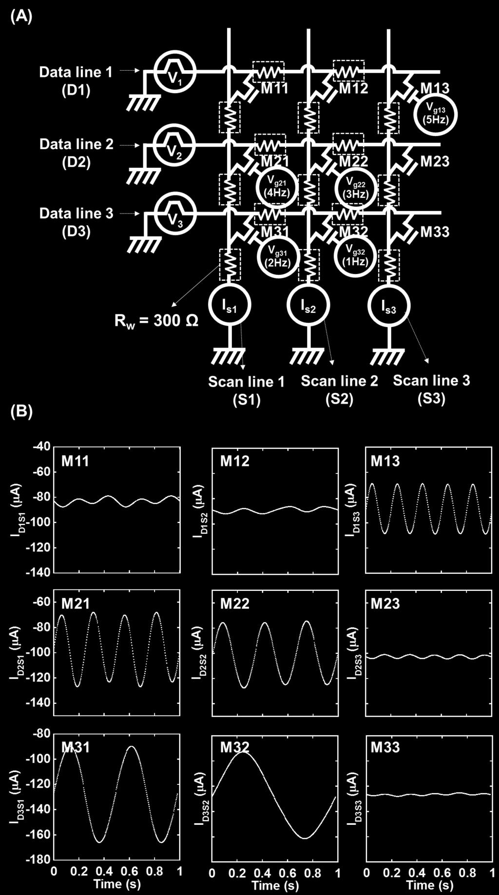
19 Figure S13: Simulation data when the array was multiplexed with 300Ω of wire resistance (Rw). (A) Circuit schematic of the OECT array when it was multiplexed with 300Ω of Rw. The gate voltages (Vg13, Vg21, Vg22, Vg31, Vg32) of amplitude 100 mv were applied to the transistors (M13, M21, M22, M31,M32) which is same as Fig S10(A). (B) The output signal of Vd1s1~Vd3s3, which is separated by the timing of the applied pulse (V1, V2, V3), while the gate voltages (Vg13, Vg21, Vg22, Vg31, Vg32) of the amplitude of 100 mv were applied to the transistors (M13, M21, M22, M31,M32). The separated current was named by the number of scan lines (S1, S2, S3) and data lines (D1, D2, D3).
20 Figure S14: Continuous current measurement of the transparent OECT (Vds = 0.6 V), which is directly stimulated by light through an optical fiber (with diameter 500 µm) on its channel at 5 Hz and a duration of 5 ms during an in-vivo experiment. It was conducted on the brain surface of living and dead optogenetic rats. The data was filtered at the frequency of more than 1 khz. The RMS was 0.02 µa. No clear light artefact was observed for the control data.
21 Figure S15: The site impedance of the transparent OECT (W/L = 70 µm/20 µm). The site impedance at 1 khz was 10 kω.
In vivo recordings of brain activity using organic transistors
 Supplementary Information In vivo recordings of brain activity using organic transistors Dion Khodagholy 1, Thomas Doublet 1,2,3,4, Pascale Quilichini 2,3, Moshe Gurfinkel 1, Pierre Leleux 1,2,3,4, Antoine
SUPPLEMENTARY INFORMATION
 A transparent bending-insensitive pressure sensor Sungwon Lee 1,2, Amir Reuveny 1,2, Jonathan Reeder 1#, Sunghoon Lee 1,2, Hanbit Jin 1,2, Qihan Liu 5, Tomoyuki Yokota 1,2, Tsuyoshi Sekitani 1,2,3, Takashi
A large-area wireless power transmission sheet using printed organic. transistors and plastic MEMS switches
 Supplementary Information A large-area wireless power transmission sheet using printed organic transistors and plastic MEMS switches Tsuyoshi Sekitani 1, Makoto Takamiya 2, Yoshiaki Noguchi 1, Shintaro
UNIVERSITY OF NORTH CAROLINA AT CHARLOTTE Department of Electrical and Computer Engineering
 UNIVERSITY OF NORTH CAROLINA AT CHARLOTTE Department of Electrical and Computer Engineering EXPERIMENT 8 MOSFET AMPLIFIER CONFIGURATIONS AND INPUT/OUTPUT IMPEDANCE OBJECTIVES The purpose of this experiment
UNIVERSITY OF NORTH CAROLINA AT CHARLOTTE. Department of Electrical and Computer Engineering
 UNIVERSITY OF NORTH CAROLINA AT CHARLOTTE Department of Electrical and Computer Engineering Experiment No. 9 - MOSFET Amplifier Configurations Overview: The purpose of this experiment is to familiarize
University of Pittsburgh
 University of Pittsburgh Experiment #4 Lab Report MOSFET Amplifiers and Current Mirrors Submission Date: 07/03/2018 Instructors: Dr. Ahmed Dallal Shangqian Gao Submitted By: Nick Haver & Alex Williams
XYZ Stage. Surface Profile Image. Generator. Servo System. Driving Signal. Scanning Data. Contact Signal. Probe. Workpiece.
 Jpn. J. Appl. Phys. Vol. 40 (2001) pp. 3646 3651 Part 1, No. 5B, May 2001 c 2001 The Japan Society of Applied Physics Estimation of Resolution and Contact Force of a Longitudinally Vibrating Touch Probe
ENEE 307 Laboratory#2 (n-mosfet, p-mosfet, and a single n-mosfet amplifier in the common source configuration)
") Revised 2/16/2007 ENEE 307 Laboratory#2 (n-mosfet, p-mosfet, and a single n-mosfet amplifier in the common source configuration) *NOTE: The text mentioned below refers to the Sedra/Smith, 5th edition.
Revised 2/16/2007 ENEE 307 Laboratory#2 (n-mosfet, p-mosfet, and a single n-mosfet amplifier in the common source configuration) *NOTE: The text mentioned below refers to the Sedra/Smith, 5th edition.
LAB 4 : FET AMPLIFIERS
 LEARNING OUTCOME: LAB 4 : FET AMPLIFIERS In this lab, students design and implement single-stage FET amplifiers and explore the frequency response of the real amplifiers. Breadboard and the Analog Discovery
The George Washington University School of Engineering and Applied Science Department of Electrical and Computer Engineering ECE 20 - LAB
 The George Washington University School of Engineering and Applied Science Department of Electrical and Computer Engineering ECE 20 - LAB Experiment # 11 MOSFET Amplifiers testing and designing Equipment:
EE 230 Lab Lab 9. Prior to Lab
 MOS transistor characteristics This week we look at some MOS transistor characteristics and circuits. Most of the measurements will be done with our usual lab equipment, but we will also use the parameter
Circular Dichroism Microscopy Free from Commingling Linear Dichroism via Discretely Modulated Circular Polarization
 Supplementary information Circular Dichroism Microscopy Free from Commingling Linear Dichroism via Discretely Modulated Circular Polarization Tetsuya Narushima AB and Hiromi Okamoto A* A Institute for
SG2525A SG3525A REGULATING PULSE WIDTH MODULATORS
 SG2525A SG3525A REGULATING PULSE WIDTH MODULATORS 8 TO 35 V OPERATION 5.1 V REFERENCE TRIMMED TO ± 1 % 100 Hz TO 500 KHz OSCILLATOR RANGE SEPARATE OSCILLATOR SYNC TERMINAL ADJUSTABLE DEADTIME CONTROL INTERNAL
Spectrally Selective Photocapacitance Modulation in Plasmonic Nanochannels for Infrared Imaging
 Supporting Information Spectrally Selective Photocapacitance Modulation in Plasmonic Nanochannels for Infrared Imaging Ya-Lun Ho, Li-Chung Huang, and Jean-Jacques Delaunay* Department of Mechanical Engineering,
HI-201HS. High Speed Quad SPST CMOS Analog Switch
 SEMICONDUCTOR HI-HS December 99 Features Fast Switching Times, N = ns, FF = ns Low ON Resistance of Ω Pin Compatible with Standard HI- Wide Analog Voltage Range (±V Supplies) of ±V Low Charge Injection
Supplementary Materials for
 advances.sciencemag.org/cgi/content/full/2/1/e1501101/dc1 Supplementary Materials for A wearable multiplexed silicon nonvolatile memory array using nanocrystal charge confinement Jaemin Kim, Donghee Son,
Lab 6: MOSFET AMPLIFIER
 Lab 6: MOSFET AMPLIFIER NOTE: This is a "take home" lab. You are expected to do the lab on your own time (still working with your lab partner) and then submit your lab reports. Lab instructors will be
Supplementary Materials for
 advances.sciencemag.org/cgi/content/full/2/6/e1501326/dc1 Supplementary Materials for Organic core-sheath nanowire artificial synapses with femtojoule energy consumption Wentao Xu, Sung-Yong Min, Hyunsang
TDA W Hi-Fi AUDIO POWER AMPLIFIER
 32W Hi-Fi AUDIO POWER AMPLIFIER HIGH OUTPUT POWER (50W MUSIC POWER IEC 268.3 RULES) HIGH OPERATING SUPPLY VOLTAGE (50V) SINGLE OR SPLIT SUPPLY OPERATIONS VERY LOW DISTORTION SHORT CIRCUIT PROTECTION (OUT
K-BAND HARMONIC DIELECTRIC RESONATOR OS- CILLATOR USING PARALLEL FEEDBACK STRUC- TURE
 Progress In Electromagnetics Research Letters, Vol. 34, 83 90, 2012 K-BAND HARMONIC DIELECTRIC RESONATOR OS- CILLATOR USING PARALLEL FEEDBACK STRUC- TURE Y. C. Du *, Z. X. Tang, B. Zhang, and P. Su School
STK4362. AF Power Amplifier (10W + 10W min, THD = 1.0%)
") Ordering number: EN 1229C Thick Film Hybrid IC AF Power Amplifier (10W + 10W min, THD = 1.0%) Features Package Dimensions Capable of guaranteeing substrate temperature 125 C, thereby reducing heat sink.
Ordering number: EN 1229C Thick Film Hybrid IC AF Power Amplifier (10W + 10W min, THD = 1.0%) Features Package Dimensions Capable of guaranteeing substrate temperature 125 C, thereby reducing heat sink.
STK4332. AF Power Amplifier (5W + 5W min, THD = 1.0%)
") Ordering number: EN 1227C Thick Film Hybrid IC STK4332 AF Power Amplifier (5W + 5W min, THD = 1.0%) Features Package Dimensions Small and slim package with 25.5 mm height. Capable of guaranteeing substrate
Ordering number: EN 1227C Thick Film Hybrid IC STK4332 AF Power Amplifier (5W + 5W min, THD = 1.0%) Features Package Dimensions Small and slim package with 25.5 mm height. Capable of guaranteeing substrate
TL072 TL072A - TL072B
 A - B LOW NOISE J-FET DUAL OPERATIONAL AMPLIFIERS WIDE COMMON-MODE (UP TO V + CC ) AND DIFFERENTIAL VOLTAGE RANGE LOW INPUT BIAS AND OFFSET CURRENT LOW NOISE e n = 15nV/ Hz (typ) OUTPUT SHORT-CIRCUIT PROTECTION
Experimental Studies of Vulnerabilities in Devices and On-Chip Protection
 Acknowledgements: Support by the AFOSR-MURI Program is gratefully acknowledged 6/8/02 Experimental Studies of Vulnerabilities in Devices and On-Chip Protection Agis A. Iliadis Electrical and Computer Engineering
TL082 TL082A - TL082B
 TL082 TL082A - TL082B GENERAL PURPOSE J-FET DUAL OPERATIONAL AMPLIFIERS WIDE COMMON-MODE (UP TO V + CC ) AND DIFFERENTIAL VOLTAGE RANGE LOW INPUT BIAS AND OFFSET CURRENT OUTPUT SHORT-CIRCUIT PROTECTION
Supplementary Information
 Supplementary Information Synthesis of hybrid nanowire arrays and their application as high power supercapacitor electrodes M. M. Shaijumon, F. S. Ou, L. Ci, and P. M. Ajayan * Department of Mechanical
Ultra-short pulse ECM using electrostatic induction feeding method
 Available online at www.sciencedirect.com Procedia CIRP 6 (213 ) 39 394 The Seventeenth CIRP Conference on Electro Physical and Chemical Machining (ISEM) Ultra-short pulse ECM using electrostatic induction
Well we know that the battery Vcc must be 9V, so that is taken care of.
 HW 4 For the following problems assume a 9Volt battery available. 1. (50 points, BJT CE design) a) Design a common emitter amplifier using a 2N3904 transistor for a voltage gain of Av=-10 with the collector
TL081 TL081A - TL081B
 TL081 TL081A - TL081B GENERAL PURPOSE J-FET SINGLE OPERATIONAL AMPLIFIERS WIDE COMMON-MODE (UP TO V + CC ) AND DIFFERENTIAL VOLTAGE RANGE LOW INPUT BIAS AND OFFSET CURRENT OUTPUT SHORT-CIRCUIT PROTECTION
An impedance-based integrated biosensor for suspended DNA characterisation
 An impedance-based integrated biosensor for suspended DNA characterisation Hanbin Ma, Richard W.R. Wallbank, Reza Chaji, Jiahao Li, Yuji Suzuki, Chris Jiggins and Arokia Nathan Supplementary Item Title
Objectives The purpose of this lab is build and analyze Differential amplifiers based on NMOS transistors (or NPN transistors).
.") 1 Lab 03: Differential Amplifiers (MOSFET) (20 points) NOTE: 1) Please use the basic current mirror from Lab01 for the second part of the lab (Fig. 3). 2) You can use the same chip as the basic current
1 Lab 03: Differential Amplifiers (MOSFET) (20 points) NOTE: 1) Please use the basic current mirror from Lab01 for the second part of the lab (Fig. 3). 2) You can use the same chip as the basic current
STK4026V. AF Power Amplifier (Split Power Supply) (25W min, THD = 0.08%)
 (25W min, THD = 0.08%)") Ordering number: 2131B Thick Film Hybrid IC STK4026V AF Power Amplifier (Split Power Supply) (25W min, THD = 0.08%) Features Small-sized package permitting audio sets to be made slimmer (up to 70W) The
Ordering number: 2131B Thick Film Hybrid IC STK4026V AF Power Amplifier (Split Power Supply) (25W min, THD = 0.08%) Features Small-sized package permitting audio sets to be made slimmer (up to 70W) The
LF147 - LF247 LF347 WIDE BANDWIDTH QUAD J-FET OPERATIONAL AMPLIFIERS
 LF147 - LF247 LF347 WIDE BANDWIDTH QUAD J-FET OPERATIONAL AMPLIFIERS LOW POWER CONSUMPTION WIDE COMMON-MODE (UP TO V + CC ) AND DIFFERENTIAL VOLTAGE RANGE LOW INPUT BIAS AND OFFSET CURRENT OUTPUT SHORT-CIRCUIT
unit: mm 4033 THD = 1.0%, Po (2) f = 30Hz to 20kHz
 f = 30Hz to 20kHz") Ordering number: EN2885A Thick Film Hybrid IC STK4432 AF Power Amplifier (25W + 25W min, THD = 1.0%) Features Package Dimensions Small and slim package with 31 mm height Pin compatible with STK430 series
Ordering number: EN2885A Thick Film Hybrid IC STK4432 AF Power Amplifier (25W + 25W min, THD = 1.0%) Features Package Dimensions Small and slim package with 31 mm height Pin compatible with STK430 series
8. Characteristics of Field Effect Transistor (MOSFET)
") 1 8. Characteristics of Field Effect Transistor (MOSFET) 8.1. Objectives The purpose of this experiment is to measure input and output characteristics of n-channel and p- channel field effect transistors
1 8. Characteristics of Field Effect Transistor (MOSFET) 8.1. Objectives The purpose of this experiment is to measure input and output characteristics of n-channel and p- channel field effect transistors
LF147 - LF247 LF347 WIDE BANDWIDTH QUAD J-FET OPERATIONAL AMPLIFIERS
 LF147 - LF247 LF347 WIDE BANDWIDTH QUAD J-FET OPERATIONAL AMPLIFIERS LOW POWER CONSUMPTION WIDE COMMON-MODE (UP TO V + CC ) AND DIFFERENTIAL VOLTAGE RANGE LOW INPUT BIAS AND OFFSET CURRENT OUTPUT SHORT-CIRCUIT
1. The simple, one transistor current source
 1. The simple, one transistor current source The test schematic (srs-simpla-mos.asc): 1. Design the NMOS source for a 40µA output current and the minimum allowed output voltage V omin =50mV. The design
DATA SHEET N-CHANNEL SILICON JUNCTION FIELD EFFECT TRANSISTOR FOR IMPEDANCE CONVERTER OF ECM
 DATA SHEET JUNCTION FIELD EFFECT TRANSISTOR N-CHANNEL SILICON JUNCTION FIELD EFFECT TRANSISTOR FOR IMPEDANCE CONVERTER OF ECM DESCRIPTION The is suitable for converter of ECM. General-purpose product.
Paper-1 (Circuit Analysis) UNIT-I
 UNIT-I") Paper-1 (Circuit Analysis) UNIT-I AC Fundamentals & Kirchhoff s Current and Voltage Laws 1. Explain how a sinusoidal signal can be generated and give the significance of each term in the equation? 2. Define
Paper-1 (Circuit Analysis) UNIT-I AC Fundamentals & Kirchhoff s Current and Voltage Laws 1. Explain how a sinusoidal signal can be generated and give the significance of each term in the equation? 2. Define
SUPPLEMENTARY INFORMATION
 Induction of coherent magnetization switching in a few atomic layers of FeCo using voltage pulses Yoichi Shiota 1, Takayuki Nozaki 1, 2,, Frédéric Bonell 1, Shinichi Murakami 1,2, Teruya Shinjo 1, and
LM13600 Dual Operational Transconductance Amplifiers with Linearizing Diodes and Buffers
 LM13600 Dual Operational Transconductance Amplifiers with Linearizing Diodes and Buffers General Description The LM13600 series consists of two current controlled transconductance amplifiers each with
TL084 TL084A - TL084B
 A B GENERAL PURPOSE JFET QUAD OPERATIONAL AMPLIFIERS WIDE COMMONMODE (UP TO V + CC ) AND DIFFERENTIAL VOLTAGE RANGE LOW INPUT BIAS AND OFFSET CURRENT OUTPUT SHORTCIRCUIT PROTECTION HIGH INPUT IMPEDANCE
Redefining Measurement ID101 OEM Visible Photon Counter
 Redefining Measurement ID OEM Visible Photon Counter Miniature Photon Counter for OEM Applications Intended for large-volume OEM applications, the ID is the smallest, most reliable and most efficient single-photon
HI-201HS. Features. High Speed, Quad SPST, CMOS Analog Switch. Applications. Ordering Information. Pinout (Switches Shown For Logic 1 Input) FN3123.
 FN3123.") HI-HS Data Sheet September 4 FN.4 High Speed, Quad SPST, CMOS Analog Switch The HI-HS is a monolithic CMOS Analog Switch featuring very fast switching speeds and low ON resistance. The integrated circuit
HI-HS Data Sheet September 4 FN.4 High Speed, Quad SPST, CMOS Analog Switch The HI-HS is a monolithic CMOS Analog Switch featuring very fast switching speeds and low ON resistance. The integrated circuit
CCD97-00 Back Illuminated 2-Phase IMO Series Electron Multiplying CCD Sensor
 CCD97-00 Back Illuminated 2-Phase IMO Series Electron Multiplying CCD Sensor INTRODUCTION The CCD97 is part of the L3Vision TM range of products from e2v technologies. This device uses a novel output amplifier
5.25Chapter V Problem Set
 5.25Chapter V Problem Set P5.1 Analyze the circuits in Fig. P5.1 and determine the base, collector, and emitter currents of the BJTs as well as the voltages at the base, collector, and emitter terminals.
1.5 Ω On Resistance, ±15 V/12 V/±5 V, icmos, Dual SPDT Switch ADG1436
 Data Sheet.5 Ω On Resistance, ±5 V/2 V/±5 V, icmos, Dual SPDT Switch ADG436 FEATURES.5 Ω on resistance.3 Ω on-resistance flatness. Ω on-resistance match between channels Continuous current per channel
LM13700 Dual Operational Transconductance Amplifiers with Linearizing Diodes and Buffers
 LM13700 Dual Operational Transconductance Amplifiers with Linearizing Diodes and Buffers General Description The LM13700 series consists of two current controlled transconductance amplifiers, each with
Laboratory #5 BJT Basics and MOSFET Basics
 Laboratory #5 BJT Basics and MOSFET Basics I. Objectives 1. Understand the physical structure of BJTs and MOSFETs. 2. Learn to measure I-V characteristics of BJTs and MOSFETs. II. Components and Instruments
MC33001/A/B MC34001/A/B MC35001/A/B GENERAL PURPOSE SINGLE JFET OPERATIONAL AMPLIFIERS.
 MC33/A/B MC3/A/B MC3/A/B GENERAL PURPOSE SINGLE JFET OPERATIONAL AMPLIFIERS. LOW POWER CONSUMPTION WIDE COMMONMODE (UP TO VCC + ) AND DIFFERENTIAL VOLTAGE RANGE LOW INPUT BIAS AND OFFSET CURRENT. OUTPUT
TL074 TL074A - TL074B
 A B LOW NOISE JFET QUAD OPERATIONAL AMPLIFIERS WIDE COMMONMODE (UP TO V + CC ) AND DIFFERENTIAL VOLTAGE RANGE LOW INPUT BIAS AND OFFSET CURRENT LOW NOISE e n = 15nV/ Hz (typ) OUTPUT SHORTCIRCUIT PROTECTION
LF151 LF251 - LF351 WIDE BANDWIDTH SINGLE J-FET OPERATIONAL AMPLIFIER
 LF151 LF251 - LF351 WIDE BANDWIDTH SINGLE J-FET OPERATIONAL AMPLIFIER INTERNALLY ADJUSTABLE INPUT OFFSET VOLTAGE LOW POWER CONSUMPTION WIDE COMMON-MODE (UP TO V + CC ) AND DIFFERENTIAL VOLTAGE RANGE LOW
I DDQ Current Testing
 I DDQ Current Testing Motivation Early 99 s Fabrication Line had 5 to defects per million (dpm) chips IBM wanted to get 3.4 defects per million (dpm) chips Conventional way to reduce defects: Increasing
LM13700 Dual Operational Transconductance Amplifiers with Linearizing Diodes and Buffers
 LM13700 Dual Operational Transconductance Amplifiers with Linearizing Diodes and Buffers General Description The LM13700 series consists of two current controlled transconductance amplifiers, each with
Development of 10 khz multi-mj fs Pulse High-efficiency Yb:YAG Laser
 Development of 10 khz multi-mj fs Pulse High-efficiency Yb:YAG Laser Isao Matsushima* a, Akihiro Tanabashi b, Kazuyuki Akagawa b a National Institute of Advanced Industrial Science and Technology (AIST),
QUAD BILATERAL SWITCH FOR TRANSMISSION OR MULTIPLEXING OF ANALOG OR DIGITAL SIGNALS
 QUAD BILATERAL SWITCH FOR TRANSMISSION OR MULTIPLEXING OF ANALOG OR DIGITAL SIGNALS 15V DIGITAL OR ± 7.5V PEAK TO PEAK SWITCHING 125Ω TYPICAL ON RESISTANCE FOR 15V OPERATION SWITCH ON RESISTANCE MATCHED
LF153 LF253 - LF353 WIDE BANDWIDTH DUAL J-FET OPERATIONAL AMPLIFIERS
 LF153 LF253 - LF353 WIDE BANDWIDTH DUAL J-FET OPERATIONAL AMPLIFIERS LOW POWER CONSUMPTION WIDE COMMON-MODE (UP TO V + CC ) AND DIFFERENTIAL VOLTAGE RANGE LOW INPUT BIAS AND OFFSET CURRENT OUTPUT SHORT-CIRCUIT
SUPPLEMENTARY INFORMATION
 A fast, high endurance and scalable non-volatile memory device made from asymmetric Ta 2 O 5-x /TaO 2-x bilayer structures Myoung-Jae Lee 1, Chang Bum Lee 1, Dongsoo Lee 1, Seung Ryul Lee 1, Man Chang
Design and Simulation of Low Dropout Regulator
 Design and Simulation of Low Dropout Regulator Chaitra S Kumar 1, K Sujatha 2 1 MTech Student, Department of Electronics, BMSCE, Bangalore, India 2 Assistant Professor, Department of Electronics, BMSCE,
Fault Protection and Detection, 10 Ω RON, Quad SPST Switches ADG5412F-EP
 Enhanced Product FEATURES Overvoltage protection up to 55 V and +55 V Power-off protection up to 55 V and +55 V Overvoltage detection on source pins Low on resistance: Ω On-resistance flatness:.5 Ω 5.5
PWRLITE LD1010D High Performance N-Ch Vertical Power JFET Transistor with Schottky G D S
 www.lovoltech.com PWRLITE LD11D High Performance N-Ch Vertical Power JFET Transistor with Schottky Features Trench Power JFET with low threshold voltage Vth. Device fully ON with Vgs =.7V Optimum for Low
Value Unit I T(RMS) RMS on-state current A A Tj = 25 C I FSM current (Tj initial = 25 C)
 RMS on-state current A A Tj = 25 C I FSM current (Tj initial = 25 C)") MAIN FEATURES: DIODE / SCR MODULE Symbol Value Unit I T(RMS) 50-70-85 A V DRM /V RRM 800 and 1200 V I GT 50 and 100 ma DESCRIPTION Packaged in ISOTOP modules, the MDS Series is based on the half-bridge
MAIN FEATURES: DIODE / SCR MODULE Symbol Value Unit I T(RMS) 50-70-85 A V DRM /V RRM 800 and 1200 V I GT 50 and 100 ma DESCRIPTION Packaged in ISOTOP modules, the MDS Series is based on the half-bridge
1 Ω Typical On Resistance, ±5 V, +12 V, +5 V, and +3.3 V Dual SPDT Switches ADG1636
 FEATURES Ω typical on resistance.2 Ω on resistance flatness ±3.3 V to ±8 V dual supply operation 3.3 V to 6 V single supply operation No VL supply required 3 V logic-compatible inputs Rail-to-rail operation
4H-SiC V-Groove Trench MOSFETs with the Buried p + Regions
 ELECTRONICS 4H-SiC V-Groove Trench MOSFETs with the Buried p + Regions Yu SAITOH*, Toru HIYOSHI, Keiji WADA, Takeyoshi MASUDA, Takashi TSUNO and Yasuki MIKAMURA ----------------------------------------------------------------------------------------------------------------------------------------------------------------------------------------------------------------------------------------------------------
MoS 2 nanosheet phototransistors with thicknessmodulated
 Supporting Information MoS 2 nanosheet phototransistors with thicknessmodulated optical energy gap Hee Sung Lee, Sung-Wook Min, Youn-Gyung Chang, Park Min Kyu, Taewook Nam, # Hyungjun Kim, # Jae Hoon Kim,
Common-source Amplifiers
 Lab 1: Common-source Amplifiers Introduction The common-source amplifier is one of the basic amplifiers in CMOS analog circuits. Because of its very high input impedance, relatively high gain, low noise,
Lecture 16: Small Signal Amplifiers
 Lecture 16: Small Signal Amplifiers Prof. Niknejad Lecture Outline Review: Small Signal Analysis Two Port Circuits Voltage Amplifiers Current Amplifiers Transconductance Amps Transresistance Amps Example:
Lecture 4 ECEN 4517/5517
 Lecture 4 ECEN 4517/5517 Experiment 3 weeks 2 and 3: interleaved flyback and feedback loop Battery 12 VDC HVDC: 120-200 VDC DC-DC converter Isolated flyback DC-AC inverter H-bridge v ac AC load 120 Vrms
A 2.4 GHZ RECEIVER IN SILICON-ON-SAPPHIRE MICHAEL PETERS. B.S., Kansas State University, 2009 A REPORT
 A 2.4 GHZ RECEIVER IN SILICON-ON-SAPPHIRE by MICHAEL PETERS B.S., Kansas State University, 2009 A REPORT submitted in partial fulfillment of the requirements for the degree MASTER OF SCIENCE Department
University of Pittsburgh
 University of Pittsburgh Experiment #5 Lab Report Diode Applications and PSPICE Introduction Submission Date: 10/10/2017 Instructors: Dr. Minhee Yun John Erickson Yanhao Du Submitted By: Nick Haver & Alex
STJ-100 TMR Magnetic Microsensor Dual In-line Package
 TMR Product Overview Active Leads (pins 4 & 5) Sensing Direction Exposed Sensor Die -- 1 -- Updated June 2, 2008 Physical Dimensions (open package) Sensor active area is indicated by the red dot. All dimensions
MOSFET Safe Operating Area FTI-1000 Application
 Using the SOA or HP module, the Safe Operating Area test applies a given power to the MOSFET device under test (DUT) for a given pulse width. A passing device will absorb the programed power for the pulse
Freescale Semiconductor, I
 nc. SEMICONDUCTOR APPLICATION NOTE Order this document by AN1670/D Prepared by: Jean Jacques Bouny Principal Staff Engineer Motorola Semiconductors S.A. Toulouse, France INTRODUCTION This application note
TL061 TL061A - TL061B
 TL61 TL61A - TL61B LOW POWER J-FET SINGLE OPERATIONAL AMPLIFIERS VERY LOW POWER CONSUMPTION : µa WIDE COMMON-MODE (UP TO V + CC ) AND DIFFERENTIAL VOLTAGE RANGES LOW INPUT BIAS AND OFFSET CURRENTS OUTPUT
unit: mm 4040 V CC = ±28V, R L = 8Ω, f = 50Hz, Po = 30W
 Ordering number: EN 1650B Thick Film Hybrid IC STK4151V AF Power Amplifier (Split Power Supply) (30W + 30W min, THD = 0.08%) Features Package Dimensions Built-in muting circuit to cut off various kinds
IN COURSE EXAMINATION
 IN COURSE EXAMINATION Code and Name of Course: ECNG 3032 Controls and Instrumentation I Date and Time: Monday 27 th October 2008 Duration: 2 hrs INSTRUCTIONS TO CANDIDATES: 1) This paper has 6 pages and
Microelectronics Exercises of Topic 5 ICT Systems Engineering EPSEM - UPC
 Microelectronics Exercises of Topic 5 ICT Systems Engineering EPSEM - UPC F. Xavier Moncunill Autumn 2018 5 Analog integrated circuits Exercise 5.1 This problem aims to follow the steps in the design of
Each question is worth 2 points, except for problem 3, where each question is worth 5 points.
 Name: Date: DEPARTMENT OF ELECTRICAL ENGINEERING AND COMPUTER SCIENCE MASSACHUSETTS INSTITUTE OF TECHNOLOGY CAMBRIDGE, MASSACHUSETTS 02139 Spring Term 2007 Quiz 1 6.101 Introductory Analog Electronics
Dual Operational Amplifiers
 FEATURES Wide range of supply voltages Low supply current drain independent of supply voltage Low input biasing current Low input offset voltage and offset current Input common-mode voltage range includes
Low Capacitance, Low Charge Injection, ±15 V/+12 V icmos Dual SPST Switches ADG1221/ADG1222/ADG1223
 Data Sheet Low Capacitance, Low Charge Injection, ±15 V/+12 V icmos Dual SPST Switches ADG1221/ADG1222/ADG1223 FEATURES
Supplementary Figures
 Supplementary Figures Supplementary Figure 1 The diameter and length of AgNWs. (a) SEM image and (b) AFM image of AgNWs coated on a SiO2/Si wafer at 500 rpm for 30 sec. The diameter and length of the AgNWs
AVS08 AUTOMATIC VOLTAGE SWITCH (SMPS < 200W) VSS. Mode. Osc / In
 VSS. Mode. Osc / In") AVS08 AUTOMATIC VOLTAGE SWITCH (SMPS < 200W) CONTROLLER 50/60Hz FULL COMPATIBILITY INTEGRATED VOLTAGE REGULATOR TRIGGERING PULSE TRAIN OF THE TRIAC PARASITIC FILTER LOW POWER CONSUMPTION A2 TRIAC HIGH
AVS08 AUTOMATIC VOLTAGE SWITCH (SMPS < 200W) CONTROLLER 50/60Hz FULL COMPATIBILITY INTEGRATED VOLTAGE REGULATOR TRIGGERING PULSE TRAIN OF THE TRIAC PARASITIC FILTER LOW POWER CONSUMPTION A2 TRIAC HIGH
STK Two-Channel Class AB Audio Power Amplifier IC 40W + 40W
 Ordering number : ENN747 Thick-Film Hybrid IC Two-Channel Class AB Audio Power Amplifier IC 4W + 4W Overview The STK4- series products are audio power amplifier hybrid ICs that consist of optimally-designed
TL594 PULSE-WIDTH-MODULATION CONTROL CIRCUITS
 Complete PWM Power Control Circuitry Uncommitted Outputs for 200-mA Sink or Source Current Output Control Selects Single-Ended or Push-Pull Operation Internal Circuitry Prohibits Double Pulse at Either
Electrical model of an NMOS body biased structure in triple-well technology under photoelectric laser stimulation
 Electrical model of an NMOS body biased structure in triple-well technology under photoelectric laser stimulation N Borrel, C Champeix, M Lisart, A Sarafianos, E Kussener, W Rahajandraibe, Jean-Max Dutertre
ADG1606/ADG Ω RON, 16-Channel, Differential 8-Channel, ±5 V,+12 V,+5 V, and +3.3 V Multiplexers FEATURES FUNCTIONAL BLOCK DIAGRAMS
 4.5 Ω RON, 6-Channel, Differential 8-Channel, ±5 V,+2 V,+5 V, and +3.3 V Multiplexers ADG66/ADG67 FEATURES 4.5 Ω typical on resistance. Ω on resistance flatness ±3.3 V to ±8 V dual supply operation 3.3
CA-550 Series / CA-650 Series
 WIDEBAND CURRENT AMPLIFIER CA- SERIES / CA-6 SERIES CA- Series / CA-6 Series CA- Series and CA-6 Series are low noise wideband current amplifiers (current to voltage converter) with a high gain. There
Q.1: Power factor of a linear circuit is defined as the:
 Q.1: Power factor of a linear circuit is defined as the: a. Ratio of real power to reactive power b. Ratio of real power to apparent power c. Ratio of reactive power to apparent power d. Ratio of resistance
TL071 TL071A - TL071B
 TL7 TL7A TL7B LOW NOISE JFET SINGLE OPERATIONAL AMPLIFIERS WIDE COMMONMODE (UP TO V + CC ) AND DIFFERENTIAL VOLTAGE RANGE LOW INPUT BIAS AND OFFSET CURRENT LOW NOISE e n = 5nV/ Hz (typ) OUTPUT SHORTCIRCUIT
INDIAN INSTITUTE OF TECHNOLOGY BOMBAY
 IIT Bombay requests quotations for a high frequency conducting-atomic Force Microscope (c-afm) instrument to be set up as a Central Facility for a wide range of experimental requirements. The instrument
Voltage Feedback Op Amp (VF-OpAmp)
") Data Sheet Voltage Feedback Op Amp (VF-OpAmp) Features 55 db dc gain 30 ma current drive Less than 1 V head/floor room 300 V/µs slew rate Capacitive load stable 40 kω input impedance 300 MHz unity gain
Data Sheet Voltage Feedback Op Amp (VF-OpAmp) Features 55 db dc gain 30 ma current drive Less than 1 V head/floor room 300 V/µs slew rate Capacitive load stable 40 kω input impedance 300 MHz unity gain
PIN CONFIGURATION FEATURES ORDERING INFORMATION EQUIVALENT CIRCUIT. D,F, N Packages
 DESCRIPTION The µa723/µa723c is a monolithic precision voltage regulator capable of operation in positive or negative supplies as a series, shunt, switching, or floating regulator. The 723 contains a temperature-compensated
9.5 A 6.4 A. Symbol Parameter Value Unit
 STW9NA60 STH9NA60FI N - CHANNEL ENHANCEMENT MODE FAST POWER MOS TRANSISTOR TYPE V DSS R DS(on) I D STW9NA60 STH9NA60FI 600 V 600 V
Nano-structured superconducting single-photon detector
 Nano-structured superconducting single-photon detector G. Gol'tsman *a, A. Korneev a,v. Izbenko a, K. Smirnov a, P. Kouminov a, B. Voronov a, A. Verevkin b, J. Zhang b, A. Pearlman b, W. Slysz b, and R.
Project #3 for Electronic Circuit II
 Project #3 for Electronic Circuit II Prof. Woo-Young Choi TA: Tongsung Kim, Minkyu Kim June 1, 2015 - Deadline : 6:00 pm on June 22, 2015. Penalties for late hand-in. - Team Students are expected to form
STUDY OF VIBRATION MODAL ESTIMATION FOR COMPOSITE BEAM WITH PZT THIN FILM SENSOR SYSTEM
 STUDY OF VIBRATION MODAL ESTIMATION FOR COMPOSITE BEAM WITH PZT THIN FILM SENSOR SYSTEM Nobuo Oshima, Takehito Fukuda and Shinya Motogi Faculty of Engineering, Osaka City University 3-3-38, Sugimoto, Sumiyoshi-ku,
A 2.4GHz Fully Integrated CMOS Power Amplifier Using Capacitive Cross-Coupling
 A 2.4GHz Fully Integrated CMOS Power Amplifier Using Capacitive Cross-Coupling JeeYoung Hong, Daisuke Imanishi, Kenichi Okada, and Akira Tokyo Institute of Technology, Japan Contents 1 Introduction PA
Effect of Channel Geometry on Ionic Current Signal of a Bridge Circuit Based Microfluidic Channel
 Effect of Channel Geometry on Ionic Current Signal of a Bridge Circuit Based Microfluidic Channel Hirotoshi Yasaki,* 1,2 Takao Yasui, 1,2,3 Takeshi Yanagida, 4,5 Noritada Kaji, 1,2,3 Masaki Kanai, 4 Kazuki
Experiment 9- Single Stage Amplifiers with Passive Loads - MOS
 Experiment 9- Single Stage Amplifiers with Passive oads - MOS D. Yee,.T. Yeung, M. Yang, S.M. Mehta, and R.T. Howe UC Berkeley EE 105 1.0 Objective This is the second part of the single stage amplifier
Laser tests of Wide Band Gap power devices. Using Two photon absorption process
 Laser tests of Wide Band Gap power devices Using Two photon absorption process Frederic Darracq Associate professor IMS, CNRS UMR5218, Université Bordeaux, 33405 Talence, France 1 Outline Two-Photon absorption