Micro Analytical Instruments - A System Approach. Jörg Müller Institut für Mikrosystemtechnik
|
|
|
- Barbara Harvey
- 6 years ago
- Views:
Transcription


1 Micro Analytical Instruments - A System Approach Jörg Müller Institut für Mikrosystemtechnik Technische h Universität i Hamburg-Harburg H b
2 Outline Motivation Political Political Issues Design Principles Fabrication Processes Our Family of Micro Analysis Systems Electronic Hard- and Software Outlook

 rather expensive to buy and use hardly applicable in field and")
3 Standard Analysis Systems: well established technique high analysis power selectivity sensitivity multiple applications large systems Motivation significant energy and media consumption immobile significant analyte volume requirement of good vacuum (<10-2 Pa) rather expensive to buy and use hardly applicable in field and in-line-applications
4 Advantages of Micro Analytical Instruments operation at high pressure simple pumping system mobile small dimensions mass production by micro machining low power consumption easy to integrate high field strength at low voltage specially suited analysis principles complex signals with IC s in situ online measurement
5 Possible shortcomings of microsystems mangement of macro micro interface particle sensitive high capillary forces hard to clean low analyte consumption dead volumes on time supply of analyte selection of representative ti samples
6 Political obstacles conservative users (e.g. chemical industry) new price - man power - performance - relation direct comparison with sophisticated t lab equipment new, yet to be defined applications not appropriate macro micro interface critical overall promised performance too optimistic and too early small is not reliable small samples are not representative
7 Political pressures fast results (application and publication) performance comparable to lab equipment or better competition with system, developed in decades compatible to introduced d periphery identical application procedure. mostly only miniaturized subsystems are developed which are integrated into a macro system advantage of miniaturization is rather limited
8 Complex analytical micro systems may use other or new principles of operation may need application of different principles of operation will need adjusted macro-micro-interfaces will need compatible subsystem stem interfaces may offer new functions may be restricted in performance Only a full micro system approach guarantees optimum performance and full impact of miniaturization


9 applications fast In-situ-Monitoring of industrial processes mobile environmental analysis real-time analysis of exhaust gases Harsh-Environment -analysis Homeland Security space missions
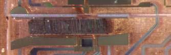
10 Micro Analysis Systems Members of our micro system family Optical spectrometer Paramagnetic oxygen sensor Gas chromatograph (GC) Temperature conductance Detector (TCD) Mass flow controller (MFC) commercialized Analyte concentrator Planar integrated micro mass spectrometer Flame Ionisation Detector t FID Vacuum pump with Pirani pressure sensor gas injector IR-gas detectors Periphery: valves, channels, membranes etc.
11 System approach Design of complete system with compatible subsystems system simulation with multi physics and mathematical tools development of process steps development of appropriate materials mask design fabrication with standard MEMS technologies development of appropriate electronics development of adjusted software characterization of subsystems and systems
12 Family Identity: anodically bonded glas - silicon - glass sandwich Technologies: Photolithography Thin film deposition (CVD, PVD) Advanced d Silicon Etch (ASE, Bosch) process Wet chemical and plasma etching


13 Fabrication in MEMS-Technology

14 Optical spectrometer nm 450 nm 350 nm 550 nm 500 nm 600 nm 650 nm 350 nm 1E-3 1E-4 1E-5 1E µm
15 SiO2-SiON-waveguides on silicon SiO 2 -SiON-SiO < n < 2.0 Process development: LPCVD process: SiH 2 Cl 2 -O 2 - NH 3 T = 930 C PECVD process: Si-wafer thermal oxidation LPCVD-SiO 2 SiON deposition SiO 2 deposition SiH 4 - O 2 - N 2 T = 350 C photolithography plasma etching p g Optical loss: < db/cm 1986 ridge waveguide
16 eff ficiency 0,6 05 0,5 0,4 0,3 0,2 0, wavelength / nm Spectral grating efficiency inten nsity & wavelength / nm Spectrum of a high pressure Hg-vapour bulb 16


17 Paramagnetic oxygen sensor


18 µ Gas Chromatograph GC-column integrated TCDs injector 10 C 1 8 [mv] TC CD bridge signal C 2 C 3 GC2001 SNG C 4 C 5 Mass flow sensor Time [sec]


19

20 2 Column µ-gc 160 mm 100mm
 reduced energy consumption small")

21 Micro mass spectrometer (PIMMS) small dimensions reduced vacuum requirements (1Pa) reduced energy consumption small analyte volume (pl) fast analysis a s (< 1s) mobile system low cost mass production field and in-line spectroscopy available
22 small dimensions Objectives high frequencies low capacitive loading (low power) low media consumption (gas, electrical power, analyte) chemically stable materials combination of electrically conductive and isolating materials established process technology reproducible batch fabrication on wafer scale use of standard electronics (voltages, currents, frequencies)


23 PIMMS Planar-Integrated Micro Mass Spectrometer Dimensions 7x10mm²
24 Realization Batch process for 100 devices on a 4 wafer Pressure in plasma and p ionization chamber installed via capillaries dimensions


25 Electron Source Dark-space reduction by variation of area ratio of electrodes previous new Electron extraction increased 40 from 2.5µA to ~37µA 30 µwave power ~200mW 20 Current [μa A] Chamber Pressure [Pa]


26 Synchronous Ion Shield Mass Separator path path-time-field-diagram electrical field orthogonal to ion flight path = field free = strong field only ions in field free region pass Ion cu urrent time mass


27 Redesigns Signal Generator for SIS four signals rise time < 1ns frequency range DC-50 MHz resolution < 0.1 Hz pulse height 5V linear scan of frequency or mass standard ICs used


28 Ion current amplifier High input impedance current to voltage converter Rise time < 3ms low noise < 0,2pA Directly adjacing PIMMS


29 Measurement set-up


30 Electronic boards µcontroller Current measurement I/O-interface spark ignition high voltage ± 230V voltage supply power connect Expected to be reduced to 3 to 5 ASICs


31 Software manual control of system components: HV-, RF-, DC-sources, SIS generator, etc. display of operating parameters and measurand automated booting of optimum operating parameters storage and booting of operating parameters recording, display, storage, and booting of spectra control of periphery: p pumps, p flow controllers, etc.


32 Software data recording linear in frequeny linear in mass display of spectra vs frequency vs mass Coice of resolution and measuring cycle time data storage individual multiple storage of comments with respect to indiviudal measurements Data format for storage: XML (EXtensible Markup Language)
33 Measurements
34 Micro Channel Plate Integration of a Micro Channel Plate (MCP) amplification >1.000 supply voltage <1,2 kv Pore- diameter 10µm aspect ratio 1:40 (Pore length 400µm)


35 Hybrid Integration of Micro Channel Plate
36 results Time for measurement: 4s Mass resolution: 32 (half peak width) air: N 2 28u 78% O 2 32u 21% Ar 40u 0,9% CO 2 44u 0,04% Xenon as plasma gas: Xe 131u Sensitivity ~ 100 ppm
 2 d f d = 800µmµ d = 1600µm")
37 results Variation of SIS-signal 2eU m = ( ) 2 d f d = 800µmµ d = 1600µm
38 results spectrum of Helium: width of finger electrodes increase by factor 2 Mass range shifted by factor 4 i.e. from 12u to 1200u to 3u to 300u
39 hydrogen
40 Methane resolution (FWHM) : 32 range: 0,5 m/z 50 m/z noise after averaging: 0,02 pa


41 Summary PIMMS MEMS approach allows for: cost efficient mass production portability new fields of application reduced requirements for base pressure may allows to use micro pumps resolution in the range of 3 bis >200 amu demonstrated sensitivity better than per mille mass resolution > 35 time response of electronics τ = 3 ms spectrum from 3 to 150 amu recorded in 4s
42 FID Quantitative measurement of organic compounds Measurement principle: Hydrogen flame ionization Electrical field (200 to 600V) generates ion current Applications: Gas Chromatography (GC) Total Hydrocarbon Analysis (THA) Disadvantages: Hydrogen High synthetic air consumption High voltage Ignition Anode Cathode Flame Air ~ 300 sccm H 2 ~ 30 sccm 2 Sample gas

43 cc-µfid Design Advantages: Encapsulated flame pure oxygen instead of synthetic air Thermally isolating glass substrates Stable counter-current flame with stagnation point: Minimal heat loss due to forced convection Long residence time of the sample in the flame Ion current saturation at low voltages
44 cc-µfid Design H2 + sample inlet H2 + sample nozzle Ignition Bond pad Si electrode Temp. sensor O2 inlet O2 nozzle Cr Guard SiO2 isolation Pt measurementt electrode l t d


45 cc-µfid Ignition
46 cc-µfid Temperature sensing Temperature at H 2 = O 2 = 7.5 ml/min measures 210 C
47 cc-µfid I vs. U H 2 = O 2 = ml/min, CH 4 in N 2.0ml/min Saturation below 10V for small concentrations


48 cc-µfid Performance ml/min H 2, 1%CH 4 in 2.0ml/min N 2 O 2 brightness, sensitivity


49 cc-µfid Performance ml/min H 2, 1%CH 4 in 2.0ml/min N 2 O 2 brightness, sensitivity
 O 2 (ml/min) Sensitivity (mc/gc) P-P Noise (pa) MDL (gc/s) Planar cc-µfid 75 7.5 11.25 11.9 04 0.")
50 cc-µfid Performance H 2 = 7.5ml/min, 1%CH 4 in N 2 = 2.0ml/min H 2 =O 2 = 7.5ml/min, N 2 = 2.0ml/min FID type H 2 (ml/min) O 2 (ml/min) Sensitivity (mc/gc) P-P Noise (pa) MDL (gc/s) Planar cc-µfid cc-fid FID conv AIR


51 Micro pump concept objectives: pump power > 1 ml/min starting from normal pressure base pressure: < 1 Pa electrically driven no additional media necessary energy and volume requirements similar to MEMS vapour jet pump
52 Micro vapour jet pump liquid vapourized by heater (platinum) nozzles generate vapour jet vapour condenses fluid assembles in reservoir porous membrane delivers liquid to heater ( sponge -principle) [channels connect reservoir to membrane]


53 Micro vapour jet pump liquid vapourized by heater (platinum) nozzles generate vapour jet vapour condenses fluid assembles in reservoir porous membrane delivers liquid to heater ( sponge -principle) [channels connect reservoir to membrane] Pirani pressure sensor
54 MEMS Vapor-Jet Vacuum Pump Ultimate Pre essure / mba ar μm 90 μm 125 μmμ Supply Pressure / bar p min = 500 mbar put / ml/min Through (working fluid: water vapor) Supply pressure e / bar


55 Funded by


56 Thank You for Thank You for your attention
Enable Highly-Stable Plasma Operations at High Pressures with the Right RPS Solution
 Enable Highly-Stable Plasma Operations at High Pressures with the Right RPS Solution Created by Advanced Energy Industries, Inc., Fort Collins, CO Abstract Conventional applications for remote plasma sources
Hermetic Packaging Solutions using Borosilicate Glass Thin Films. Lithoglas Hermetic Packaging Solutions using Borosilicate Glass Thin Films
 Hermetic Packaging Solutions using Borosilicate Glass Thin Films 1 Company Profile Company founded in 2006 ISO 9001:2008 qualified since 2011 Headquarters and Production in Dresden, Germany Production
Real time plasma etch control by means of physical plasma parameters with HERCULES
 Real time plasma etch control by means of physical plasma parameters with HERCULES A. Steinbach 1) S. Bernhard 1) M. Sussiek 4) S. Wurm 2) Ch. Koelbl 3) D. Knobloch 1) Siemens, Dresden Siemens at International
CMP for More Than Moore
 2009 Levitronix Conference on CMP Gerfried Zwicker Fraunhofer Institute for Silicon Technology ISIT Itzehoe, Germany gerfried.zwicker@isit.fraunhofer.de Contents Moore s Law and More Than Moore Comparison:
Major Fabrication Steps in MOS Process Flow
 Major Fabrication Steps in MOS Process Flow UV light Mask oxygen Silicon dioxide photoresist exposed photoresist oxide Silicon substrate Oxidation (Field oxide) Photoresist Coating Mask-Wafer Alignment
Nanofluidic Diodes based on Nanotube Heterojunctions
 Supporting Information Nanofluidic Diodes based on Nanotube Heterojunctions Ruoxue Yan, Wenjie Liang, Rong Fan, Peidong Yang 1 Department of Chemistry, University of California, Berkeley, CA 94720, USA
Industrialization of Micro-Electro-Mechanical Systems. Werner Weber Infineon Technologies
 Industrialization of Micro-Electro-Mechanical Systems Werner Weber Infineon Technologies Semiconductor-based MEMS market MEMS Market 2004 (total 22.7 BUS$) Others mostly Digital Light Projection IR Sensors
Performance characteristics of a new wide range, fast settling electrometer design for a residual gas analysis mass spectrometer
 Performance characteristics of a new wide range, fast settling electrometer design for a residual gas analysis mass spectrometer MKS Spectra Products, January 2010 Design considerations for RGA components
Sensors & Transducers Published by IFSA Publishing, S. L., 2016
 Sensors & Transducers Published by IFSA Publishing, S. L., 2016 http://www.sensorsportal.com Development of a Novel High Reliable Si-Based Trace Humidity Sensor Array for Aerospace and Process Industry
BioInstrumentation Laboratory
 BioInstrumentation Laboratory Ian Hunter Vienna, May 22 2013 BioInstrumentation Lab, Mechanical Engineering, MIT - Robotic endoscopes - Needle-free drug delivery devices - Eye micro-surgery robots - High
N-Methyl-1-(6-methylpyridin-2-yl)propan-2-amine
propan-2-amine") H C N CH HN CH. GENERAL INFORMATION IUPAC Name: CAS#: Not Available Synonyms: Source: Appearance: Not Available DEA Reference Material Collection Pale yellow powder UV max (nm): Not Determined. CHEMICAL
H C N CH HN CH. GENERAL INFORMATION IUPAC Name: CAS#: Not Available Synonyms: Source: Appearance: Not Available DEA Reference Material Collection Pale yellow powder UV max (nm): Not Determined. CHEMICAL
Characterization of Common Electron Multipliers in Harsh Environments
 ELECTRO-OPTICS Characterization of Common Electron Multipliers in Harsh Environments The Pittsburgh Conference 2005 Poster Paper 1340-20 Bruce Laprade and Raymond Cochran BURLE Electro-Optics INC Introduction
PROFILE CONTROL OF A BOROSILICATE-GLASS GROOVE FORMED BY DEEP REACTIVE ION ETCHING. Teruhisa Akashi and Yasuhiro Yoshimura
 Stresa, Italy, 25-27 April 2007 PROFILE CONTROL OF A BOROSILICATE-GLASS GROOVE FORMED BY DEEP REACTIVE ION ETCHING Teruhisa Akashi and Yasuhiro Yoshimura Mechanical Engineering Research Laboratory (MERL),
Production of HPDs for the LHCb RICH Detectors
 Production of HPDs for the LHCb RICH Detectors LHCb RICH Detectors Hybrid Photon Detector Production Photo Detector Test Facilities Test Results Conclusions IEEE Nuclear Science Symposium Wyndham, 24 th
True Three-Dimensional Interconnections
 True Three-Dimensional Interconnections Satoshi Yamamoto, 1 Hiroyuki Wakioka, 1 Osamu Nukaga, 1 Takanao Suzuki, 2 and Tatsuo Suemasu 1 As one of the next-generation through-hole interconnection (THI) technologies,
D. Impedance probe fabrication and characterization
 D. Impedance probe fabrication and characterization This section summarizes the fabrication process of the MicroCard bioimpedance probes. The characterization process is also described and the main electrical
Chapter 3 Fabrication
 Chapter 3 Fabrication The total structure of MO pick-up contains four parts: 1. A sub-micro aperture underneath the SIL The sub-micro aperture is used to limit the final spot size from 300nm to 600nm for
Performance of Microchannel Plates Fabricated Using Atomic Layer Deposition
 Performance of Microchannel Plates Fabricated Using Atomic Layer Deposition Andrey Elagin on behalf of the LAPPD collaboration Introduction Performance (timing) Conclusions Large Area Picosecond Photo
POLYMER MICROSTRUCTURE WITH TILTED MICROPILLAR ARRAY AND METHOD OF FABRICATING THE SAME
 POLYMER MICROSTRUCTURE WITH TILTED MICROPILLAR ARRAY AND METHOD OF FABRICATING THE SAME Field of the Invention The present invention relates to a polymer microstructure. In particular, the present invention
HPR-30 Vacuum Process Gas Analyser A differentially pumped RGA system for vacuum process monitoring
 HPR-30 Vacuum Process Gas Analyser A differentially pumped RGA system for vacuum process monitoring HPR-30 vacuum process gas analyser To analyse processes with high dynamic range operating at pressures
Photonic Crystal Slot Waveguide Spectrometer for Detection of Methane
 Photonic Crystal Slot Waveguide Spectrometer for Detection of Methane Swapnajit Chakravarty 1, Wei-Cheng Lai 2, Xiaolong (Alan) Wang 1, Che-Yun Lin 2, Ray T. Chen 1,2 1 Omega Optics, 10306 Sausalito Drive,
HIQUAD. New high-end mass spectrometer! Fast, flexible and easy to operate.
 New high-end mass spectrometer! Fast, flexible and easy to operate. New high-end mass spectrometer! Fast, flexible and easy to operate. A modular solution for mass spectrometry With the new HiQuad mass
Fabrication and application of a wireless inductance-capacitance coupling microsensor with electroplated high permeability material NiFe
 Journal of Physics: Conference Series Fabrication and application of a wireless inductance-capacitance coupling microsensor with electroplated high permeability material NiFe To cite this article: Y H
Synthesis of Silicon. applications. Nanowires Team. Régis Rogel (Ass.Pr), Anne-Claire Salaün (Ass. Pr)
, Anne-Claire Salaün (Ass. Pr)") Synthesis of Silicon nanowires for sensor applications Anne-Claire Salaün Nanowires Team Laurent Pichon (Pr), Régis Rogel (Ass.Pr), Anne-Claire Salaün (Ass. Pr) Ph-D positions: Fouad Demami, Liang Ni,
Synthesis of Silicon nanowires for sensor applications Anne-Claire Salaün Nanowires Team Laurent Pichon (Pr), Régis Rogel (Ass.Pr), Anne-Claire Salaün (Ass. Pr) Ph-D positions: Fouad Demami, Liang Ni,
Integration and Optimization of Hardware and Software for a Differential Flow Modulated GCxGC
 Paper 170-2 Integration and Optimization of Hardware and Software for a Differential Flow Modulated GCxGC Roger Firor, James McCurry, Chunxiao Wang and Michael Feeney Agilent Technologies Wilmington, DE
Plasma Enhanced Chemical Vapor Deposition (PECVD) of Silicon Nitride (SiNx) Using Oxford Instruments System 100 PECVD
 of Silicon Nitride (SiNx) Using Oxford Instruments System 100 PECVD") University of Pennsylvania ScholarlyCommons Tool Data Browse by Type 2-28-2017 Plasma Enhanced Chemical Vapor Deposition (PECVD) of Silicon Nitride (SiNx) Using Oxford Instruments System 100 PECVD Meredith
University of Pennsylvania ScholarlyCommons Tool Data Browse by Type 2-28-2017 Plasma Enhanced Chemical Vapor Deposition (PECVD) of Silicon Nitride (SiNx) Using Oxford Instruments System 100 PECVD Meredith
Towards a fully integrated optical gyroscope using whispering gallery modes resonators
 Towards a fully integrated optical gyroscope using whispering gallery modes resonators T. Amrane 1, J.-B. Jager 2, T. Jager 1, V. Calvo 2, J.-M. Leger 1 1 CEA, LETI, Grenoble, France. 2 CEA, INAC-SP2M
DTU DANCHIP an open access micro/nanofabrication facility bridging academic research and small scale production
 DTU DANCHIP an open access micro/nanofabrication facility bridging academic research and small scale production DTU Danchip National Center for Micro- and Nanofabrication DTU Danchip DTU Danchip is Denmark
MEMS in ECE at CMU. Gary K. Fedder
 MEMS in ECE at CMU Gary K. Fedder Department of Electrical and Computer Engineering and The Robotics Institute Carnegie Mellon University Pittsburgh, PA 15213-3890 fedder@ece.cmu.edu http://www.ece.cmu.edu/~mems
High-performance MEMS square electrode quadrupole mass filters for chip-scale mass spectrometry
 High-performance MEMS square electrode quadrupole mass filters for chip-scale mass spectrometry The MIT Faculty has made this article openly available. Please share how this access benefits you. Your story
CMOS Digital Integrated Circuits Lec 2 Fabrication of MOSFETs
 CMOS Digital Integrated Circuits Lec 2 Fabrication of MOSFETs 1 CMOS Digital Integrated Circuits 3 rd Edition Categories of Materials Materials can be categorized into three main groups regarding their
CLUSTERLINE RAD VERSATILE DYNAMIC SPUTTER SYSTEM OPTOELECTRONICS, MEMS, PHOTONICS, WIRELESS
 CLUSTERLINE RAD VERSATILE DYNAMIC SPUTTER SYSTEM OPTOELECTRONICS, MEMS, PHOTONICS, WIRELESS CLUSTERLINE RAD Enabling your roadmap in thin film deposition The combination of Evatec s process know-how and
Advancing EDS Analysis in the SEM Quantitative XRF. International Microscopy Congress, September 5 th, Outline
 Advancing EDS Analysis in the SEM with in-situ Quantitative XRF Brian J. Cross (1) & Kenny C. Witherspoon (2) 1) CrossRoads Scientific, El Granada, CA 94018, USA 2) ixrf Systems, Inc., Houston, TX 77059,
Technology for the MEMS processing and testing environment. SUSS MicroTec AG Dr. Hans-Georg Kapitza
 Technology for the MEMS processing and testing environment SUSS MicroTec AG Dr. Hans-Georg Kapitza 1 SUSS MicroTec Industrial Group Founded 1949 as Karl Süss KG GmbH&Co. in Garching/ Munich San Jose Waterbury
Nano-structured superconducting single-photon detector
 Nano-structured superconducting single-photon detector G. Gol'tsman *a, A. Korneev a,v. Izbenko a, K. Smirnov a, P. Kouminov a, B. Voronov a, A. Verevkin b, J. Zhang b, A. Pearlman b, W. Slysz b, and R.
Project by: Dr. Jorge A. Diaz. Physics School, University of Costa Rica, National Center for High Technology (CENAT)
") Test of a Miniature Double-Focusing Mass Spectrometer for the Variable Specific Impulse Magnetoplasma Rocket (VASIMR) at the Advanced Space Propulsion Laboratory Project by: Dr. Jorge A. Diaz Physics School,
Test of a Miniature Double-Focusing Mass Spectrometer for the Variable Specific Impulse Magnetoplasma Rocket (VASIMR) at the Advanced Space Propulsion Laboratory Project by: Dr. Jorge A. Diaz Physics School,
Monolithically integrated InGaAs nanowires on 3D. structured silicon-on-insulator as a new platform for. full optical links
 Monolithically integrated InGaAs nanowires on 3D structured silicon-on-insulator as a new platform for full optical links Hyunseok Kim 1, Alan C. Farrell 1, Pradeep Senanayake 1, Wook-Jae Lee 1,* & Diana.
Thermal Conductivity Sensor for Leak or Pressure Detection MTCS2601. MTCS2601 silicon sensing die in SMD ceramic package
 Sensor Description Thermal Conductivity Sensor for Leak or Pressure Detection MTCS2601 MTCS2601 silicon sensing die in SMD ceramic package Thermal conductivity sensor for primary vacuum measurement Silicon
Micro-sensors - what happens when you make "classical" devices "small": MEMS devices and integrated bolometric IR detectors
 Micro-sensors - what happens when you make "classical" devices "small": MEMS devices and integrated bolometric IR detectors Dean P. Neikirk 1 MURI bio-ir sensors kick-off 6/16/98 Where are the targets
Superconducting Nanowire Single Photon Detector (SNSPD) integrated with optical circuits
 integrated with optical circuits") Superconducting Nanowire Single Photon Detector (SNSPD) integrated with optical circuits Marcello Graziosi, ESR 3 within PICQUE (Marie Curie ITN project) and PhD student marcello.graziosi@ifn.cnr.it Istituto
Superconducting Nanowire Single Photon Detector (SNSPD) integrated with optical circuits Marcello Graziosi, ESR 3 within PICQUE (Marie Curie ITN project) and PhD student marcello.graziosi@ifn.cnr.it Istituto
RF MEMS Simulation High Isolation CPW Shunt Switches
 RF MEMS Simulation High Isolation CPW Shunt Switches Authored by: Desmond Tan James Chow Ansoft Corporation Ansoft 2003 / Global Seminars: Delivering Performance Presentation #4 What s MEMS Micro-Electro-Mechanical
Photoresist erosion studied in an inductively coupled plasma reactor employing CHF 3
 Photoresist erosion studied in an inductively coupled plasma reactor employing CHF 3 M. F. Doemling, N. R. Rueger, and G. S. Oehrlein a) Department of Physics, University at Albany, State University of
PRISMAPLUS. The precise solution for mass spectrometry. Modular design. Powerful software. Wide range of applications.
 PRISMAPLUS The precise solution for mass spectrometry. Modular design. Powerful software. Wide range of applications. PRISMAPLUS The precise solution for mass spectrometry. The combination of high sensi
Des MEMS aux NEMS : évolution des technologies et des concepts aux travers des développements menés au LETI
 Des MEMS aux NEMS : évolution des technologies et des concepts aux travers des développements menés au LETI Ph. Robert 1 Content LETI at a glance From MEMS to NEMS: 30 years of technological evolution
XRF Instrumentation. Introduction to spectrometer
 XRF Instrumentation Introduction to spectrometer AMPTEK, INC., Bedford, MA 01730 Ph: +1 781 275 2242 Fax: +1 781 275 3470 sales@amptek.com 1 Instrument Excitation source Sample X-ray tube or radioisotope
PrismaPlus. The New Mass Spectrometer with the Added Plus! Modular Design. Powerful Software. Wide Range of Applications.
 PrismaPlus The New Mass Spectrometer with the Added Plus! Modular Design. Powerful Software. Wide Range of Applications. PrismaPlus The PrismaPlus innovation The optimum combination of high sensitivity,
2007-Novel structures of a MEMS-based pressure sensor
 C-(No.16 font) put by office 2007-Novel structures of a MEMS-based pressure sensor Chang-Sin Park(*1), Young-Soo Choi(*1), Dong-Weon Lee (*2) and Bo-Seon Kang(*2) (1*) Department of Mechanical Engineering,
Technology platforms of microsystems technology a key for results of basic research featuring fast economic efficiency
 Technologische Plattformen der Mikrosystemtechnik für die schnellere wirtschaftliche Wirksamkeit von Ergebnissen der Grundlagen- und angewandten Vorlaufforschung Technology platforms of microsystems technology
Fabrication Techniques of Optical ICs
 Fabrication Techniques of Optical ICs Processing Techniques Lift off Process Etching Process Patterning Techniques Photo Lithography Electron Beam Lithography Photo Resist ( Microposit MP1300) Electron
Supporting Information. Single-Nanowire Electrochemical Probe Detection for Internally Optimized Mechanism of
 Supporting Information Single-Nanowire Electrochemical Probe Detection for Internally Optimized Mechanism of Porous Graphene in Electrochemical Devices Ping Hu, Mengyu Yan, Xuanpeng Wang, Chunhua Han,*
Inkjet Filling of TSVs with Silver Nanoparticle Ink. Behnam Khorramdel, Matti Mäntysalo Tampere University of Technology ESTC 2014 Finland, Helsinki
 Inkjet Filling of TSVs with Silver Nanoparticle Ink Behnam Khorramdel, Matti Mäntysalo Tampere University of Technology ESTC 2014 Finland, Helsinki Outline Motivation for this study Inkjet in MEMS fabrication
Advances in microchannel plate detectors for UV/visible Astronomy
 Advances in microchannel plate detectors for UV/visible Astronomy Dr. O.H.W. Siegmund Space Sciences Laboratory, U.C. Berkeley Advances in:- Photocathodes (GaN, Diamond, GaAs) Microchannel plates (Silicon
Development of a MEMS-based Dielectric Mirror
 Development of a MEMS-based Dielectric Mirror A Report Submitted for the Henry Samueli School of Engineering Research Scholarship Program By ThanhTruc Nguyen June 2001 Faculty Supervisor Richard Nelson
IWORID J. Schmitz page 1. Wafer-level CMOS post-processing Jurriaan Schmitz
 IWORID J. Schmitz page 1 Wafer-level CMOS post-processing Jurriaan Schmitz IWORID J. Schmitz page 2 Outline Introduction on wafer-level post-proc. CMOS: a smart, but fragile substrate Post-processing steps
(12) Patent Application Publication (10) Pub. No.: US 2011/ A1
 Patent Application Publication (10) Pub. No.: US 2011/ A1") (19) United States US 20110165057A1 (12) Patent Application Publication (10) Pub. No.: US 2011/0165057 A1 Honda et al. (43) Pub. Date: (54) PLASMACVD DEVICE, DLC FILM, AND C23C I6/455 (2006.01) METHOD
(19) United States US 20110165057A1 (12) Patent Application Publication (10) Pub. No.: US 2011/0165057 A1 Honda et al. (43) Pub. Date: (54) PLASMACVD DEVICE, DLC FILM, AND C23C I6/455 (2006.01) METHOD
Capillary Flow Technology: GCxGC Flow Modulator GET A SECOND DIMENSION OF INFORMATION ON COMPLEX MIXTURES
 Capillary Flow Technology: GCxGC Flow Modulator GET A SECOND DIMENSION OF INFORMATION ON COMPLEX MIXTURES Maximize information while collecting and analyzing GC data Comprehensive two-dimensional GC, or
On-chip interrogation of a silicon-on-insulator microring resonator based ethanol vapor sensor with an arrayed waveguide grating (AWG) spectrometer
 spectrometer") On-chip interrogation of a silicon-on-insulator microring resonator based ethanol vapor sensor with an arrayed waveguide grating (AWG) spectrometer Nebiyu A. Yebo* a, Wim Bogaerts, Zeger Hens b,roel Baets
On-chip interrogation of a silicon-on-insulator microring resonator based ethanol vapor sensor with an arrayed waveguide grating (AWG) spectrometer Nebiyu A. Yebo* a, Wim Bogaerts, Zeger Hens b,roel Baets
New Pixel Circuits for Driving Organic Light Emitting Diodes Using Low-Temperature Polycrystalline Silicon Thin Film Transistors
 Chapter 4 New Pixel Circuits for Driving Organic Light Emitting Diodes Using Low-Temperature Polycrystalline Silicon Thin Film Transistors ---------------------------------------------------------------------------------------------------------------
Part 5-1: Lithography
 Part 5-1: Lithography Yao-Joe Yang 1 Pattern Transfer (Patterning) Types of lithography systems: Optical X-ray electron beam writer (non-traditional, no masks) Two-dimensional pattern transfer: limited
Characterization of Silicon-based Ultrasonic Nozzles
 Tamkang Journal of Science and Engineering, Vol. 7, No. 2, pp. 123 127 (24) 123 Characterization of licon-based Ultrasonic Nozzles Y. L. Song 1,2 *, S. C. Tsai 1,3, Y. F. Chou 4, W. J. Chen 1, T. K. Tseng
Plan Optik AG. Plan Optik AG PRODUCT CATALOGUE
 Plan Optik AG Plan Optik AG PRODUCT CATALOGUE 2 In order to service the high demand of wafers more quickly, Plan Optik provides off the shelf products in sizes from 2 up to 300mm diameter. Therefore Plan
Development of a Low Cost, Low Power, Miniature Sector Mass Spectrometer with IonCCD Detection
 Leidos Proprietary Development of a Low Cost, Low Power, Miniature Sector Mass Spectrometer with IonCCD Detection Leidos; MIT MTL; Northeastern University; OI Analytical Development Team Noah Christian,
The Extrel MAX Systems are UHV-compatible flange mounted Quadrupole Mass
 The Extrel MAX Systems are UHV-compatible flange mounted Quadrupole Mass Spectrometers. The Ionizer, Quadrupole Mass Filter, and Detector on a Mounting Flange are designed for inclusion in your experimental
End-of-line Standard Substrates For the Characterization of organic
 FRAUNHOFER INSTITUTe FoR Photonic Microsystems IPMS End-of-line Standard Substrates For the Characterization of organic semiconductor Materials Over the last few years, organic electronics have become
按一下以編輯母片標題樣式. Novel Small-Dimension Poly-Si TFTs with Improved Driving Current and Suppressed Short Channel Effects. Hsiao-Wen Zan and Chun-Yen Chang
 Novel Small-Dimension Poly-Si TFTs with Improved Driving Current and Suppressed Short Channel Effects Hsiao-Wen Zan and Chun-Yen Chang Institute of Electronics, National Chiao Tung University, TAIWAN 1
High Power RF MEMS Switch Technology
 High Power RF MEMS Switch Technology Invited Talk at 2005 SBMO/IEEE MTT-S International Conference on Microwave and Optoelectronics Conference Dr Jia-Sheng Hong Heriot-Watt University Edinburgh U.K. 1
Problems of the Processing Accuracy for Electro-erosion erosion and Electrochemical Machining Processes
 12th ESAFORM Conference on material forming Twente,, Nederland, 27 29 April 2009 MS13: Non-conventional processes Problems of the Processing Accuracy for Electro-erosion erosion and Electrochemical Processes
Microfabrication technologies for highly-laminated thick metallic cores and 3-D integrated windings
 Microfabrication technologies for highly-laminated thick metallic cores and 3-D integrated windings Florian Herrault Georgia Institute of Technology Atlanta, GA florian@gatech.edu http://mems.gatech.edu/msma
GaN Electrochemical Probes and MEMS on Silicon. Ulrich Heinle, Peter Benkart, Ingo Daumiller, Mike Kunze, Ertugrul Sönmez
 GaN Electrochemical Probes and MEMS on Silicon Ulrich Heinle, Peter Benkart, Ingo Daumiller, Mike Kunze, Ertugrul Sönmez Outline Introduction Electrochemical sensors GaN-on-Silicon MEMS High temperature
Lecture: Integration of silicon photonics with electronics. Prepared by Jean-Marc FEDELI CEA-LETI
 Lecture: Integration of silicon photonics with electronics Prepared by Jean-Marc FEDELI CEA-LETI Context The goal is to give optical functionalities to electronics integrated circuit (EIC) The objectives
Transistor was first invented by William.B.Shockley, Walter Brattain and John Bardeen of Bell Labratories. In 1961, first IC was introduced.
 Unit 1 Basic MOS Technology Transistor was first invented by William.B.Shockley, Walter Brattain and John Bardeen of Bell Labratories. In 1961, first IC was introduced. Levels of Integration:- i) SSI:-
Optimized Process Performance Using the Paramount /Navigator Power- Delivery/Match Solution
 Optimized Process Performance Using the Paramount /Navigator Power- Delivery/Match Solution Dan Carter, Advanced Energy Industries, Inc. Numerous challenges face designers and users of today s RF plasma
Introducing the Agilent 7000A Triple Quadrupole GC/MS
 Introducing the Agilent 7000A Triple Quadrupole GC/MS Paul Zavitsanos, Joe Weitzel, Monty Benefiel and Terry Sheehan May 2008 Page 1 What s a Triple Quad? Page 2 GC/MS Triple Quad (QQQ) Collision Gas (N2
Dispersive IR-Spectroscopy for harsh environment based on thermopile elements realized with TPL640 (thermopile line array)
") DOI.516/irs013/i3.4 Dispersive IR-Spectroscopy for harsh environment based on thermopile elements realized with TPL640 (thermopile line array) S. Biermann 1, P. Sachse 1, A. Magi 1, H. Klaubert 1, F. Hänschke
DOI.516/irs013/i3.4 Dispersive IR-Spectroscopy for harsh environment based on thermopile elements realized with TPL640 (thermopile line array) S. Biermann 1, P. Sachse 1, A. Magi 1, H. Klaubert 1, F. Hänschke
Performance Characterization Of A Simultaneous Positive and Negative Ion Detector For Mass Spectrometry Applications
 Performance Characterization Of A Simultaneous Positive and Negative Ion Detector For Mass Spectrometry Applications Bruce Laprade and Raymond Cochran Introduction Microchannel Plates (Figures 1) are parallel
Autoresonant Trap Mass Spectrometry
 8 th Harsh Environment Mass Spectrometry Wokshop Autoresonant Trap Mass Spectrometry (ART MS) Sept 21, 2011 Gerardo A. Brucker and G. Jeffery Rathbone Granville-Phillips Vacuum Instrumentation Brooks Automation,
Low-Cost Far-Infrared FPA based on High-Volume Pressure Sensor Process
 Low-Cost Far-Infrared FPA based on High-Volume Pressure Sensor Process Michael Krueger 1, Ingo Herrmann 1 Robert Bosch GmbH - Automotive Electronics, Tuebinger Str. 13, D-776 Reutlingen, Germany, michael.krueger@de.bosch.com
Characterization of SC CVD diamond detectors for heavy ions spectroscopy
 Characterization of SC CVD diamond detectors for heavy ions spectroscopy Characterization of SC CVD diamond detectors for heavy and ions MIPsspectroscopy timing and MIPs timing Michal Pomorski and GSI
KNOW TRAINING MORE WITH. PerkinElmer Training Catalogue 2013 Relevant, interactive, rich in content.
 PerkinElmer Training Catalogue 2013 Relevant, interactive, rich in content. KNOW MORE WITH TRAINING PERKINELMER MISSION For people. For the environment. For the shared goal of a healthier future. Improving
MEMS Sensors: From Automotive. CE Applications. MicroNanoTec Forum Innovations for Industry April 19 th Hannover, Germany
 MEMS Sensors: From Automotive to CE Applications MicroNanoTec Forum Innovations for Industry 2010 April 19 th Hannover, Germany Oliver Schatz, CTO 1 Engineering April 2010 GmbH 2009. All rights reserved,
835 Vacuum Quality Monitor (VQM TM ) 2012 Brooks Automation, Inc. Proprietary Information
 2012 Brooks Automation, Inc. Proprietary Information") 835 Vacuum Quality Monitor (VQM TM ) 2012 Brooks Automation, Inc. Proprietary Information The Revolutionary New Vacuum Quality Monitor World s Fastest, Accurate at low mass Single Gas Calibration Small
835 Vacuum Quality Monitor (VQM TM ) 2012 Brooks Automation, Inc. Proprietary Information The Revolutionary New Vacuum Quality Monitor World s Fastest, Accurate at low mass Single Gas Calibration Small
Wafer-level Vacuum Packaged X and Y axis Gyroscope Using the Extended SBM Process for Ubiquitous Robot applications
 Proceedings of the 17th World Congress The International Federation of Automatic Control Wafer-level Vacuum Packaged X and Y axis Gyroscope Using the Extended SBM Process for Ubiquitous Robot applications
The Department of Advanced Materials Engineering. Materials and Processes in Polymeric Microelectronics
 The Department of Advanced Materials Engineering Materials and Processes in Polymeric Microelectronics 1 Outline Materials and Processes in Polymeric Microelectronics Polymeric Microelectronics Process
Subminiature Photoionization VOC Sensor Boris Dolgov, Baseline-MOCON, Inc.
 Subminiature Photoionization VOC Sensor Boris Dolgov, Baseline-MOCON, Inc. Lyons, CO 80540, USA (303) 823-6661 boris.dolgov@baseline.cc 1 1. Objective Monitoring of Volatile Organic Compounds (VOCs) is
BMC s heritage deformable mirror technology that uses hysteresis free electrostatic
 Optical Modulator Technical Whitepaper MEMS Optical Modulator Technology Overview The BMC MEMS Optical Modulator, shown in Figure 1, was designed for use in free space optical communication systems. The
Diode Sensor Lab. Dr. Lynn Fuller
 ROCHESTER INSTITUTE OF TECHNOLOGY MICROELECTRONIC ENGINEERING Diode Sensor Lab Dr. Lynn Fuller Webpage: http://people.rit.edu/lffeee 82 Lomb Memorial Drive Rochester, NY 14623-5604 Tel (585) 475-2035 Fax
Unpolarized Cluster, Jet and Pellet Targets
 Unpolarized Cluster, Jet and Pellet Targets Intense Electron Beams Workshop Cornell University, June 17-19, 2015 Institut für Kernphysik Typical Requirements on Internal Targets Target material: H 2, D
The trigger system of the muon spectrometer of the ALICE experiment at the LHC
 The trigger system of the muon spectrometer of the ALICE experiment at the LHC Francesco Bossù for the ALICE collaboration University and INFN of Turin Siena, 09 June 2010 Outline 1 Introduction 2 Muon
A novel sputtering technique: Inductively Coupled Impulse Sputtering (ICIS)
") A novel sputtering technique: Inductively Coupled Impulse Sputtering (ICIS) LOCH, Daniel and EHIASARIAN, Arutiun Available
A novel sputtering technique: Inductively Coupled Impulse Sputtering (ICIS) LOCH, Daniel and EHIASARIAN, Arutiun Available
Applications Information
 Applications Information Window Materials % TRANSMISSION 100 90 80 70 60 50 40 30 20 10 UV Sapphire UV Quartz Pyrex & Glass 100 200 300 400 500 600 700 800 900 Wavelength (nm) Pyrex only In applications
Heterogeneous Technology Alliance. SOI MEMS Platform
 Heterogeneous Technology Alliance SOI MEMS Platform Added value of HTA SOI MEMS Platform to customers 23-Aug-11 Page 1 Attractive offering of HTA SOI MEMS Platform One-stop shop 1 Very extensive R&D resources,
Then the mass spectrometer should go to the field, in your hand, small as possible, light as possible, and operated with light battery.
 My name is Mo Yang from Korea Basic Science Institute. Everybody here knows that a mass spectrometer is the most powerful analytical tool in chemistry. However, the target samples you want to analyze are
Basic Components of Spectroscopic. Instrumentation
 Basic Components of Spectroscopic Ahmad Aqel Ifseisi Assistant Professor of Analytical Chemistry College of Science, Department of Chemistry King Saud University P.O. Box 2455 Riyadh 11451 Saudi Arabia
3D SOI elements for System-on-Chip applications
 Advanced Materials Research Online: 2011-07-04 ISSN: 1662-8985, Vol. 276, pp 137-144 doi:10.4028/www.scientific.net/amr.276.137 2011 Trans Tech Publications, Switzerland 3D SOI elements for System-on-Chip
State-of-the-art device fabrication techniques
 State-of-the-art device fabrication techniques! Standard Photo-lithography and e-beam lithography! Advanced lithography techniques used in semiconductor industry Deposition: Thermal evaporation, e-gun
Using Multi Way PCA (MPCA) for Advanced Monitoring and Diagnosis for Plasma Processing based on Optical Emission Spectroscopy
 for Advanced Monitoring and Diagnosis for Plasma Processing based on Optical Emission Spectroscopy") Page 1 Using Multi Way PCA (MPCA) for Advanced Monitoring and Diagnosis for Plasma Processing based on Optical Emission Spectroscopy Fraunhofer Infineon Technologies Dresden Infineon Technologies München
Page 1 Using Multi Way PCA (MPCA) for Advanced Monitoring and Diagnosis for Plasma Processing based on Optical Emission Spectroscopy Fraunhofer Infineon Technologies Dresden Infineon Technologies München
LC/MS/MS. Page Header. triple quadrupole mass spectrometer.
 LC/MS/MS VARIAN, INC. 320-MS Page Header triple quadrupole mass spectrometer www.varianinc.com VARIAN, INC. 320-MS Unsurpassed commitment to innovation Varian, Inc. is an innovator and leader in mass spectrometry
64 Channel Flip-Chip Mounted Selectively Oxidized GaAs VCSEL Array
 64 Channel Flip-Chip Mounted Selectively Oxidized GaAs VCSEL Array 69 64 Channel Flip-Chip Mounted Selectively Oxidized GaAs VCSEL Array Roland Jäger and Christian Jung We have designed and fabricated
Micro-manipulated Cryogenic & Vacuum Probe Systems
 Janis micro-manipulated probe stations are designed for non-destructive electrical testing using DC, RF, and fiber-optic probes. They are useful in a variety of fields including semiconductors, MEMS, superconductivity,
P-CUBE-Series High Sensitivity PIN Detector Modules
 High Sensitivity PIN Detector Modules Description The P-CUBE-series manufactured by LASER COMPONENTS has been designed for customers interested in experimenting with low noise silicon or InGaAs pin detectors.