Capacitive-Division Traveling-Wave Amplifier with 340 GHz Gain-Bandwidth Product
|
|
|
- Bennett Quinn
- 5 years ago
- Views:
Transcription
1 Hughes Presented at the 1995 IEEE MTT-S Symposium UCSB Capacitive-Division Traveling-Wave Amplifier with 340 GHz Gain-Bandwidth Product J. Pusl 1,2, B. Agarwal1, R. Pullela1, L. D. Nguyen 3, M. V. Le 3, M. J. W. Rodwell1, L. Larson 3, J. F. Jensen 3, R. Y. Yu1,4, M. G. Case1,3. 1 University of California, Santa Barbara 2 Now with Hughes Space & Communications Company 3 Hughes Research Laboratories 4 Now with Rockwell International Science Center Support: California MICRO / Hughes Research Laboratories ARPA Thunder and Lightning Program, AFOSR
2 Capacitive-Division Traveling-Wave Amplifier Traveling-wave (distributed) amplifier : standard broadband IC Capacitive division TWA: Ayasli, 1988 broadband power Capacitive division TWA: significantly larger gain-bandwidth product This work: InGaAs/InAlAs HEMT CDTWAs Result: 11 db gain, 96 GHz bandwidth Record 340 GHz gain-bandwidth product
3 Principles of Traveling-Wave Amplifiers Z 0 L /2 C d L C d Output L/2 Synthetic Drain Line Cascode FETs Input L/2 L L/2 Z 0 Synthetic Gate Line Broadband circuit. FET input / output capacitances absorbed into synthetic transmission lines. Gain-bandwidth limited by line losses resulting from FET resistive parasitics.
4 Synthetic Transmission Lines in TWAs line sections L line section inductance gate-source capacitance Characteristic impedance: C line section capacitance Z 0 = LC Cutoff frequency: f cutoff = 1 π LC
5 TWA Bandwidth Limited by Gate-Line Losses R i R i R i R i C gs input impedance of1st FET C gs FET input resistance Ri causes gate line attenuation transistors far from input not driven at high frequency this limits gain-bandwidth (Ayasli, 1982): C gs C gs Nth FET S f 2 21 high f τ 4πR i C gs...if drain line losses are small (cascode TWA)
6 Cascode Cell: Negligible Drain-Line Losses R i g m V g' s R ds C gs V g' s R i C gs V g' s g m V g' s R out R ds ( 1 + g m R ds ) much larger than R ds Cascode cell: very large output resistance drain line losses nearly eliminated model valid for frequencies significantly below fmax
7 Normal cascode TWAs are not optimal designs TWA Gain 15 Gains, db 10 5 Cascode MAG f/f max (frequency normalized to f max ) Gain-bandwidth is well below MAG of cascode cell because 50Ω load much smaller than cascode R out
8 Examine the Gain-Bandwidth Limit: S f 2 21 high f τ 4πR i C gs R i g m V g' s C gs V g' s R out Decreasing Ri increases gain-bandwidth... How can we decrease input resistance Ri?
9 Capacitive Division Reduces Input Resistance transistor sizes doubled V in 2C gs 2C gs added capacitor forms 2:1 voltage divider with 2W 2W 2C gs model V in 2 2C gs R i /2 2g m V g's V in 2C V g' s gs R out /2 same input capacitance, same net transconductance input & output resistances reduced 2:1 2:1 division shown; higher ratios possible
10 Capacitive Division Increases TWA Gain-Bandwidth V in transistor sizes C div increased K:1 KC gs capacitive voltage divider with ratio: C div C div + KC gs = 1 K input & output resistances reduced K:1 gate line losses reduced K:1 K:1 more stages can be used: more gain at any design bandwidth, gain improved K:1 S 21 2 f high f K τ 4πR i C gs
11 How Much Can Gain-Bandwidth Be Improved? Gain, db normal 2:1 division 3:1 division Cascode Cell MAG 0 simulation f/f max (frequency normalized to f max ) Large division ratios: drain losses now significant, limits gain-bandwidth gain-bandwidth approaches MAG limit optimal circuit big FETs, difficult layout
12 Implementation / Design Features Hughes Research Laboratories low noise HEMT InAlAs / InGaAs / InP HEMT 0.15 µm gate length ft = 160 GHz, fmax = 260 GHz Regular, periodic structure: element values from design equations not computer optimized all cells have same FET sizes, same line lengths Conservative design: 2:1 capacitive division ratio designed for positive gain slope vs. frequency design gain-bandwidth well below MAG limit common-gate damping resistors: stabilization
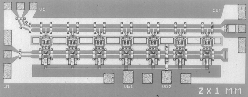
13 Die Photo
14 Measured Results: InP Capacitive-Division TWA S 21, db Wafer A: 10 db gain, 92 GHz bandwidth 5 0 Wafer B: 8 db gain, 98 GHz bandwidth Frequency, GHz Measured by UCSB 200 GHz on-wafer network analyzer Difference due to variation in Cgs & gm
15 Measured Results: InP Capacitive-Division TWA S 21, db 10 5 Wafer C: measured on 50 GHz HP8510 Wafer D: measured on W-Band HP Frequency, GHz 11 db gain, 96 GHz bandwidth 340 GHz gain-bandwidth product
16 DC-50 GHz Return Losses & Reverse Isolation 0-10 S 22 db S S Frequency, GHz S22 resonances due to test configuration (bias probe) Good input and output return losses
17 7-100 GHz Return Losses & Reverse Isolation 5 0 measured by UCSB 200 GHz wafer probe system S db S Frequency, GHz S12 better than 15 db below 100 GHz
18 Capacitive-Division TWA with 340 GHz Gain-Bandwidth Product Traveling-wave amplifier: broadband gain block Ayasli, 1988: capacitive division TWA Capacitive division can sizably improve gain-bandwidth product Results for InGaAs/InAlAs amplifier: 11dB gain, 96 GHz bandwidth record 340 GHz gain-bandwidth product This work: conservative design results below limits of device technology Designs with 150 & 200 GHz target bandwidths currently in fabrication.
BROAD-BAND amplifiers find applications as gain blocks
 IEEE TRANSACTIONS ON MICROWAVE THEORY AND TECHNIQUES, VOL. 46, NO. 12, DECEMBER 1998 2553 112-GHz, 157-GHz, and 180-GHz InP HEMT Traveling-Wave Amplifiers Bipul Agarwal, Adele E. Schmitz, J. J. Brown,
ISSCC 2004 / SESSION 26 / OPTICAL AND FAST I/O / 26.4
 ISSCC 2004 / SESSION 26 / OPTICAL AND FAST I/O / 26.4 26.4 40Gb/s CMOS Distributed Amplifier for Fiber-Optic Communication Systems H. Shigematsu 1, M. Sato 1, T. Hirose 1, F. Brewer 2, M. Rodwell 2 1 Fujitsu,
30% PAE W-band InP Power Amplifiers using Sub-quarter-wavelength Baluns for Series-connected Power-combining
 2013 IEEE Compound Semiconductor IC Symposium, October 13-15, Monterey, C 30% PAE W-band InP Power Amplifiers using Sub-quarter-wavelength Baluns for Series-connected Power-combining 1 H.C. Park, 1 S.
CHAPTER 4 ULTRA WIDE BAND LOW NOISE AMPLIFIER DESIGN
 93 CHAPTER 4 ULTRA WIDE BAND LOW NOISE AMPLIFIER DESIGN 4.1 INTRODUCTION Ultra Wide Band (UWB) system is capable of transmitting data over a wide spectrum of frequency bands with low power and high data
Design of a CMOS Distributed Power Amplifier with Gradual Changed Gain Cells
 Chinese Journal of Electronics Vol.27, No.6, Nov. 2018 Design of a CMOS Distributed Power Amplifier with Gradual Changed Gain Cells ZHANG Ying 1,2,LIZeyou 1,2, YANG Hua 1,2,GENGXiao 1,2 and ZHANG Yi 1,2
ETI , Good luck! Written Exam Integrated Radio Electronics. Lund University Dept. of Electroscience
 und University Dept. of Electroscience EI170 Written Exam Integrated adio Electronics 2010-03-10, 08.00-13.00 he exam consists of 5 problems which can give a maximum of 6 points each. he total maximum
6.776 High Speed Communication Circuits Lecture 7 High Freqeuncy, Broadband Amplifiers
 6.776 High Speed Communication Circuits Lecture 7 High Freqeuncy, Broadband Amplifiers Massachusetts Institute of Technology February 24, 2005 Copyright 2005 by Hae-Seung Lee and Michael H. Perrott High
A GHz MICROWAVE UP CONVERSION MIXERS USING THE CONCEPTS OF DISTRIBUTED AND DOUBLE BALANCED MIXING FOR OBTAINING LO AND RF (LSB) REJECTION
 REJECTION") A 2-40 GHz MICROWAVE UP CONVERSION MIXERS USING THE CONCEPTS OF DISTRIBUTED AND DOUBLE BALANCED MIXING FOR OBTAINING LO AND RF (LSB) REJECTION M. Mehdi, C. Rumelhard, J. L. Polleux, B. Lefebvre* ESYCOM
A 2-40 GHz MICROWAVE UP CONVERSION MIXERS USING THE CONCEPTS OF DISTRIBUTED AND DOUBLE BALANCED MIXING FOR OBTAINING LO AND RF (LSB) REJECTION M. Mehdi, C. Rumelhard, J. L. Polleux, B. Lefebvre* ESYCOM
Dual-band LNA Design for Wireless LAN Applications. 2.4 GHz LNA 5 GHz LNA Min Typ Max Min Typ Max
 Dual-band LNA Design for Wireless LAN Applications White Paper By: Zulfa Hasan-Abrar, Yut H. Chow Introduction Highly integrated, cost-effective RF circuitry is becoming more and more essential to the
4-Bit Ka Band SiGe BiCMOS Digital Step Attenuator
 Progress In Electromagnetics Research C, Vol. 74, 31 40, 2017 4-Bit Ka Band SiGe BiCMOS Digital Step Attenuator Muhammad Masood Sarfraz 1, 2, Yu Liu 1, 2, *, Farman Ullah 1, 2, Minghua Wang 1, 2, Zhiqiang
DESIGN OF 3 TO 5 GHz CMOS LOW NOISE AMPLIFIER FOR ULTRA-WIDEBAND (UWB) SYSTEM
 SYSTEM") Progress In Electromagnetics Research C, Vol. 9, 25 34, 2009 DESIGN OF 3 TO 5 GHz CMOS LOW NOISE AMPLIFIER FOR ULTRA-WIDEBAND (UWB) SYSTEM S.-K. Wong and F. Kung Faculty of Engineering Multimedia University
Progress In Electromagnetics Research C, Vol. 9, 25 34, 2009 DESIGN OF 3 TO 5 GHz CMOS LOW NOISE AMPLIFIER FOR ULTRA-WIDEBAND (UWB) SYSTEM S.-K. Wong and F. Kung Faculty of Engineering Multimedia University
TU3B-1. An 81 GHz, 470 mw, 1.1 mm 2 InP HBT Power Amplifier with 4:1 Series Power Combining using Sub-quarter-wavelength Baluns
 TU3B-1 Student Paper Finalist An 81 GHz, 470 mw, 1.1 mm 2 InP HBT Power Amplifier with 4:1 Series Power Combining using Sub-quarter-wavelength Baluns H. Park 1, S. Daneshgar 1, J. C. Rode 1, Z. Griffith
Simulations of High Linearity and High Efficiency of Class B Power Amplifiers in GaN HEMT Technology
 Simulations of High Linearity and High Efficiency of Class B Power Amplifiers in GaN HEMT Technology Vamsi Paidi, Shouxuan Xie, Robert Coffie, Umesh K Mishra, Stephen Long, M J W Rodwell Department of
6.976 High Speed Communication Circuits and Systems Lecture 5 High Speed, Broadband Amplifiers
 6.976 High Speed Communication Circuits and Systems Lecture 5 High Speed, Broadband Amplifiers Michael Perrott Massachusetts Institute of Technology Copyright 2003 by Michael H. Perrott Broadband Communication
6-18 GHz MMIC Drive and Power Amplifiers
 JOURNAL OF SEMICONDUCTOR TECHNOLOGY AND SCIENCE, VOL.2, NO. 2, JUNE, 02 125 6-18 GHz MMIC Drive and Power Amplifiers Hong-Teuk Kim, Moon-Suk Jeon, Ki-Woong Chung, and Youngwoo Kwon Abstract This paper
ECE 145A / 218 C, notes set xx: Class A power amplifiers
 ECE 145A / 218 C, notes set xx: Class A power amplifiers Mark Rodwell University of California, Santa Barbara rodwell@ece.ucsb.edu 805-893-3244, 805-893-3262 fax Class A power amplifier: what do we mean?
Design of a Low Noise Amplifier using 0.18µm CMOS technology
 The International Journal Of Engineering And Science (IJES) Volume 4 Issue 6 Pages PP.11-16 June - 2015 ISSN (e): 2319 1813 ISSN (p): 2319 1805 Design of a Low Noise Amplifier using 0.18µm CMOS technology
1-13GHz Wideband LNA utilizing a Transformer as a Compact Inter-stage Network in 65nm CMOS
 -3GHz Wideband LNA utilizing a Transformer as a Compact Inter-stage Network in 65nm CMOS Hyohyun Nam and Jung-Dong Park a Division of Electronics and Electrical Engineering, Dongguk University, Seoul E-mail
Highly linear common-gate mixer employing intrinsic second and third order distortion cancellation
 Highly linear common-gate mixer employing intrinsic second and third order distortion cancellation Mahdi Parvizi a), and Abdolreza Nabavi b) Microelectronics Laboratory, Tarbiat Modares University, Tehran
A CMOS GHz UWB LNA Employing Modified Derivative Superposition Method
 Circuits and Systems, 03, 4, 33-37 http://dx.doi.org/0.436/cs.03.43044 Published Online July 03 (http://www.scirp.org/journal/cs) A 3. - 0.6 GHz UWB LNA Employing Modified Derivative Superposition Method
A 2.4GHz Cascode CMOS Low Noise Amplifier
 A 2.4GHz Cascode CMOS Low Noise Amplifier Gustavo Campos Martins, Fernando Rangel de Sousa Federal University of Santa Catarina (UFSC) Integrated Circuits Laboratory (LCI) August 31, 2012 G. C. Martins,
Small Signal Modelling of InGaAs/InAlAs phemt for low noise applications
 Small Signal Modelling of InGaAs/InAlAs phemt for low noise applications N. Ahmad and M. Mohamad Isa School of Microelectronic Engineering, Universiti Malaysia Perlis, Pauh Putra Campus, 26 Arau, Perlis,
Ultra High-Speed InGaAs Nano-HEMTs
 Ultra High-Speed InGaAs Nano-HEMTs 2003. 10. 14 Kwang-Seok Seo School of Electrical Eng. and Computer Sci. Seoul National Univ., Korea Contents Introduction to InGaAsNano-HEMTs Nano Patterning Process
Design A Distributed Amplifier System Using -Filtering Structure
 Kareem : Design A Distributed Amplifier System Using -Filtering Structure Design A Distributed Amplifier System Using -Filtering Structure Azad Raheem Kareem University of Technology, Control and Systems
ECE 145A and 218A. Transmission-line properties, impedance-matching exercises
 ECE 145A and 218A. Transmission-line properties, impedance-matching exercises Problem #1 This is a circuit file to study a transmission line. The 2 resistors are included to allow easy disconnection of
Amplifiers Frequency Response Examples
 ECE 5/45 Analog IC Design We will use the following MOSFET parameters for hand-calculations and the µm CMOS models for corresponding simulations. Table : Long-channel MOSFET parameters. Parameter NMOS
CHAPTER - 3 PIN DIODE RF ATTENUATORS
 CHAPTER - 3 PIN DIODE RF ATTENUATORS 2 NOTES 3 PIN DIODE VARIABLE ATTENUATORS INTRODUCTION An Attenuator [1] is a network designed to introduce a known amount of loss when functioning between two resistive
Design of a Low Power 5GHz CMOS Radio Frequency Low Noise Amplifier Rakshith Venkatesh
 Design of a Low Power 5GHz CMOS Radio Frequency Low Noise Amplifier Rakshith Venkatesh Abstract A 5GHz low power consumption LNA has been designed here for the receiver front end using 90nm CMOS technology.
DISTRIBUTED amplification is a popular technique for
 IEEE TRANSACTIONS ON CIRCUITS AND SYSTEMS II: EXPRESS BRIEFS, VOL. 58, NO. 5, MAY 2011 259 Compact Transformer-Based Distributed Amplifier for UWB Systems Aliakbar Ghadiri, Student Member, IEEE, and Kambiz
Design and Simulation of Voltage-Mode and Current-Mode Class-D Power Amplifiers for 2.4 GHz Applications
 Design and Simulation of Voltage-Mode and Current-Mode Class-D Power Amplifiers for 2.4 GHz Applications Armindo António Barão da Silva Pontes Abstract This paper presents the design and simulations of
INTRODUCTION TO ELECTRONICS EHB 222E
 INTRODUCTION TO ELECTRONICS EHB 222E MOS Field Effect Transistors (MOSFETS II) MOSFETS 1/ INTRODUCTION TO ELECTRONICS 1 MOSFETS Amplifiers Cut off when v GS < V t v DS decreases starting point A, once
SP 22.3: A 12mW Wide Dynamic Range CMOS Front-End for a Portable GPS Receiver
 SP 22.3: A 12mW Wide Dynamic Range CMOS Front-End for a Portable GPS Receiver Arvin R. Shahani, Derek K. Shaeffer, Thomas H. Lee Stanford University, Stanford, CA At submicron channel lengths, CMOS is
Single-stage G-band HBT Amplifier with 6.3 db Gain at 175 GHz
 Single-stage G-band HBT Amplifier with 6.3 db Gain at 175 GHz M. Urteaga, D. Scott, T. Mathew, S. Krishnan, Y. Wei, M.J.W. Rodwell Department of Electrical and Computer Engineering, University of California,
LABORATORY #3 QUARTZ CRYSTAL OSCILLATOR DESIGN
 LABORATORY #3 QUARTZ CRYSTAL OSCILLATOR DESIGN OBJECTIVES 1. To design and DC bias the JFET transistor oscillator for a 9.545 MHz sinusoidal signal. 2. To simulate JFET transistor oscillator using MicroCap
Chapter 8: Field Effect Transistors
 Chapter 8: Field Effect Transistors Transistors are different from the basic electronic elements in that they have three terminals. Consequently, we need more parameters to describe their behavior than
Low Noise Amplifier Design
 THE UNIVERSITY OF TEXAS AT DALLAS DEPARTMENT OF ELECTRICAL ENGINEERING EERF 6330 RF Integrated Circuit Design (Spring 2016) Final Project Report on Low Noise Amplifier Design Submitted To: Dr. Kenneth
A GSM Band Low-Power LNA 1. LNA Schematic
 A GSM Band Low-Power LNA 1. LNA Schematic Fig1.1 Schematic of the Designed LNA 2. Design Summary Specification Required Simulation Results Peak S21 (Gain) > 10dB >11 db 3dB Bandwidth > 200MHz (
10W Ultra-Broadband Power Amplifier
 (TH1B-01 ) 10W Ultra-Broadband Power Amplifier Amin K. Ezzeddine and Ho. C. Huang AMCOM Communications, Inc 401 Professional Drive, Gaithersburg, MD 20879, USA Tel: 301-353-8400 Email: amin@amcomusa.com
Unit III FET and its Applications. 2 Marks Questions and Answers
 Unit III FET and its Applications 2 Marks Questions and Answers 1. Why do you call FET as field effect transistor? The name field effect is derived from the fact that the current is controlled by an electric
High Gain Low Noise Amplifier Design Using Active Feedback
 Chapter 6 High Gain Low Noise Amplifier Design Using Active Feedback In the previous two chapters, we have used passive feedback such as capacitor and inductor as feedback. This chapter deals with the
A 60GHz CMOS Power Amplifier Using Varactor Cross-Coupling Neutralization with Adaptive Bias
 A 6GHz CMOS Power Amplifier Using Varactor Cross-Coupling Neutralization with Adaptive Bias Ryo Minami,Kota Matsushita, Hiroki Asada, Kenichi Okada,and Akira Tokyo Institute of Technology, Japan Outline
Low-Noise Amplifiers
 007/Oct 4, 31 1 General Considerations Noise Figure Low-Noise Amplifiers Table 6.1 Typical LNA characteristics in heterodyne systems. NF IIP 3 db 10 dbm Gain 15 db Input and Output Impedance 50 Ω Input
ECE 255, MOSFET Amplifiers
 ECE 255, MOSFET Amplifiers 26 October 2017 In this lecture, the basic configurations of MOSFET amplifiers will be studied similar to that of BJT. Previously, it has been shown that with the transistor
Simulation and Design Analysis of Integrated Receiver System for Millimeter Wave Applications
 Simulation and Design Analysis of Integrated Receiver System for Millimeter Wave Applications Rekha 1, Rajesh Kumar 2, Dr. Raj Kumar 3 M.R.K.I.E.T., REWARI ABSTRACT This paper presents the simulation and
TECHNICAL REPORT: CVEL
 TECHNICAL REPORT: CVEL-13-041 Preliminary Investigation of the Current Path and Circuit Parameters Associated with the Characteristic Ringing in a MOSFET Power Inverter J. Hunter Hayes and Dr. Todd Hubing
Chapter 2 CMOS at Millimeter Wave Frequencies
 Chapter 2 CMOS at Millimeter Wave Frequencies In the past, mm-wave integrated circuits were always designed in high-performance RF technologies due to the limited performance of the standard CMOS transistors
Lecture 25 - Frequency Response of Amplifiers (III) Other Amplifier Stages. December 8, 2005
 Other Amplifier Stages. December 8, 2005") 6.012 Microelectronic Devices and Circuits Fall 2005 Lecture 251 Lecture 25 Frequency Response of Amplifiers (III) Other Amplifier Stages December 8, 2005 Contents: 1. Frequency response of commondrain
6.012 Microelectronic Devices and Circuits Fall 2005 Lecture 251 Lecture 25 Frequency Response of Amplifiers (III) Other Amplifier Stages December 8, 2005 Contents: 1. Frequency response of commondrain
Evaluating and Optimizing Tradeoffs in CMOS RFIC Upconversion Mixer Design. by Dr. Stephen Long University of California, Santa Barbara
 Evaluating and Optimizing Tradeoffs in CMOS RFIC Upconversion Mixer Design by Dr. Stephen Long University of California, Santa Barbara It is not easy to design an RFIC mixer. Different, sometimes conflicting,
InGaP HBT MMIC Development
 InGaP HBT MMIC Development Andy Dearn, Liam Devlin; Plextek Ltd, Wing Yau, Owen Wu; Global Communication Semiconductors, Inc. Abstract InGaP HBT is being increasingly adopted as the technology of choice
Background (What Do Line and Load Transients Tell Us about a Power Supply?)
") Maxim > Design Support > Technical Documents > Application Notes > Power-Supply Circuits > APP 3443 Keywords: line transient, load transient, time domain, frequency domain APPLICATION NOTE 3443 Line and
Maxim > Design Support > Technical Documents > Application Notes > Power-Supply Circuits > APP 3443 Keywords: line transient, load transient, time domain, frequency domain APPLICATION NOTE 3443 Line and
Indium Phosphide and Related Materials Selectively implanted subcollector DHBTs
 Indium Phosphide and Related Materials - 2006 Selectively implanted subcollector DHBTs Navin Parthasarathy, Z. Griffith, C. Kadow, U. Singisetti, and M.J.W. Rodwell Dept. of Electrical and Computer Engineering,
Chapter 8: Field Effect Transistors
 Chapter 8: Field Effect Transistors Transistors are different from the basic electronic elements in that they have three terminals. Consequently, we need more parameters to describe their behavior than
DISTRIBUTED amplification, which was originally invented
 IEEE TRANSACTIONS ON CIRCUITS AND SYSTEMS II: EXPRESS BRIEFS, VOL. 56, NO. 3, MARCH 2009 185 A New Loss Compensation Technique for CMOS Distributed Amplifiers Kambiz Moez, Member, IEEE, and Mohamed Elmasry,
Multimode 2.4 GHz Front-End with Tunable g m -C Filter. Group 4: Nick Collins Trevor Hunter Joe Parent EECS 522 Winter 2010
 Multimode 2.4 GHz Front-End with Tunable g m -C Filter Group 4: Nick Collins Trevor Hunter Joe Parent EECS 522 Winter 2010 Overview Introduction Complete System LNA Mixer Gm-C filter Conclusion Introduction
EE70 - Intro. Electronics
 EE70 - Intro. Electronics Course website: ~/classes/ee70/fall05 Today s class agenda (November 28, 2005) review Serial/parallel resonant circuits Diode Field Effect Transistor (FET) f 0 = Qs = Qs = 1 2π
LECTURE 6 BROAD-BAND AMPLIFIERS
 ECEN 54, Spring 18 Active Microwave Circuits Zoya Popovic, University of Colorado, Boulder LECTURE 6 BROAD-BAND AMPLIFIERS The challenge in designing a broadband microwave amplifier is the fact that the
MP 4.3 Monolithic CMOS Distributed Amplifier and Oscillator
 MP 4.3 Monolithic CMOS Distributed Amplifier and Oscillator Bendik Kleveland, Carlos H. Diaz 1 *, Dieter Vook 1, Liam Madden 2, Thomas H. Lee, S. Simon Wong Stanford University, Stanford, CA 1 Hewlett-Packard
UNIT I BIASING OF DISCRETE BJT AND MOSFET PART A
 UNIT I BIASING OF DISCRETE BJT AND MOSFET PART A 1. Why do we choose Q point at the center of the load line? 2. Name the two techniques used in the stability of the q point.explain. 3. Give the expression
High Power Wideband AlGaN/GaN HEMT Feedback. Amplifier Module with Drain and Feedback Loop. Inductances
 High Power Wideband AlGaN/GaN HEMT Feedback Amplifier Module with Drain and Feedback Loop Inductances Y. Chung, S. Cai, W. Lee, Y. Lin, C. P. Wen, Fellow, IEEE, K. L. Wang, Fellow, IEEE, and T. Itoh, Fellow,
AMMC KHz 40 GHz Traveling Wave Amplifier
 AMMC- 3 KHz GHz Traveling Wave Amplifier Data Sheet Chip Size: Chip Size Tolerance: Chip Thickness: Pad Dimensions: 3 x µm (9. x 1.3 mils) ± µm (±. mils) ± µm ( ±. mils) 8 x 8 µm (.9 ±. mils) Description
ETIN25 Analogue IC Design. Laboratory Manual Lab 2
 Department of Electrical and Information Technology LTH ETIN25 Analogue IC Design Laboratory Manual Lab 2 Jonas Lindstrand Martin Liliebladh Markus Törmänen September 2011 Laboratory 2: Design and Simulation
An Asymmetrical Bulk CMOS Switch for 2.4 GHz Application
 Progress In Electromagnetics Research Letters, Vol. 66, 99 104, 2017 An Asymmetrical Bulk CMOS Switch for 2.4 GHz Application Lang Chen 1, * and Ye-Bing Gan 1, 2 Abstract A novel asymmetrical single-pole
Design and Implementation of a 1-5 GHz UWB Low Noise Amplifier in 0.18 um CMOS
 Downloaded from vbn.aau.dk on: marts 20, 2019 Aalborg Universitet Design and Implementation of a 1-5 GHz UWB Low Noise Amplifier in 0.18 um CMOS Shen, Ming; Tong, Tian; Mikkelsen, Jan H.; Jensen, Ole Kiel;
Quadrature GPS Receiver Front-End in 0.13μm CMOS: The QLMV cell
 1 Quadrature GPS Receiver Front-End in 0.13μm CMOS: The QLMV cell Yee-Huan Ng, Po-Chia Lai, and Jia Ruan Abstract This paper presents a GPS receiver front end design that is based on the single-stage quadrature
A 1.1V 150GHz Amplifier with 8dB Gain and +6dBm Saturated Output Power in Standard Digital 65nm CMOS Using Dummy-Prefilled Microstrip Lines
 A 1.1V 150GHz Amplifier with 8dB Gain and +6dBm Saturated Output Power in Standard Digital 65nm CMOS Using Dummy-Prefilled Microstrip Lines M. Seo 1, B. Jagannathan 2, C. Carta 1, J. Pekarik 3, L. Chen
University of Pittsburgh
 University of Pittsburgh Experiment #4 Lab Report MOSFET Amplifiers and Current Mirrors Submission Date: 07/03/2018 Instructors: Dr. Ahmed Dallal Shangqian Gao Submitted By: Nick Haver & Alex Williams
Code: 9A Answer any FIVE questions All questions carry equal marks *****
 II B. Tech II Semester (R09) Regular & Supplementary Examinations, April/May 2012 ELECTRONIC CIRCUIT ANALYSIS (Common to EIE, E. Con. E & ECE) Time: 3 hours Max Marks: 70 Answer any FIVE questions All
Design technique of broadband CMOS LNA for DC 11 GHz SDR
 Design technique of broadband CMOS LNA for DC 11 GHz SDR Anh Tuan Phan a) and Ronan Farrell Institute of Microelectronics and Wireless Systems, National University of Ireland Maynooth, Maynooth,Co. Kildare,
Application Note 0006
 VGS Transient Tolerance of Transphorm GaN FETs Abstract This document provides a guideline for allowable transient voltages between gate and source pins. Table of Contents Abstract... 1 Introduction...
Varactor Loaded Transmission Lines for Linear Applications
 Varactor Loaded Transmission Lines for Linear Applications Amit S. Nagra ECE Dept. University of California Santa Barbara Acknowledgements Ph.D. Committee Professor Robert York Professor Nadir Dagli Professor
65-nm CMOS, W-band Receivers for Imaging Applications
 65-nm CMOS, W-band Receivers for Imaging Applications Keith Tang Mehdi Khanpour Patrice Garcia* Christophe Garnier* Sorin Voinigescu University of Toronto, *STMicroelectronics University of Toronto 27
Lecture 13. Biasing and Loading Single Stage FET Amplifiers. The Building Blocks of Analog Circuits - III
 Lecture 3 Biasing and Loading Single Stage FET Amplifiers The Building Blocks of Analog Circuits III In this lecture you will learn: Current biasing of circuits Current sources and sinks for CS, CG, and
6.776 High Speed Communication Circuits Lecture 6 MOS Transistors, Passive Components, Gain- Bandwidth Issue for Broadband Amplifiers
 6.776 High Speed Communication Circuits Lecture 6 MOS Transistors, Passive Components, Gain- Bandwidth Issue for Broadband Amplifiers Massachusetts Institute of Technology February 17, 2005 Copyright 2005
Performance Analysis of a Low Power Low Noise 4 13 GHz Ultra Wideband LNA
 Performance Analysis of a Low Power Low Noise 4 13 GHz Ultra Wideband LNA J.Manjula #1, Dr.S.Malarvizhi #2 # ECE Department, SRM University, Kattangulathur, Tamil Nadu, India-603203 1 jmanjulathiyagu@gmail.com
Low noise Amplifier, simulated and measured.
 Low noise Amplifier, simulated and measured. Introduction: As a study project a low noise amplifier shaper for capacitive detectors in AMS 0.6 µm technology is designed and realised. The goal was to design
DESIGN ANALYSIS AND COMPARATIVE STUDY OF RF RECEIVER FRONT-ENDS IN 0.18-µM CMOS
 International Journal of Electrical and Electronics Engineering Research Vol.1, Issue 1 (2011) 41-56 TJPRC Pvt. Ltd., DESIGN ANALYSIS AND COMPARATIVE STUDY OF RF RECEIVER FRONT-ENDS IN 0.18-µM CMOS M.
California Eastern Laboratories
 California Eastern Laboratories AN143 Design of Power Amplifier Using the UPG2118K APPLICATION NOTE I. Introduction Renesas' UPG2118K is a 3-stage 1.5W GaAs MMIC power amplifier that is usable from approximately
ITT Technical Institute. ET215 Devices 1. Unit 7 Chapter 4, Sections
 ITT Technical Institute ET215 Devices 1 Unit 7 Chapter 4, Sections 4.1 4.3 Chapter 4 Section 4.1 Structure of Field-Effect Transistors Recall that the BJT is a current-controlling device; the field-effect
Advanced Operational Amplifiers
 IsLab Analog Integrated Circuit Design OPA2-47 Advanced Operational Amplifiers כ Kyungpook National University IsLab Analog Integrated Circuit Design OPA2-1 Advanced Current Mirrors and Opamps Two-stage
Lecture 17: BJT/FET Mixers/Mixer Noise
 EECS 142 Lecture 17: BJT/FET Mixers/Mixer Noise Prof. Ali M. Niknejad University of California, Berkeley Copyright c 2005 by Ali M. Niknejad A. M. Niknejad University of California, Berkeley EECS 142 Lecture
BJT Circuits (MCQs of Moderate Complexity)
") BJT Circuits (MCQs of Moderate Complexity) 1. The current ib through base of a silicon npn transistor is 1+0.1 cos (1000πt) ma. At 300K, the rπ in the small signal model of the transistor is i b B C r
BJT Circuits (MCQs of Moderate Complexity) 1. The current ib through base of a silicon npn transistor is 1+0.1 cos (1000πt) ma. At 300K, the rπ in the small signal model of the transistor is i b B C r
Analysis and design of a V-band low-noise amplifier in 90 nm CMOS for 60 GHz applications
 LETTER IEICE Electronics Express, Vol.12, No.1, 1 10 Analysis and design of a V-band low-noise amplifier in 90 nm CMOS for 60 GHz applications Zhenxing Yu 1a), Jun Feng 1, Yu Guo 2, and Zhiqun Li 1 1 Institute
Design Methodology and Applications of SiGe BiCMOS Cascode Opamps with up to 37-GHz Unity Gain Bandwidth
 Design Methodology and Applications of SiGe BiCMOS Cascode Opamps with up to 37-GHz Unity Gain Bandwidth S.P. Voinigescu, R. Beerkens*, T.O. Dickson, and T. Chalvatzis University of Toronto *STMicroelectronics,
LINEARITY IMPROVEMENT OF CASCODE CMOS LNA USING A DIODE CONNECTED NMOS TRANSISTOR WITH A PARALLEL RC CIRCUIT
 Progress In Electromagnetics Research C, Vol. 17, 29 38, 2010 LINEARITY IMPROVEMENT OF CASCODE CMOS LNA USING A DIODE CONNECTED NMOS TRANSISTOR WITH A PARALLEL RC CIRCUIT C.-P. Chang, W.-C. Chien, C.-C.
An E-band Voltage Variable Attenuator Realised on a Low Cost 0.13 m PHEMT Process
 An E-band Voltage Variable Attenuator Realised on a Low Cost 0.13 m PHEMT Process Abstract Liam Devlin and Graham Pearson Plextek Ltd (liam.devlin@plextek.com) E-band spectrum at 71 to 76GHz and 81 to
2-6 GHz GaN HEMT Power Amplifier MMIC with Bridged-T All-Pass Filters and Output-Reactance- Compensation Shorted Stubs
 JOURNAL OF SEMICONDUCTOR TECHNOLOGY AND SCIENCE, VOL.16, NO.3, JUNE, 2016 ISSN(Print) 1598-1657 http://dx.doi.org/10.5573/jsts.2016.16.3.312 ISSN(Online) 2233-4866 2-6 GHz GaN HEMT Power Amplifier MMIC
The Design of E-band MMIC Amplifiers
 The Design of E-band MMIC Amplifiers Liam Devlin, Stuart Glynn, Graham Pearson, Andy Dearn * Plextek Ltd, London Road, Great Chesterford, Essex, CB10 1NY, UK; (lmd@plextek.co.uk) Abstract The worldwide
Electronics Prof. D. C. Dube Department of Physics Indian Institute of Technology, Delhi
 Electronics Prof. D. C. Dube Department of Physics Indian Institute of Technology, Delhi Module No # 05 FETS and MOSFETS Lecture No # 06 FET/MOSFET Amplifiers and their Analysis In the previous lecture
ISSCC 2004 / SESSION 26 / OPTICAL AND FAST I/O / 26.6
 ISSCC 2004 / SESSION 26 / OPTICAL AND FAST I/O / 26.6 26.6 40Gb/s Amplifier and ESD Protection Circuit in 0.18µm CMOS Technology Sherif Galal, Behzad Razavi University of California, Los Angeles, CA Optical
ECEN 474/704 Lab 5: Frequency Response of Inverting Amplifiers
 ECEN 474/704 Lab 5: Frequency Response of Inverting Amplifiers Objective Design, simulate and layout various inverting amplifiers. Introduction Inverting amplifiers are fundamental building blocks of electronic
2.Circuits Design 2.1 Proposed balun LNA topology
 3rd International Conference on Multimedia Technology(ICMT 013) Design of 500MHz Wideband RF Front-end Zhengqing Liu, Zhiqun Li + Institute of RF- & OE-ICs, Southeast University, Nanjing, 10096; School
20 40 GHz Amplifier. Technical Data HMMC-5040
 2 4 GHz Amplifier Technical Data HMMC-4 Features Large Bandwidth: 2-44 GHz Typical - 4 GHz Specified High : db Typical Saturated Output Power: dbm Typical Supply Bias: 4. volts @ 3 ma Description The HMMC-4
F7 Transistor Amplifiers
 Lars Ohlsson 2018-09-25 F7 Transistor Amplifiers Outline Transfer characteristics Small signal operation and models Basic configurations Common source (CS) CS/CE w/ source/ emitter degeneration resistance
ANALOG FUNDAMENTALS C. Topic 4 BASIC FET AMPLIFIER CONFIGURATIONS
 AV18-AFC ANALOG FUNDAMENTALS C Topic 4 BASIC FET AMPLIFIER CONFIGURATIONS 1 ANALOG FUNDAMENTALS C AV18-AFC Overview This topic identifies the basic FET amplifier configurations and their principles of
G-Band ( GHz) InP-Based HBT Amplifiers
 InP-Based HBT Amplifiers") IEEE JOURNAL OF SOLID-STATE CIRCUITS, VOL. 38, NO. 9, SEPTEMBER 2003 1451 G-Band (140 220-GHz) InP-Based HBT Amplifiers Miguel Urteaga, Dennis Scott, Sundararajan Krishnan, Yun Wei, Mattias Dahlström,
IEEE JOURNAL OF SOLID-STATE CIRCUITS, VOL. 38, NO. 9, SEPTEMBER 2003 1451 G-Band (140 220-GHz) InP-Based HBT Amplifiers Miguel Urteaga, Dennis Scott, Sundararajan Krishnan, Yun Wei, Mattias Dahlström,
Radio-Frequency Circuits Integration Using CMOS SOI 0.25µm Technology
 Radio-Frequency Circuits Integration Using CMOS SOI.5µm Technology Frederic Hameau and Olivier Rozeau CEA/LETI - 7, rue des Martyrs -F-3854 GRENOBLE FRANCE cedex 9 frederic.hameau@cea.fr olivier.rozeau@cea.fr
L/S-Band 0.18 µm CMOS 6-bit Digital Phase Shifter Design
 6th International Conference on Mechatronics, Computer and Education Informationization (MCEI 06) L/S-Band 0.8 µm CMOS 6-bit Digital Phase Shifter Design Xinyu Sheng, a and Zhangfa Liu, b School of Electronic
LAB 4 : FET AMPLIFIERS
 LEARNING OUTCOME: LAB 4 : FET AMPLIFIERS In this lab, students design and implement single-stage FET amplifiers and explore the frequency response of the real amplifiers. Breadboard and the Analog Discovery
ISSCC 2003 / SESSION 10 / HIGH SPEED BUILDING BLOCKS / PAPER 10.8
 ISSCC 2003 / SESSION 10 / HIGH SPEED BUILDING BLOCKS / PAPER 10.8 10.8 10Gb/s Limiting Amplifier and Laser/Modulator Driver in 0.18µm CMOS Technology Sherif Galal, Behzad Razavi Electrical Engineering
95GHz Receiver with Fundamental Frequency VCO and Static Frequency Divider in 65nm Digital CMOS
 95GHz Receiver with Fundamental Frequency VCO and Static Frequency Divider in 65nm Digital CMOS Ekaterina Laskin, Mehdi Khanpour, Ricardo Aroca, Keith W. Tang, Patrice Garcia 1, Sorin P. Voinigescu University