Direct Detectors for FIR/submm Light: Overview of Existing & Emerging Concepts
|
|
|
- Ginger Harrell
- 5 years ago
- Views:
Transcription
1 Direct Detectors for FIR/submm Light: Overview of Existing & Emerging Concepts Albrecht Poglitsch FIR Detectors 1
2 Outline Direct FIR/submm Detectors in an Astronomical Context Photon Detectors Basics Semiconductor Bulk Photoconductors Photodiodes BIB Detectors STJ SQPC Readout electronics / multiplexers Bolometric Detectors Basics Thermometers (semiconducting, superconducting) Absorber coupled bolometers Antenna coupled bolometers Filled arrays vs. single mode horns Bolometers without thermal noise? Readout / multiplexers FIR Detectors 2
3 FIR Detectors for Present/Future Observatories Observatories Ground based mm/submm telescopes SOFIA Future FIR space observatories (SAFIR, FIR Interferometers) Instruments Imaging broadband photometers/polarimeters Medium resolution, wideband and/or imaging spectrometers Boundary conditions for detectors Very large span in power/pixel between photometry with warm, ground based telescope and spectroscopy with cryogenic space telescope BLIP taken for granted Speed and stability requirements depend on application Large format arrays (observing efficiency) multiplexing One device unlikely to be optimum for all needs FIR Detectors 3


4 Limiting Sensitivities and Detector Needs Noise = 10 photons (at 200 µm) after ½ s integration FIR Detectors 4

5 Side Remark: Coherent vs. Direct Detection FIR Detectors 5
6 Photon Detector Basics Ideal direct detection of light: Convert each photon reaching the detector into an electrical signal (before energy gets thermalized) and count Noise determined by fundamental limit of photon statistics Today s approximation in FIR detectors: Convert a fraction of the photons (quantum efficiency) into charge carriers and integrate charge Detector may add extra noise Analog readout electronics adds noise / has limited dynamic range and resolution FIR Detectors 6
7 Semiconductor Bulk Photoconductor hν>e g E c hν>e i E c E d hν>e i D D + D D D A A A A A E c E a E v E v E v intrinsic n-type extrinsic p-type Photon absorption generates mobile charge carriers Intrinsic PC: electron hole pair Extrinsic PC: electron or hole (+ ionized donor/acceptor) External electric field causes drift of carriers Measured as photocurrent in contact Photoconductive gain strongly bias-dependent impact on readout Recombination after mean life time τ / drift length l Recombination is reverse process of generation same statistics Fundamental noise limit 2 x photon noise (g-r noise) FIR Detectors 7
8 FIR Photoconductor Characteristics Extrinsic photoconductors only practical devices so far demonstrated NEP of ~ W/ Hz at low background sufficiently low dark current at non-demanding T (1.8 K) low doping concentration essential low absorption arrays assembled from individual, ~mm 3 size Ge detectors, limiting maximum array size to ~10 3 pixels beyond 120 µm complex mechanical stress mechanism necessary, maximum wavelength ~205 µm performance degradation from cosmic rays problematic transient response at low background potential of bulk devices has probably been used up Intrinsic, e.g. Hg 1-x Cd x Te, photoconductors are difficult to control for the small bandgaps needed Superlattice materials, where layer thickness rather than alloy composition determines bandgap, may be promising FIR Detectors 8


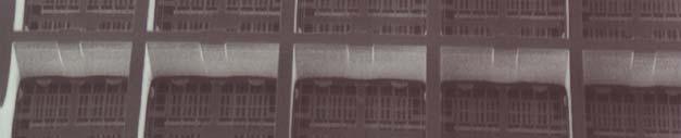
9 Ge:Ga Photoconductor Arrays MPIS 32 x 32 unstressed Ge:Ga array FIFI LS 16 x 25 stressed Ge:Ga array FIR Detectors 9
10 Photoconductor Transient Response and Memory Effects PC has two time constants (simplest model), light-level dependent τ g-r Cosmic rays can affect deeper states than FIR light and lead to responsivity change Calibration Curing schemes FIR Detectors 10
 is a composite semiconductor consisting of a large number of alternating well")
11 "Bandgap-Engineered" Semiconductors Bandgap of Hg1- x Cd x Te alloys vs. temperature for various Cd fractions x A superlattice (SL) is a composite semiconductor consisting of a large number of alternating well and barrier layers hence multiple quantum wells FIR Detectors 11
12 FIR Photodiodes? internal field (space charge in p-n transition) external field (reverse bias) Diode: space charge of p-n transition prevents transport of majority carriers Electron-hole pairs generated in or near transition by photon absorption separated by E-field bias independent, G=1 no g-r noise If semiconductor with sufficiently small bandgap (alloy or superlattice) becomes practical, photodiodes will be possible FIR Detectors 12
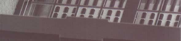
13 Blocked Impurity Band Detectors Advantages of BIB device: Small volume reduced cosmic ray susceptibility No g-r noise (diode-like) 2 gain in sensitivity over bulk device Monolithic, planar arrays large formats feasible Challenge: doping concentration profile (Ge:Ga BIB still no competitive QE) IR active layer 10 µm 4 µm metal contact implanted contact blocking layer Position (microns) FIR Detectors 13 Electric Field (V/cm) x cm -3 3 x cm -3 1 x cm -3 E y VB x U conduction band impurity conduction band
14 Read-out and Multiplexing Large-format detector arrays require cryogenic multiplexed readout electronics Fabrication of semiconductors devices for operation below K (carrier freeze-out) difficult Basic design depends on detector type Detectors with weak bias dependency (photodiodes) can use passive integration (e.g. into FET input capacitance) and source follower / switching multiplexer scheme Detectors with strong bias dependency (photoconductors) have to use active integrator (CTIA) circuit for each pixel + multiplexer Photoconductor readout is more complex than photodiode readout and more likely to introduce readout noise FIR Detectors 14
15 Passive Integration Multiplexer For bias-independent detectors, the passive integration scheme is simple affected by input voltage noise only after integration (read noise) Cryogenic MOS source follower standard Input capacitance used as integration capacitor Non-destructive, multiple read-out up the ramp V bias MUX Out Scheme used for NIR arrays with read noise ~ few electrons FIR Detectors 15
 affects integrated signal SBRC 190 FIR Detectors")
16 C f CTIA: Readout Scheme for PCs MUX Out In C AC -A C S/H -V bias CTIA architecture Capacitively fed-back highgain amplifier keeps input node at constant potential constant detector bias Photocurrent is integrated in feedback capacitor Amplifier input noise (both voltage & current noise density) affects integrated signal SBRC 190 FIR Detectors 16
17 Superconducting Tunnel Junction Single Quasiparticle Photon Counter (a) SQPC: Absorption of radiation, coupled in by an niobium antenna, breaks Cooper pairs in an aluminum strip and gives a current pulse through a tunnel junction connected to a RF-SET. (b) RF-SET: an input gate signal changes both SET output impedance and amount of rf carrier power reflected by a resonant LC-circuit. Reflected power is amplified by a HEMT for detection at room temperature. Multiple RF-SETs with different resonant frequencies can share the same HEMT. FIR Detectors 17
 Predicted NEP @ 300 GHz: 10-19 W/ Hz (limited by noise of bias resistor) Dynamic")
18 STJ SQPC (cont.) Predicted 300 GHz: W/ Hz (limited by noise of bias resistor) Dynamic range ~ R = on cryogenic space telescope FIR Detectors 18
19 NEP (W/ Hz) IR Group Science Retreat Ringberg, Nov 2002 Bolometer Basics Convert photon energy into heat that NEP at optimal bias vs optical power Red band //210 µm Si beam raises the temperature of the sensing element Some form of thermometer required to measure this temperature rise To maintain operating temperature, sensing element is connected through (weak) link to thermal photon bath thermal (phonon) noise, MOS requiring readout very low operating temperaturejohnson Current in (resistive) thermometer introduces (T-dependent) phonon load electrothermal feedback, affecting 10 speed/responsivity. Lower limit for -17 optical power (W) x 10 current by thermistor Johnson noise T=T 0 + T FIR Detectors 19 C P G R(T) T 0 U, I Responsivity: S= U/ P=IαR/G with α=1/r dr/dt Speed: τ=c/g Noise mechanisms: conventional bolometer photon background noise phonon noise: NEP= 4kT 2 G Johnson noise: NEP= 4kTR /S readout noise
20 New Variation on Theme: Integrating Bolometer Superconducting heat switch makes extremely weak link to bath. If brought to normal by magnetic field, conduction goes up by large factor (10 4 for Al at 100 mk) During integration very little phonon noise, then rapid reset. Correlated double sampling eliminates switching noise In combination with suitable thermometer, NEP < W/ Hz not precluded FIR Detectors 20
21 Bolometer Basics (cont.) Large variety of bolometer implementations comes from combination of: Two main technologies for thermometers semiconductive thermistor α<0, current biased superconductive oresistive: TES α>0, voltage biased; α very large o non-dissipative: kinetic inductance, magnetic penetration Two schemes of coupling to and dissipation of electromagnetic radiation Combined impedance matching and dissipation: absorber coupled bolometers this easily allows filled arrays Separate coupling and dissipation: antenna coupled bolometers antenna couples radiation into waveguide where it propagates to absorber (resistor) for dissipation, this allows beam shaping / straylight suppression + filtering FIR Detectors 21
22 Semiconductive thermistor Thermometers α<0, current biased measured quantity is voltage Ge (neutron transmutation doped) o Advantages: high α, very low 1/f knee (~0.02 Hz) odisadvantage:discrete bulk element, to be mounted/contacted on bolometer structure Si (ion implantation, diffusion, mesa,...) Ge (NTD) o Advantages: can be integrated in lithographic production process, allow very high impedances compatible with MOS noise o Disadvantages: not fully competitive in terms of 1/f onset and α FIR Detectors 22
23 Thermometers (cont.) Superconductor transition edge sensor (TES) Resistive, α > 0, voltage biased measured quantity is current, requiring special readout (in practice, SQUID) Extremely large α possible with proper design (homogeneous material + T, achieved by S/N sandwich) strong electrothermal feedback can decrease thermal τ by factor >100 or improve NEP phonon by factor >10 R TES Electrothermal feedback: TES can be thought of as a thermostat: best operating range (empirical) For constant U bias, R will adjust itself to keep the TES at T c by keeping P photon + U I = const I is directly proportional to P photon T C T FIR Detectors 23
24 Non-dissipative: kinetic inductance Thermometers (cont.) Surface impedance of superconductor is Figure (almost) entirely inductive (no DC resistance, but inertia of cooper pairs which have to be accelerated by AC field) Presence of quasiparticles (broken Cooper pairs) blocks some states for Cooper pairs and changes both parts of impedance Quasiparticle density grows exponentially with T (thermometer), but Cooper pairs can also be broken by photons with hν>2 photon detector FIR Detectors 24
25 Kinetic inductance Differential reactance and resistance follow quasiparticle density Quality factor Q=X/R grows exponentially with decreasing T T-measurement with microwave resonator: T-change leads to phase change in transmitted signal Different pixels can have resonators with different frequency (multiplexing) Thermometers (cont.) FIR Detectors 25
26 Thermometers (cont.) Non-dissipative: magnetic penetration Meissner-Ochsenfeld effect: no magnetic field in (bulk) superconductor Thin film: B(x) = B 0 exp(-x/λ), λ=f(t) Constant B-field, e.g. stored in superconducting drive coil on one side of thin film Pick-up coil on other side of film has to maintain magnetic flux by adjusting current accordingly Current in pick-up coil measured with SQUID Lossless, wireless thermometer! Superconducting thin film FIR Detectors 26 N S Magnetometer (SQUID) B 0 B(T)
 for better")
27 Absorber Bolometer: Resistive Film Thin film of e.g. Bi, matching free-space impedance, deposited on micromachined membrane, can be combined with λ/4 cavity (backreflector) for better efficiency FIR optical properties of 400 Ω/sq Bi/SiO bilayer on 1 µm SiN membrane FIR Detectors 27


28 Absorber Bolometer: Resistive Film (cont.) Filled array achieved by pop-up design which moves readout into 3rd dimension, linear modules densly stacked 1 µ PUDs Thick silicon frame mushroom bolometer: bolometer/readout sandwich Fabricated mainly by photolithography Load resistors mounted here Mushroom bolometer.065 K heat sink Works with either integrated Si thermistor or TES sensor Silicon Bridges 1.3 K heat sink Electrical pins Pop-up Device FIR Detectors 28
29 Absorber Bolometer: Resonant Grid Filled array Periodic absorber pattern + λ/4 cavity (backreflector) Use of compatible metal absorbers (superconductive, to reduce the heat capacity) Completely fabricated by photolithography Readout electronics indium-bump bonded to back of bolometer array to allow large size, butted arrays CMOS buffer/multiplexer (for semiconductive thermistors) Concept can be modified for TES Variation on theme: spiderweb bolometer same idea, but optimized for feed horn coupling FIR Detectors 29
30 Interconnection circuit CEA/LETI Design 0.3K >50 µm 400 µm Detection Layer thermometers silicon grid + absorber reflector Indium bumps indium bumps achieve, at the same time, the λ/4 cavity depth and electrical link between sensors and readout electronics FIR Detectors 30
31 CEA/LETI Design (cont.) Reference thermometer Pixel Pixel thermometer r Absorbing grid Silicon rod Thermistor impedance ~ Ω double SOI wafers 750 µm -2) MESA diffused thermometers. P:B FIR Detectors 31

32 FIR Detectors 32

33 Antenna Coupled Bolometers Single-moded horn antenna Heritage from coherent techniques Feedhorns where adjacent horn is used FWHM to couple beams one on the in the focal (Gaussian) plane mode into sky waveguide don t overlap Used in conjunction with e.g. spiderweb-absorber type bolometers in cavity for increased absorption efficiency and clean beam definition (no side lobes, no straylight from warmer parts of instrument) Good coupling requires ~2fλ diam. in focal plane which causes 2 FWHM beam spacing on sky Jiggling/special scanning for full beam sampling needed Beam FWHM λ/d Beam separation 2λ/D 16 pointings needed for fully-sampled image SPIRE PLW Array FIR Detectors 33
34 Filled Absorber vs. Horn Arrays Which gives better observing efficiency? It depends! Assumption: perfectly baffled system, only proper light from telescope aperture reaches focal plane (easier for horn!) Observation of point source with known position (+ no pointing errors): Gaussian horn receives one mode (signal + background) and couples ~80% of source power to detector. Filled array (fully sampling, with θaccordingly lower background) has to apply spatial filtering to signals from pixels around source position for best (S/N) power measurement. Gaussian horn wins by factor 1.2 in S/N Observation of point source with position/pointing accurate within region (λ/d) 2 : Gaussian horn needs jiggle (e.g. 7 positions around nominal). Filled array has to apply same spatial filtering to data, but with sliding center position. Filled array wins by factor 1.2 in S/N FIR Detectors 34
35 Filled Absorber vs. Horn Arrays (cont.) Mapping of extended area for point source extraction: (Further assumption: same focal plane size in both cases) Gaussian horn array, hexagonally packed, spaced by ~2 f# λ in focal plane effective focal plane ~0.3 For otherwise ~ comparable observing efficiency (see above), filled array gains factor of 3.4 in observing time! FIR Detectors 35
 Planar antenna structures Commonly used in coherent receivers Multiple slot antennae + microstripline seems favoured concept for bolometers Superconducting structures set upper limit in frequency")
36 Antenna Coupled Bolometers (cont.) Planar antenna structures Commonly used in coherent receivers Multiple slot antennae + microstripline seems favoured concept for bolometers Superconducting structures set upper limit in frequency Dual slot microstrip antenna, which is cut into a superconducting niobium ground plane, coupled to a TES. The electric field from the microstrip antenna is propagated along planar transmission lines. These microstrip lines consist of a niobium superconducting lead separated from the ground plane by 2000Ǻ of SiO dielectric. The electric fields from each antenna are passively added and terminated at a thin film Au resistor located on a thermally isolated silicon nitride island. On the same island, an Al/Ti/Au TES film responds to the temperature rise of the resistor. FIR Detectors 36
 Planar antenna structures Stripline allows integr")
37 Antenna Coupled Bolometers (cont.) Planar antenna structures Stripline allows integrated filter structures for e.g. multiband photometers, realized in one focal plane array FIR Detectors 37
38 Antenna Coupled Bolometers (cont.) Planar antenna structures Phased arrays (passively) of slot antennae allow beam shaping and potentially a good compromise between absorber and classical horn 4x3 phased array pixel (dual polarization) conceptual drawing Beam map and one row of 15x16 slot antenna array FIR Detectors 38
39 Readout and Multiplexing Current-biased bolometers need voltage readout Thermistors usually reasonably to very high impedance ontd Ge ~ 10MΩ, low enough for readout within ~10 cm. JFETs, heated to ~100K, have very low voltage noise and very low 1/f knee; used in most sensitive, really existing Low Frequency Noise Stability 10 bolometers. -5 No multiplexing at K or sub-k level possible, + hefty dissipation/ conduction from 100 K readout to cryogenic environment limits number of bolometers severely. FIR Detectors nv Hz -1/2 20 nv Hz -1/2 20 nv Hz -1/ Freq [Hz]
40 Readout and Multiplexing (cont.) Current-biased bolometers need voltage readout Thermistors usually reasonably to very high impedance o Si thermistors can be made with very high impedance (10 GΩ) for large voltage responsivity to become compatible with much higher voltage noise of cryogenic MOS FETs. This requires but also allows operation of readout within ~1 mm from sensor to keep RC low enough and prevent pickup. MOS technology allows complex circuits multiplexing. Also allows schemes for suppression of intrinsically too high 1/f knee. FIR Detectors 40
41 Differential Readout Scheme 300 mk VH RC RB VL VH VCH RC Rch RB VL 300 mk 300 mk VRL VDL VGL1 SEL2 SEL1 active pixels blind pixels SEL1 SEL2 VGL1 VDL VRL 300 mk SEL3 SEL3 Thermistor bridge for 2 K VDL_BU VDDeach pixel VGG1 VGL_BU1 Electronic chopping S1 between bridge and Buiffer Unit reference voltage to eliminate buffer 1/f noise Use of blind pixels to Buiffer reduce Unit influence of thermal drifts and EMI on signal lines S1 VGL_BU1 VGG1 VDD Achieved performance: 2 K VDL_BU NEP ~10-16 W/ 7 Hz bandwidth FIR Detectors 41
42 Readout and Multiplexing (cont.) Voltage-biased bolometers need current readout TES sensor has very low impedance; current needs to be measured at 0 voltage drop Presently, SQUID only realistic approach: TES current flows through s.c. coil, magnetic field measured with SQUID TES = I(T) B(T) I B V(T) V B SQUID SQUID is periodic device and requires somewhat complex control/readout electronics for operation FIR Detectors 42

43 High SQUID noise margin allows timedomain multiplexing Activation of individual pixel SQUIDS by bias through row select Amplification by serial SQUID array in each column Rigorous magnetic shielding mandatory! Readout and Multiplexing (cont.) FIR Detectors 43
Detection Beyond 100µm Photon detectors no longer work ("shallow", i.e. low excitation energy, impurities only go out to equivalent of
 Detection Beyond 100µm Photon detectors no longer work ("shallow", i.e. low excitation energy, impurities only go out to equivalent of 100µm) A few tricks let them stretch a little further (like stressing)
Based on lectures by Bernhard Brandl
 Astronomische Waarneemtechnieken (Astronomical Observing Techniques) Based on lectures by Bernhard Brandl Lecture 10: Detectors 2 1. CCD Operation 2. CCD Data Reduction 3. CMOS devices 4. IR Arrays 5.
Semiconductor Detector Systems
 Semiconductor Detector Systems Helmuth Spieler Physics Division, Lawrence Berkeley National Laboratory OXFORD UNIVERSITY PRESS ix CONTENTS 1 Detector systems overview 1 1.1 Sensor 2 1.2 Preamplifier 3
Micro-sensors - what happens when you make "classical" devices "small": MEMS devices and integrated bolometric IR detectors
 Micro-sensors - what happens when you make "classical" devices "small": MEMS devices and integrated bolometric IR detectors Dean P. Neikirk 1 MURI bio-ir sensors kick-off 6/16/98 Where are the targets
Background. Chapter Introduction to bolometers
 1 Chapter 1 Background Cryogenic detectors for photon detection have applications in astronomy, cosmology, particle physics, climate science, chemistry, security and more. In the infrared and submillimeter
Optical Fiber Communication Lecture 11 Detectors
 Optical Fiber Communication Lecture 11 Detectors Warriors of the Net Detector Technologies MSM (Metal Semiconductor Metal) PIN Layer Structure Semiinsulating GaAs Contact InGaAsP p 5x10 18 Absorption InGaAs
Quantum Sensors Programme at Cambridge
 Quantum Sensors Programme at Cambridge Stafford Withington Quantum Sensors Group, University Cambridge Physics of extreme measurement, tackling demanding problems in ultra-low-noise measurement for fundamental
Optical Receivers Theory and Operation
 Optical Receivers Theory and Operation Photo Detectors Optical receivers convert optical signal (light) to electrical signal (current/voltage) Hence referred O/E Converter Photodetector is the fundamental
Superconducting Transition-Edge Sensors and Superconducting Tunnel Junctions for Optical/UV Time-Energy Resolved Single-Photon Counters
 Superconducting Transition-Edge Sensors and Superconducting Tunnel Junctions for Optical/UV Time-Energy Resolved Single-Photon Counters NHST Meeting STScI - Baltimore 10 April 2003 TES & STJ Detector Summary
Detectors for Optical Communications
 Optical Communications: Circuits, Systems and Devices Chapter 3: Optical Devices for Optical Communications lecturer: Dr. Ali Fotowat Ahmady Sep 2012 Sharif University of Technology 1 Photo All detectors
VII. IR Arrays & Readout VIII.CCDs & Readout. This lecture course follows the textbook Detection of
 Detection of Light VII. IR Arrays & Readout VIII.CCDs & Readout This lecture course follows the textbook Detection of Light 4-3-2016 by George Rieke, Detection Cambridge of Light Bernhard Brandl University
Where detectors are used in science & technology
 Lecture 9 Outline Role of detectors Photomultiplier tubes (photoemission) Modulation transfer function Photoconductive detector physics Detector architecture Where detectors are used in science & technology
Fundamentals of CMOS Image Sensors
 CHAPTER 2 Fundamentals of CMOS Image Sensors Mixed-Signal IC Design for Image Sensor 2-1 Outline Photoelectric Effect Photodetectors CMOS Image Sensor(CIS) Array Architecture CIS Peripherals Design Considerations
Lecture 2. Part 2 (Semiconductor detectors =sensors + electronics) Segmented detectors with pn-junction. Strip/pixel detectors
 Segmented detectors with pn-junction. Strip/pixel detectors") Lecture 2 Part 1 (Electronics) Signal formation Readout electronics Noise Part 2 (Semiconductor detectors =sensors + electronics) Segmented detectors with pn-junction Strip/pixel detectors Drift detectors
Lecture 2 Part 1 (Electronics) Signal formation Readout electronics Noise Part 2 (Semiconductor detectors =sensors + electronics) Segmented detectors with pn-junction Strip/pixel detectors Drift detectors
Lecture 18: Photodetectors
 Lecture 18: Photodetectors Contents 1 Introduction 1 2 Photodetector principle 2 3 Photoconductor 4 4 Photodiodes 6 4.1 Heterojunction photodiode.................... 8 4.2 Metal-semiconductor photodiode................
First tests of prototype SCUBA-2 array
 First tests of prototype SCUBA-2 array Adam Woodcraft Astronomical Instrumentation Group School of Physics and Astronomy,Cardiff University http://woodcraft.lowtemp lowtemp.org/ Techniques and Instrumentation
SRM INSTITUTE OF SCIENCE AND TECHNOLOGY (DEEMED UNIVERSITY)
") SRM INSTITUTE OF SCIENCE AND TECHNOLOGY (DEEMED UNIVERSITY) QUESTION BANK I YEAR B.Tech (II Semester) ELECTRONIC DEVICES (COMMON FOR EC102, EE104, IC108, BM106) UNIT-I PART-A 1. What are intrinsic and
SRM INSTITUTE OF SCIENCE AND TECHNOLOGY (DEEMED UNIVERSITY) QUESTION BANK I YEAR B.Tech (II Semester) ELECTRONIC DEVICES (COMMON FOR EC102, EE104, IC108, BM106) UNIT-I PART-A 1. What are intrinsic and
Three Ways to Detect Light. We now establish terminology for photon detectors:
 Three Ways to Detect Light In photon detectors, the light interacts with the detector material to produce free charge carriers photon-by-photon. The resulting miniscule electrical currents are amplified
Magnetic and Electromagnetic Microsystems. 4. Example: magnetic read/write head
 Magnetic and Electromagnetic Microsystems 1. Magnetic Sensors 2. Magnetic Actuators 3. Electromagnetic Sensors 4. Example: magnetic read/write head (C) Andrei Sazonov 2005, 2006 1 Magnetic microsystems
OPTOELECTRONIC and PHOTOVOLTAIC DEVICES
 OPTOELECTRONIC and PHOTOVOLTAIC DEVICES Outline 1. Introduction to the (semiconductor) physics: energy bands, charge carriers, semiconductors, p-n junction, materials, etc. 2. Light emitting diodes Light
Antenna-coupled bolometer arrays for measurement of the Cosmic Microwave Background polarization
 Journal of Low Temperature Physics manuscript No. (will be inserted by the editor) M. J. Myers a K. Arnold a P. Ade b G. Engargiola c W. Holzapfel a A. T. Lee a X. Meng d R. O Brient a P. L. Richards a
14.2 Photodiodes 411
 14.2 Photodiodes 411 Maximum reverse voltage is specified for Ge and Si photodiodes and photoconductive cells. Exceeding this voltage can cause the breakdown and severe deterioration of the sensor s performance.
Superconducting Transition Edge Sensor Bolometer Arrays for Submillimeter Astronomy
 Superconducting Transition Edge Sensor Bolometer Arrays for Submillimeter Astronomy Dominic J. Benford, Christine A. Allen, Alexander S. Kutyrev, S. Harvey Moseley, Richard A. Shafer NASA - Goddard Space
Simulation of High Resistivity (CMOS) Pixels
 Pixels") Simulation of High Resistivity (CMOS) Pixels Stefan Lauxtermann, Kadri Vural Sensor Creations Inc. AIDA-2020 CMOS Simulation Workshop May 13 th 2016 OUTLINE 1. Definition of High Resistivity Pixel Also
Simulation of High Resistivity (CMOS) Pixels Stefan Lauxtermann, Kadri Vural Sensor Creations Inc. AIDA-2020 CMOS Simulation Workshop May 13 th 2016 OUTLINE 1. Definition of High Resistivity Pixel Also
Chap14. Photodiode Detectors
 Chap14. Photodiode Detectors Mohammad Ali Mansouri-Birjandi mansouri@ece.usb.ac.ir mamansouri@yahoo.com Faculty of Electrical and Computer Engineering University of Sistan and Baluchestan (USB) Design
Lecture 4 INTEGRATED PHOTONICS
 Lecture 4 INTEGRATED PHOTONICS What is photonics? Photonic applications use the photon in the same way that electronic applications use the electron. Devices that run on light have a number of advantages
A New Multiplexable Superconducting Detector
 A New Multiplexable Superconducting Detector Jonas Zmuidzinas California Institute of Technology Supported by: NASA Code R, A. Lidow Caltech Trustee, Caltech President s Fund, JPL DRDF Caltech Anastasios
Figure Responsivity (A/W) Figure E E-09.
 Figure E E-09.") OSI Optoelectronics, is a leading manufacturer of fiber optic components for communication systems. The products offer range for Silicon, GaAs and InGaAs to full turnkey solutions. Photodiodes are semiconductor
OSI Optoelectronics, is a leading manufacturer of fiber optic components for communication systems. The products offer range for Silicon, GaAs and InGaAs to full turnkey solutions. Photodiodes are semiconductor
Silicon sensors for radiant signals. D.Sc. Mikko A. Juntunen
 Silicon sensors for radiant signals D.Sc. Mikko A. Juntunen 2017 01 16 Today s outline Introduction Basic physical principles PN junction revisited Applications Light Ionizing radiation X-Ray sensors in
Coherent Receivers Principles Downconversion
 Coherent Receivers Principles Downconversion Heterodyne receivers mix signals of different frequency; if two such signals are added together, they beat against each other. The resulting signal contains
The superconducting microcalorimeters array for the X IFU instrument on board of Athena Luciano Gottardi
 The superconducting microcalorimeters array for the X IFU instrument on board of Athena Luciano Gottardi 13th Pisa meeting on advanced detectors Isola d'elba, Italy, May 24 30, 2015 Advance Telescope for
Photodiode: LECTURE-5
 LECTURE-5 Photodiode: Photodiode consists of an intrinsic semiconductor sandwiched between two heavily doped p-type and n-type semiconductors as shown in Fig. 3.2.2. Sufficient reverse voltage is applied
Fabrication of Feedhorn-Coupled Transition Edge Sensor Arrays for Measurement of the Cosmic Microwave Background Polarization
 Fabrication of Feedhorn-Coupled Transition Edge Sensor Arrays for Measurement of the Cosmic Microwave Background Polarization K.L Denis 1, A. Ali 2, J. Appel 2, C.L. Bennett 2, M.P.Chang 1,3, D.T.Chuss
LEDs, Photodetectors and Solar Cells
 LEDs, Photodetectors and Solar Cells Chapter 7 (Parker) ELEC 424 John Peeples Why the Interest in Photons? Answer: Momentum and Radiation High electrical current density destroys minute polysilicon and
Figure Figure E E-09. Dark Current (A) 1.
 1.") OSI Optoelectronics, is a leading manufacturer of fiber optic components for communication systems. The products offer range for Silicon, GaAs and InGaAs to full turnkey solutions. Photodiodes are semiconductor
OSI Optoelectronics, is a leading manufacturer of fiber optic components for communication systems. The products offer range for Silicon, GaAs and InGaAs to full turnkey solutions. Photodiodes are semiconductor
High-speed Ge photodetector monolithically integrated with large cross silicon-on-insulator waveguide
 [ APPLIED PHYSICS LETTERS ] High-speed Ge photodetector monolithically integrated with large cross silicon-on-insulator waveguide Dazeng Feng, Shirong Liao, Roshanak Shafiiha. etc Contents 1. Introduction
Lecture 19 Optical Characterization 1
 Lecture 19 Optical Characterization 1 1/60 Announcements Homework 5/6: Is online now. Due Wednesday May 30th at 10:00am. I will return it the following Wednesday (6 th June). Homework 6/6: Will be online
Two Level System Noise (TLS) and RF Readouts. Christopher McKenney. 4 th Microresonator Workshop 29 th July, 2011
 and RF Readouts. Christopher McKenney. 4 th Microresonator Workshop 29 th July, 2011") Two Level System Noise (TLS) and RF Readouts Christopher McKenney 4 th Microresonator Workshop 29 th July, 2011 Two Level System (TLS) and Superconducting Resonators Have well known effects in superconducting
Two Level System Noise (TLS) and RF Readouts Christopher McKenney 4 th Microresonator Workshop 29 th July, 2011 Two Level System (TLS) and Superconducting Resonators Have well known effects in superconducting
IV DETECTORS. Daguerrotype of the Moon, John W. Draper. March 26, 1840 New York
 IV DETECTORS Lit.: C.R.Kitchin: Astrophysical Techniques, 2009 C.D.Mckay: CCD s in Astronomy, Ann.Rev. A.&A. 24, 1986 G.H.Rieke: Infrared Detector Arrays for Astronomy, Ann.Rev. A&A 45, 2007 up to 1837:
UNIT VIII-SPECIAL PURPOSE ELECTRONIC DEVICES. 1. Explain tunnel Diode operation with the help of energy band diagrams.
 UNIT III-SPECIAL PURPOSE ELECTRONIC DEICES 1. Explain tunnel Diode operation with the help of energy band diagrams. TUNNEL DIODE: A tunnel diode or Esaki diode is a type of semiconductor diode which is
Advanced ACTPol Multichroic Horn-Coupled Polarimeter Array Fabrication on 150 mm Wafers
 Advanced ACTPol Multichroic Horn-Coupled Polarimeter Array Fabrication on 150 mm Wafers Shannon M. Duff NIST for the Advanced ACTPol Collaboration LTD16 22 July 2015 Grenoble, France Why Long-λ Detectors
OPTI510R: Photonics. Khanh Kieu College of Optical Sciences, University of Arizona Meinel building R.626
 OPTI510R: Photonics Khanh Kieu College of Optical Sciences, University of Arizona kkieu@optics.arizona.edu Meinel building R.626 Photodetectors Introduction Most important characteristics Photodetector
Submillimeter Instrumentation. Photo-detectors are no longer effective Submm astronomers use bolometers and heterodyne receivers.
 Submillimeter Instrumentation Photo-detectors are no longer effective Submm astronomers use bolometers and heterodyne receivers. Bolometers A bolometer consists of an absorber (efficiency ) attached to
Semiconductor Lasers Semiconductors were originally pumped by lasers or e-beams First diode types developed in 1962: Create a pn junction in
 Semiconductor Lasers Semiconductors were originally pumped by lasers or e-beams First diode types developed in 1962: Create a pn junction in semiconductor material Pumped now with high current density
Three Ways to Detect Light. Following: Lord Rosse image of M33 vs. Hubble image demonstrate how critical detector technology is.
 Three Ways to Detect Light In photon detectors, the light interacts with the detector material to produce free charge carriers photon-by-photon. The resulting miniscule electrical currents are amplified
Recent Development and Study of Silicon Solid State Photomultiplier (MRS Avalanche Photodetector)
") Recent Development and Study of Silicon Solid State Photomultiplier (MRS Avalanche Photodetector) Valeri Saveliev University of Obninsk, Russia Vienna Conference on Instrumentation Vienna, 20 February
Recent Development and Study of Silicon Solid State Photomultiplier (MRS Avalanche Photodetector) Valeri Saveliev University of Obninsk, Russia Vienna Conference on Instrumentation Vienna, 20 February
MICROWAVE ENGINEERING-II. Unit- I MICROWAVE MEASUREMENTS
 MICROWAVE ENGINEERING-II Unit- I MICROWAVE MEASUREMENTS 1. Explain microwave power measurement. 2. Why we can not use ordinary diode and transistor in microwave detection and microwave amplification? 3.
Single Sided and Double Sided Silicon MicroStrip Detector R&D
 Single Sided and Double Sided Silicon MicroStrip Detector R&D Tariq Aziz Tata Institute, Mumbai, India SuperBelle, KEK December 10-12, 2008 Indian Effort Mask Design at TIFR, Processing at BEL Single Sided
Moderne Teilchendetektoren - Theorie und Praxis 2. Dr. Bernhard Ketzer Technische Universität München SS 2013
 Moderne Teilchendetektoren - Theorie und Praxis 2 Dr. Bernhard Ketzer Technische Universität München SS 2013 7 Signal Processing and Acquisition 7.1 Signals 7.2 Amplifier 7.3 Electronic Noise 7.4 Analog-to-Digital
Aperture Efficiency of Integrated-Circuit Horn Antennas
 First International Symposium on Space Terahertz Technology Page 169 Aperture Efficiency of Integrated-Circuit Horn Antennas Yong Guo, Karen Lee, Philip Stimson Kent Potter, David Rutledge Division of
Penn Array Receiver Penn Array Receiver CDR Document 6: Detector Design Documents Table of Contents
 Penn Array Receiver Penn Array Receiver CDR Document 6: Detector Design Documents Version: 1 Date: 14 October 2003 Authors: Dominic Benford Table of Contents 1. Introduction...2 2. Detector Array Requirements...3
Lecture 8 Optical Sensing. ECE 5900/6900 Fundamentals of Sensor Design
 ECE 5900/6900: Fundamentals of Sensor Design Lecture 8 Optical Sensing 1 Optical Sensing Q: What are we measuring? A: Electromagnetic radiation labeled as Ultraviolet (UV), visible, or near,mid-, far-infrared
Ultrasonic. Advantages
 Ultrasonic Advantages Non-Contact: Nothing touches the target object Measures Distance: The distance to the target is measured, not just its presence Long and Short Range: Objects can be sensed from 2
Components of Optical Instruments
 Components of Optical Instruments General Design of Optical Instruments Sources of Radiation Wavelength Selectors (Filters, Monochromators, Interferometers) Sample Containers Radiation Transducers (Detectors)
Introduction: Planar Transmission Lines
 Chapter-1 Introduction: Planar Transmission Lines 1.1 Overview Microwave integrated circuit (MIC) techniques represent an extension of integrated circuit technology to microwave frequencies. Since four
Components of Optical Instruments 1
 Components of Optical Instruments 1 Optical phenomena used for spectroscopic methods: (1) absorption (2) fluorescence (3) phosphorescence (4) scattering (5) emission (6) chemiluminescence Spectroscopic
The SPICA-SAFARI TES Bolometer Readout: Developments Towards a Flight System
 J Low Temp Phys (2012) 167:561 567 DOI 10.1007/s10909-012-0521-y The SPICA-SAFARI TES Bolometer Readout: Developments Towards a Flight System J. van der Kuur J. Beyer M. Bruijn J.R. Gao R. den Hartog R.
Receiver Performance and Comparison of Incoherent (bolometer) and Coherent (receiver) detection
 and Coherent (receiver) detection") At ev gap /h the photons have sufficient energy to break the Cooper pairs and the SIS performance degrades. Receiver Performance and Comparison of Incoherent (bolometer) and Coherent (receiver) detection
At ev gap /h the photons have sufficient energy to break the Cooper pairs and the SIS performance degrades. Receiver Performance and Comparison of Incoherent (bolometer) and Coherent (receiver) detection
Submillimeter (continued)
") Submillimeter (continued) Dual Polarization, Sideband Separating Receiver Dual Mixer Unit The 12-m Receiver Here is where the receiver lives, at the telescope focus Receiver Performance T N (noise temperature)
Submillimeter (continued) Dual Polarization, Sideband Separating Receiver Dual Mixer Unit The 12-m Receiver Here is where the receiver lives, at the telescope focus Receiver Performance T N (noise temperature)
Lecture 6 Fiber Optical Communication Lecture 6, Slide 1
 Lecture 6 Optical transmitters Photon processes in light matter interaction Lasers Lasing conditions The rate equations CW operation Modulation response Noise Light emitting diodes (LED) Power Modulation
Fabrication of High-Speed Resonant Cavity Enhanced Schottky Photodiodes
 Fabrication of High-Speed Resonant Cavity Enhanced Schottky Photodiodes Abstract We report the fabrication and testing of a GaAs-based high-speed resonant cavity enhanced (RCE) Schottky photodiode. The
Chapter 3 OPTICAL SOURCES AND DETECTORS
 Chapter 3 OPTICAL SOURCES AND DETECTORS 3. Optical sources and Detectors 3.1 Introduction: The success of light wave communications and optical fiber sensors is due to the result of two technological breakthroughs.
Optical Amplifiers. Continued. Photonic Network By Dr. M H Zaidi
 Optical Amplifiers Continued EDFA Multi Stage Designs 1st Active Stage Co-pumped 2nd Active Stage Counter-pumped Input Signal Er 3+ Doped Fiber Er 3+ Doped Fiber Output Signal Optical Isolator Optical
CCD Analogy BUCKETS (PIXELS) HORIZONTAL CONVEYOR BELT (SERIAL REGISTER) VERTICAL CONVEYOR BELTS (CCD COLUMNS) RAIN (PHOTONS)
 HORIZONTAL CONVEYOR BELT (SERIAL REGISTER) VERTICAL CONVEYOR BELTS (CCD COLUMNS) RAIN (PHOTONS)") CCD Analogy RAIN (PHOTONS) VERTICAL CONVEYOR BELTS (CCD COLUMNS) BUCKETS (PIXELS) HORIZONTAL CONVEYOR BELT (SERIAL REGISTER) MEASURING CYLINDER (OUTPUT AMPLIFIER) Exposure finished, buckets now contain
CCD Analogy RAIN (PHOTONS) VERTICAL CONVEYOR BELTS (CCD COLUMNS) BUCKETS (PIXELS) HORIZONTAL CONVEYOR BELT (SERIAL REGISTER) MEASURING CYLINDER (OUTPUT AMPLIFIER) Exposure finished, buckets now contain
of-the-art Terahertz astronomy detectors Dr. Ir. Gert de Lange
 State-of of-the-art Terahertz astronomy detectors Dr. Ir. Gert de Lange Outline Introduction SRON Origin, interest and challenges in (space) THz radiation Technology Heterodyne mixers Local oscillators
Development of Solid-State Detector for X-ray Computed Tomography
 Proceedings of the Korea Nuclear Society Autumn Meeting Seoul, Korea, October 2001 Development of Solid-State Detector for X-ray Computed Tomography S.W Kwak 1), H.K Kim 1), Y. S Kim 1), S.C Jeon 1), G.
1 FUNDAMENTAL CONCEPTS What is Noise Coupling 1
 Contents 1 FUNDAMENTAL CONCEPTS 1 1.1 What is Noise Coupling 1 1.2 Resistance 3 1.2.1 Resistivity and Resistance 3 1.2.2 Wire Resistance 4 1.2.3 Sheet Resistance 5 1.2.4 Skin Effect 6 1.2.5 Resistance
ECE 340 Lecture 29 : LEDs and Lasers Class Outline:
 ECE 340 Lecture 29 : LEDs and Lasers Class Outline: Light Emitting Diodes Lasers Semiconductor Lasers Things you should know when you leave Key Questions What is an LED and how does it work? How does a
Key Questions. What is an LED and how does it work? How does a laser work? How does a semiconductor laser work? ECE 340 Lecture 29 : LEDs and Lasers
 Things you should know when you leave Key Questions ECE 340 Lecture 29 : LEDs and Class Outline: What is an LED and how does it How does a laser How does a semiconductor laser How do light emitting diodes
Avalanche Photodiode. Instructor: Prof. Dietmar Knipp Presentation by Peter Egyinam. 4/19/2005 Photonics and Optical communicaton
 Avalanche Photodiode Instructor: Prof. Dietmar Knipp Presentation by Peter Egyinam 1 Outline Background of Photodiodes General Purpose of Photodiodes Basic operation of p-n, p-i-n and avalanche photodiodes
Advances in Far-Infrared Detector Technology. Jonas Zmuidzinas Caltech/JPL
 Advances in Far-Infrared Detector Technology Jonas Zmuidzinas Caltech/JPL December 1, 2016 OST vs Herschel: ~x gain from aperture Remaining gain from lower background with 4K telescope 2 OST vs Herschel:
Optically reconfigurable balanced dipole antenna
 Loughborough University Institutional Repository Optically reconfigurable balanced dipole antenna This item was submitted to Loughborough University's Institutional Repository by the/an author. Citation:
Super Low Noise Preamplifier
 PR-E 3 Super Low Noise Preamplifier - Datasheet - Features: Outstanding Low Noise (< 1nV/ Hz, 15fA/ Hz, 245 e - rms) Small Size Dual and Single Channel Use Room temperature and cooled operation down to
Key Questions ECE 340 Lecture 28 : Photodiodes
 Things you should know when you leave Key Questions ECE 340 Lecture 28 : Photodiodes Class Outline: How do the I-V characteristics change with illumination? How do solar cells operate? How do photodiodes
CCDS. Lesson I. Wednesday, August 29, 12
 CCDS Lesson I CCD OPERATION The predecessor of the CCD was a device called the BUCKET BRIGADE DEVICE developed at the Phillips Research Labs The BBD was an analog delay line, made up of capacitors such
Light gathering Power: Magnification with eyepiece:
 Telescopes Light gathering Power: The amount of light that can be gathered by a telescope in a given amount of time: t 1 /t 2 = (D 2 /D 1 ) 2 The larger the diameter the smaller the amount of time. If
Application of CMOS sensors in radiation detection
 Application of CMOS sensors in radiation detection S. Ashrafi Physics Faculty University of Tabriz 1 CMOS is a technology for making low power integrated circuits. CMOS Complementary Metal Oxide Semiconductor
PSD Characteristics. Position Sensing Detectors
 PSD Characteristics Position Sensing Detectors Silicon photodetectors are commonly used for light power measurements in a wide range of applications such as bar-code readers, laser printers, medical imaging,
Department of Electrical Engineering IIT Madras
 Department of Electrical Engineering IIT Madras Sample Questions on Semiconductor Devices EE3 applicants who are interested to pursue their research in microelectronics devices area (fabrication and/or
Semiconductor Lasers Semiconductors were originally pumped by lasers or e-beams First diode types developed in 1962: Create a pn junction in
 Semiconductor Lasers Semiconductors were originally pumped by lasers or e-beams First diode types developed in 1962: Create a pn junction in semiconductor material Pumped now with high current density
Influence of dielectric substrate on the responsivity of microstrip dipole-antenna-coupled infrared microbolometers
 Influence of dielectric substrate on the responsivity of microstrip dipole-antenna-coupled infrared microbolometers Iulian Codreanu and Glenn D. Boreman We report on the influence of the dielectric substrate
Chapter 1. Introduction
 Chapter 1 Introduction 1.1 Introduction of Device Technology Digital wireless communication system has become more and more popular in recent years due to its capability for both voice and data communication.
UNIT-4. Microwave Engineering
 UNIT-4 Microwave Engineering Microwave Solid State Devices Two problems with conventional transistors at higher frequencies are: 1. Stray capacitance and inductance. - remedy is interdigital design. 2.Transit
In the name of God, the most merciful Electromagnetic Radiation Measurement
 In the name of God, the most merciful Electromagnetic Radiation Measurement In these slides, many figures have been taken from the Internet during my search in Google. Due to the lack of space and diversity
EECS 145L Final Examination Solutions (Fall 2013)
") UNIVERSITY OF CALIFORNIA, BERKELEY College of Engineering, Electrical Engineering and Computer Sciences Department 1.1 Instrumentation amplifier (1) differential amplification (2) very high input impedance
UNIVERSITY OF CALIFORNIA, BERKELEY College of Engineering, Electrical Engineering and Computer Sciences Department 1.1 Instrumentation amplifier (1) differential amplification (2) very high input impedance
10/27/2009 Reading: Chapter 10 of Hambley Basic Device Physics Handout (optional)
") EE40 Lec 17 PN Junctions Prof. Nathan Cheung 10/27/2009 Reading: Chapter 10 of Hambley Basic Device Physics Handout (optional) Slide 1 PN Junctions Semiconductor Physics of pn junctions (for reference
EE40 Lec 17 PN Junctions Prof. Nathan Cheung 10/27/2009 Reading: Chapter 10 of Hambley Basic Device Physics Handout (optional) Slide 1 PN Junctions Semiconductor Physics of pn junctions (for reference
UNIT IX ELECTRONIC DEVICES
 UNT X ELECTRONC DECES Weightage Marks : 07 Semiconductors Semiconductors diode-- characteristics in forward and reverse bias, diode as rectifier. - characteristics of LED, Photodiodes, solarcell and Zener
High Speed pin Photodetector with Ultra-Wide Spectral Responses
 High Speed pin Photodetector with Ultra-Wide Spectral Responses C. Tam, C-J Chiang, M. Cao, M. Chen, M. Wong, A. Vazquez, J. Poon, K. Aihara, A. Chen, J. Frei, C. D. Johns, Ibrahim Kimukin, Achyut K. Dutta
Detectors for microscopy - CCDs, APDs and PMTs. Antonia Göhler. Nov 2014
 Detectors for microscopy - CCDs, APDs and PMTs Antonia Göhler Nov 2014 Detectors/Sensors in general are devices that detect events or changes in quantities (intensities) and provide a corresponding output,
Design and Performance of a Pinned Photodiode CMOS Image Sensor Using Reverse Substrate Bias
 Design and Performance of a Pinned Photodiode CMOS Image Sensor Using Reverse Substrate Bias 13 September 2017 Konstantin Stefanov Contents Background Goals and objectives Overview of the work carried
Dynamic Range. Can I look at bright and faint things at the same time?
 Detector Basics The purpose of any detector is to record the light collected by the telescope. All detectors transform the incident radiation into a some other form to create a permanent record, such as
CONTENTS. 2.2 Schrodinger's Wave Equation 31. PART I Semiconductor Material Properties. 2.3 Applications of Schrodinger's Wave Equation 34
 CONTENTS Preface x Prologue Semiconductors and the Integrated Circuit xvii PART I Semiconductor Material Properties CHAPTER 1 The Crystal Structure of Solids 1 1.0 Preview 1 1.1 Semiconductor Materials
Photomixer as a self-oscillating mixer
 Photomixer as a self-oscillating mixer Shuji Matsuura The Institute of Space and Astronautical Sciences, 3-1-1 Yoshinodai, Sagamihara, Kanagawa 9-8510, Japan. e-mail:matsuura@ir.isas.ac.jp Abstract Photomixing
32-channel Multi-Chip-Module The Cryogenic Readout System for Submillimeter/Terahertz Cameras
 > REPLACE THIS LINE WITH YOUR PAPER IDENTIFICATION NUMBER (DOUBLE-CLICK HERE TO EDIT) < 1 32-channel Multi-Chip-Module The Cryogenic Readout System for Submillimeter/Terahertz Cameras Yasunori Hibi, Hiroshi
Engineering Medical Optics BME136/251 Winter 2018
 Engineering Medical Optics BME136/251 Winter 2018 Monday/Wednesday 2:00-3:20 p.m. Beckman Laser Institute Library, MSTB 214 (lab) *1/17 UPDATE Wednesday, 1/17 Optics and Photonic Devices III: homework
Transistor was first invented by William.B.Shockley, Walter Brattain and John Bardeen of Bell Labratories. In 1961, first IC was introduced.
 Unit 1 Basic MOS Technology Transistor was first invented by William.B.Shockley, Walter Brattain and John Bardeen of Bell Labratories. In 1961, first IC was introduced. Levels of Integration:- i) SSI:-
Photodiode Characteristics and Applications
 Photodiode Characteristics and Applications Silicon photodiodes are semiconductor devices responsive to highenergy particles and photons. Photodiodes operate by absorption of photons or charged particles
T = 4.2 K T = 300 K Drain Current (A) Drain-Source Voltage (V) Drain-Source Voltage (V)
 Drain-Source Voltage (V) Drain-Source Voltage (V)") The Institute of Space and Astronautical Science Report SP No.14, December 2000 Evaluation of Cryogenic Readout Circuits with GaAs JFETs for Far-Infrared Detectors By Kenichi Okumura Λ and Norihisa Hiromoto
The Institute of Space and Astronautical Science Report SP No.14, December 2000 Evaluation of Cryogenic Readout Circuits with GaAs JFETs for Far-Infrared Detectors By Kenichi Okumura Λ and Norihisa Hiromoto
 Electronic Devices 1. Current flowing in each of the following circuits A and respectively are: (Circuit 1) (Circuit 2) 1) 1A, 2A 2) 2A, 1A 3) 4A, 2A 4) 2A, 4A 2. Among the following one statement is not
Superconducting Detectors and Mixers for Millimeter and Submillimeter Astrophysics
 Superconducting Detectors and Mixers for Millimeter and Submillimeter Astrophysics JONAS ZMUIDZINAS, MEMBER, IEEE, AND PAUL L. RICHARDS Invited Paper Superconducting detectors will play an increasingly