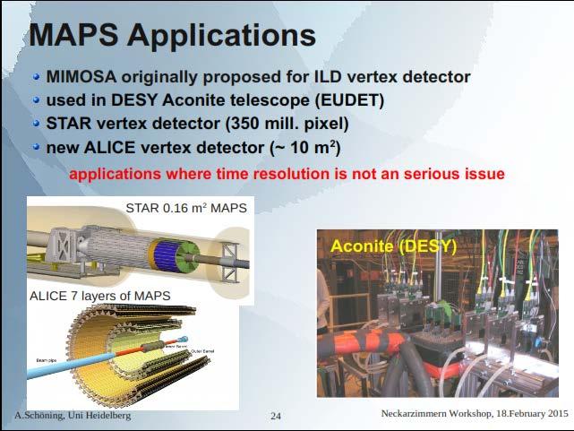
Application of CMOS sensors in radiation detection
|
|
|
- Clarence Armstrong
- 5 years ago
- Views:
Transcription


1 Application of CMOS sensors in radiation detection S. Ashrafi Physics Faculty University of Tabriz 1
2 CMOS is a technology for making low power integrated circuits. CMOS Complementary Metal Oxide Semiconductor MOS the MOSFET transistors Complimentary the two different types of semiconductors (N-type and P-type) CMOS is used in electronics: static RAM, digital logic circuits, micro processors, micro controllers, image sensors and particle tracking, and 2

3 Architecture of a CMOS image sensor access a pixel and read the signal value transistors photodetector 3
4 Basic functions of CMOS webcam: Optical gathering of photons (lens) Wavelength discrimination of photons (filter) Detector for photons to electrons conversion (photodiode) readout the detector Timing control, and drive electronics Signal processing electronics Analog-to digital conversion Interface electronics 4


5 Basic configuration of CMOS image sensor. M RS = reset transistor M SF = source follower transistor M SEL = select transistor An n-mosfet structure is shown: source is a PD drain is biased at V dd gate is off-state. 5


6 n MOSFET Potential profile electron density The impurity density in the source is smaller than that in the drain. Ohta
7 The operation of an APS is as follows: First, the reset transistor M RS is turned on. This resets V PD to (V dd V th ), where V th is the threshold voltage of transistor M RS. Then, M RS is turned off and the PD is electrically floated. When light is incident, the photo-generated carriers accumulate in the PD junction capacitance C PD. The accumulated charge decreases V PD according to the input light intensity. After an accumulation time of 33 msec, (at video rate), the select transistor M SEL is turned on and the output signal in the pixel is read out in the vertical output line. When the read-out process is finished, M SEL is turned off and M RS is again turned on to repeat the above process. 7

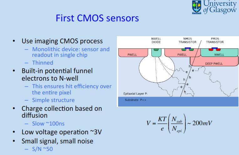
8 Photodetectors for CMOS image sensors behavior of minority carriers is important In p-type substrate minorities are electrons infrared (IR) penetrate up to 10 μm Diffusion of minorities to adjacent photodiodes image blurring. A PD is usually operated in accumulation mode. Photocarriers are swept to the surface due to the potential well in the depletion region Ohta-2007 The potential voltage decreases voltage drop the light power 8
9 9

10 Blooming The pixels potential well has got specified capacity. If quantity of charge is too large, then it diffuses into potential wells of surrounding pixels. 10
11 CMOS: pros & cons listing 1. Low power consumption. work at low voltage 2. Lower cost 4. Miniaturization 5. Random access of image data 6. High-speed imaging. 1. Lower Sensitivity Fill Factor Quantum Efficiency 2. Higher Noise especially under low illumination 3. Small Dynamic range Ratio: saturation signal / rms noise floor 11
12 Image sensor preparation for particle detection 3 He α p D T 12

13 Electron: range energy in Silicon 13


14 A Bayer filter over the pixel sensor array 2010-Holms 14
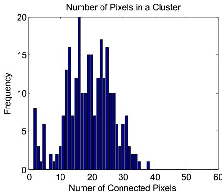
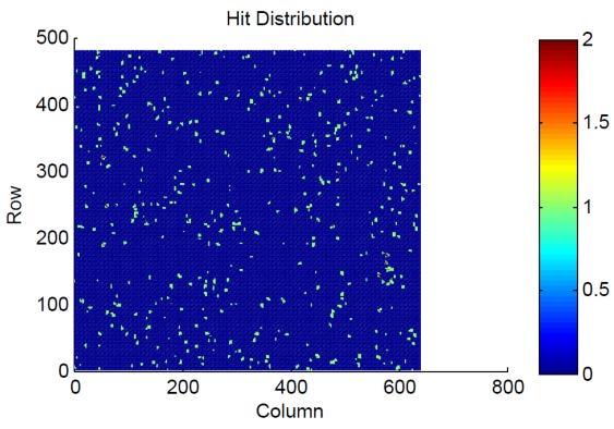
15 Camera Sensor Pixels with RGB Color and Infrared Blocking Filters 15
16 The back-illuminated BT sensor showed nearly 100% efficiency. computing the size, charge and coordinates of the center of each alpha cluster detected. Maneuski-2011 measurements in a light tight box 241 Am (activity 4.6 kbq) source 5.48 MeV alpha particles 16
 Sample is unbiased 3) Integration time is 3 seconds")
17 Total Ionizing Dose (TID) via Dark Current (DC) analysis 1) 60 Co irradiation at room temperature 2) Sample is unbiased 3) Integration time is 3 seconds 2010-Beaumel 17


18 GeigerCam: Measuring Radioactivity with Webcams use morphological clustering to group pixels into particle impact events and analyze their energies. Thomas Auzinger,

19 Dead time The frame rate was 30 Hz, but there were only six different frames per second gathered. It could be caused by large quantity of generated charge that could not be discharged by circuits in the image sensor. The dead time of this detector is 5 cycles, which corresponds to 1/ 6 s, compared to the dead time of Geiger-Müller counters of about 10 4 s 19
20 Radon monitor electrostatic concentrator 2013-Griffin 20
21 Radon measurements: β α 2013-Griffin 21
 For X-rays, the blue component has higher sensitivity")
22 Linearity & Sensitivity Sensor has a thickness of less than 10 μm 1) The excellent linearity 2) For X-rays, the blue component has higher sensitivity Kang
23 X-ray energy dependence Kang
24 Gamma-ray dose rate dependence 137 CS: 662 kev Kang

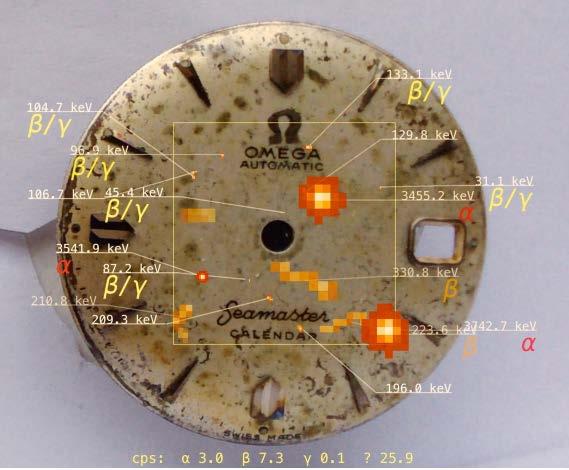
25 Other Gamma-rays Kang


26 CellRAD CellRAD is a system of software that runs on off-the-shelf unmodified Android cellphones. It uses the camera of the phone to detect gamma radiation. 26


27 Dark current distribution low dose CMOS CHARACTERISTICS Shift of distribution Due to TID Dark current spectroscopy: Second peak is related to deep-level traps 2014-Virmontois 27

28 Dark current distribution high dose Shift of distribution Due to TID Spikes are related to Displacement damages 2014-virmontois 28


29 CMOS image sensors as X-ray imagers 1 mm High-resolution X-ray micro-imaging X-ray beam monitor 2015-Castoldi 29


30 CMOS image sensors as particle beam monitors 1 up to 6 MeV proton beam Image of a single 1 MeV proton detection Castoldi 30

 Suppression")
31 The CMOS imager: Commercial APTINA MT9V011 Fixed Pattern Noise (FPN) Suppression -5σ 2015-Perez 31

: 662 kev 55")


32 Response of CMOS to γ, β rays and α particles 137 Cs(γ ray): 662 kev 55 Fe: 5.90 kev or 6.5 kev X-ray 137 Cs( β ray): 514, 1176 kev 2015-Perez 32


33 Response of CMOS to neutrons 2018-Prez 33


34 Am-241 α particle E= 5485, 5443, 5388 kev phosphorus-32 β particle E max = 1711 kev 2018-Nelson 34
35 Photodiode Sensor (PD) Monolithic Active Pixel Sensor (MAPS) Improved Fill factor Complementary Sensor Active Pixel sensor (CAPS) Improved Fill factor diffusion drift 35

36 A 4-T APS structure 2008-Rao 36
37 37
38 Disadvantages: 38
39 39
40 Complementary active pixels sensors (CAPS) 40

41 Complementary active pixels sensors (CAPS) The main new features are that the reset transistor is replaced by a PMOS. Apply bias voltage to bulk rely on drift instead of diffusion Take care of inter-pixel isolation Avoid charge collection on parasitic wells by shielding them inside a deep n-well 41

42 Pixelated Silicon as a sensor: Keller 42

43 Pixelated Silicon Keller 43

44 Pattern Recognition: Keller 44

45 different topology shapes detected with a CCD a high-energy proton ---- or a neutron-induced reaction with three ejected evaporation particles 2014-Saoud 45
46 Conclusions: CMOS sensors are applicable to: Radiation dosimetry Particle tracking Particle identification Beam monitoring X-ray imaging CMOS sensors are available at low cost (COTS) 46

47 47
48 References: Ohta, J. (2007). Smart CMOS image sensors and applications. CRC press. Holms, A., & Quach, A. (2010). Complementary Metal-Oxide Semiconductor Sensors. Maneuski, D., Blue, A., Hynds, D., Mac Raighne, A., & O'Shea, V. (2011). Evaluation of silicon active pixel sensors for alpha particle detection. Nuclear Instruments and Methods in Physics Research Section A: Accelerators, Spectrometers, Detectors and Associated Equipment, 659(1), Beaumel, M., Herve, D., & Van Aken, D. (2010). Cobalt-60, proton and electron irradiation of a radiation-hardened active pixel sensor. IEEE Transactions on Nuclear Science, 57(4), Auzinger, T., Habel, R., Musilek, A., Hainz, D., & Wimmer, M. (2012, August). GeigerCam: measuring radioactivity with webcams. In SIGGRAPH Posters (p. 40). 48
49 References: 49
50 Classical MAPS HV/HR-CMOS Apply bias voltage to bulk rely on drift instead of diffusion Avoid charge collection on parasitic wells by shielding them inside a deep n-well Take care of inter-pixel isolation after irradiation by suitable techniques Often a rather classical charge-sensitive amplifier with leakage current compensation is used at the expense of larger pixels New applications opening up? 50
51 51
52 52
Fundamentals of CMOS Image Sensors
 CHAPTER 2 Fundamentals of CMOS Image Sensors Mixed-Signal IC Design for Image Sensor 2-1 Outline Photoelectric Effect Photodetectors CMOS Image Sensor(CIS) Array Architecture CIS Peripherals Design Considerations
Simulation of High Resistivity (CMOS) Pixels
 Pixels") Simulation of High Resistivity (CMOS) Pixels Stefan Lauxtermann, Kadri Vural Sensor Creations Inc. AIDA-2020 CMOS Simulation Workshop May 13 th 2016 OUTLINE 1. Definition of High Resistivity Pixel Also
Simulation of High Resistivity (CMOS) Pixels Stefan Lauxtermann, Kadri Vural Sensor Creations Inc. AIDA-2020 CMOS Simulation Workshop May 13 th 2016 OUTLINE 1. Definition of High Resistivity Pixel Also
EVALUATION OF RADIATION HARDNESS DESIGN TECHNIQUES TO IMPROVE RADIATION TOLERANCE FOR CMOS IMAGE SENSORS DEDICATED TO SPACE APPLICATIONS
 EVALUATION OF RADIATION HARDNESS DESIGN TECHNIQUES TO IMPROVE RADIATION TOLERANCE FOR CMOS IMAGE SENSORS DEDICATED TO SPACE APPLICATIONS P. MARTIN-GONTHIER, F. CORBIERE, N. HUGER, M. ESTRIBEAU, C. ENGEL,
Fully depleted, thick, monolithic CMOS pixels with high quantum efficiency
 Fully depleted, thick, monolithic CMOS pixels with high quantum efficiency Andrew Clarke a*, Konstantin Stefanov a, Nicholas Johnston a and Andrew Holland a a Centre for Electronic Imaging, The Open University,
3084 IEEE TRANSACTIONS ON NUCLEAR SCIENCE, VOL. 60, NO. 4, AUGUST 2013
 3084 IEEE TRANSACTIONS ON NUCLEAR SCIENCE, VOL. 60, NO. 4, AUGUST 2013 Dummy Gate-Assisted n-mosfet Layout for a Radiation-Tolerant Integrated Circuit Min Su Lee and Hee Chul Lee Abstract A dummy gate-assisted
Design cycle for MEMS
 Design cycle for MEMS Design cycle for ICs IC Process Selection nmos CMOS BiCMOS ECL for logic for I/O and driver circuit for critical high speed parts of the system The Real Estate of a Wafer MOS Transistor
Semiconductor Detector Systems
 Semiconductor Detector Systems Helmuth Spieler Physics Division, Lawrence Berkeley National Laboratory OXFORD UNIVERSITY PRESS ix CONTENTS 1 Detector systems overview 1 1.1 Sensor 2 1.2 Preamplifier 3
Photons and solid state detection
 Photons and solid state detection Photons represent discrete packets ( quanta ) of optical energy Energy is hc/! (h: Planck s constant, c: speed of light,! : wavelength) For solid state detection, photons
In the name of God, the most merciful Electromagnetic Radiation Measurement
 In the name of God, the most merciful Electromagnetic Radiation Measurement In these slides, many figures have been taken from the Internet during my search in Google. Due to the lack of space and diversity
Evaluation of the Radiation Tolerance of Several Generations of SiGe Heterojunction Bipolar Transistors Under Radiation Exposure
 1 Evaluation of the Radiation Tolerance of Several Generations of SiGe Heterojunction Bipolar Transistors Under Radiation Exposure J. Metcalfe, D. E. Dorfan, A. A. Grillo, A. Jones, F. Martinez-McKinney,
A flexible compact readout circuit for SPAD arrays ABSTRACT Keywords: 1. INTRODUCTION 2. THE SPAD 2.1 Operation 7780C - 55
 A flexible compact readout circuit for SPAD arrays Danial Chitnis * and Steve Collins Department of Engineering Science University of Oxford Oxford England OX13PJ ABSTRACT A compact readout circuit that
VII. IR Arrays & Readout VIII.CCDs & Readout. This lecture course follows the textbook Detection of
 Detection of Light VII. IR Arrays & Readout VIII.CCDs & Readout This lecture course follows the textbook Detection of Light 4-3-2016 by George Rieke, Detection Cambridge of Light Bernhard Brandl University
Strip Detectors. Principal: Silicon strip detector. Ingrid--MariaGregor,SemiconductorsasParticleDetectors. metallization (Al) p +--strips
 p +--strips") Strip Detectors First detector devices using the lithographic capabilities of microelectronics First Silicon detectors -- > strip detectors Can be found in all high energy physics experiments of the last
Strip Detectors First detector devices using the lithographic capabilities of microelectronics First Silicon detectors -- > strip detectors Can be found in all high energy physics experiments of the last
MOSFET short channel effects
 MOSFET short channel effects overview Five different short channel effects can be distinguished: velocity saturation drain induced barrier lowering (DIBL) impact ionization surface scattering hot electrons
Fundamentals of Power Semiconductor Devices
 В. Jayant Baliga Fundamentals of Power Semiconductor Devices 4y Spri ringer Contents Preface vii Chapter 1 Introduction 1 1.1 Ideal and Typical Power Switching Waveforms 3 1.2 Ideal and Typical Power Device
Ultra-high resolution 14,400 pixel trilinear color image sensor
 Ultra-high resolution 14,400 pixel trilinear color image sensor Thomas Carducci, Antonio Ciccarelli, Brent Kecskemety Microelectronics Technology Division Eastman Kodak Company, Rochester, New York 14650-2008
Semiconductor Physics and Devices
 Metal-Semiconductor and Semiconductor Heterojunctions The Metal-Oxide-Semiconductor Field-Effect Transistor (MOSFET) is one of two major types of transistors. The MOSFET is used in digital circuit, because
Field-Effect Transistor (FET) is one of the two major transistors; FET derives its name from its working mechanism;
 is one of the two major transistors; FET derives its name from its working mechanism;") Chapter 3 Field-Effect Transistors (FETs) 3.1 Introduction Field-Effect Transistor (FET) is one of the two major transistors; FET derives its name from its working mechanism; The concept has been known
Chapter 3 Field-Effect Transistors (FETs) 3.1 Introduction Field-Effect Transistor (FET) is one of the two major transistors; FET derives its name from its working mechanism; The concept has been known
Electronic Radiation Hardening - Technology Demonstration Activities (TDAs)
") Electronic Radiation Hardening - Technology Demonstration Activities (TDAs) Véronique Ferlet-Cavrois ESA/ESTEC Acknowledgements to Ali Mohammadzadeh, Christian Poivey, Marc Poizat, Fredrick Sturesson ESA/ESTEC,
Electronic Radiation Hardening - Technology Demonstration Activities (TDAs) Véronique Ferlet-Cavrois ESA/ESTEC Acknowledgements to Ali Mohammadzadeh, Christian Poivey, Marc Poizat, Fredrick Sturesson ESA/ESTEC,
Development of the Pixelated Photon Detector. Using Silicon on Insulator Technology. for TOF-PET
 July 24, 2015 Development of the Pixelated Photon Detector Using Silicon on Insulator Technology for TOF-PET A.Koyama 1, K.Shimazoe 1, H.Takahashi 1, T. Orita 2, Y.Arai 3, I.Kurachi 3, T.Miyoshi 3, D.Nio
Threshold Voltage and Drain Current Investigation of Power MOSFET ZVN3320FTA by 2D Simulations
 Threshold Voltage and Drain Current Investigation of Power MOSFET ZVN3320FTA by 2D Simulations Ramani Kannan, Hesham Khalid Department of Electrical and Electronic Engineering Universiti Teknologi PETRONAS,
FUTURE PROSPECTS FOR CMOS ACTIVE PIXEL SENSORS
 FUTURE PROSPECTS FOR CMOS ACTIVE PIXEL SENSORS Dr. Eric R. Fossum Jet Propulsion Laboratory Dr. Philip H-S. Wong IBM Research 1995 IEEE Workshop on CCDs and Advanced Image Sensors April 21, 1995 CMOS APS
Military Performance Specifications
 RADIATION OWNER S MANUAL RHA-Related Documents Military Performance Specifications 19500 General Specification for Semiconductor Devices 38534 Performance Specifications for Hybrid Microcircuits 38535
Introduction. Chapter 1
 1 Chapter 1 Introduction During the last decade, imaging with semiconductor devices has been continuously replacing conventional photography in many areas. Among all the image sensors, the charge-coupled-device
Three Ways to Detect Light. We now establish terminology for photon detectors:
 Three Ways to Detect Light In photon detectors, the light interacts with the detector material to produce free charge carriers photon-by-photon. The resulting miniscule electrical currents are amplified
Monolithic Pixel Sensors in SOI technology R&D activities at LBNL
 Monolithic Pixel Sensors in SOI technology R&D activities at LBNL Lawrence Berkeley National Laboratory M. Battaglia, L. Glesener (UC Berkeley & LBNL), D. Bisello, P. Giubilato (LBNL & INFN Padova), P.
Design and Performance of a Pinned Photodiode CMOS Image Sensor Using Reverse Substrate Bias
 Design and Performance of a Pinned Photodiode CMOS Image Sensor Using Reverse Substrate Bias 13 September 2017 Konstantin Stefanov Contents Background Goals and objectives Overview of the work carried
FUNDAMENTALS OF MODERN VLSI DEVICES
 19-13- FUNDAMENTALS OF MODERN VLSI DEVICES YUAN TAUR TAK H. MING CAMBRIDGE UNIVERSITY PRESS Physical Constants and Unit Conversions List of Symbols Preface page xi xiii xxi 1 INTRODUCTION I 1.1 Evolution
Tests of monolithic CMOS SOI pixel detector prototype INTPIX3 MOHAMMED IMRAN AHMED. Supervisors Dr. Henryk Palka (IFJ-PAN) Dr. Marek Idzik(AGH-UST)
 Dr. Marek Idzik(AGH-UST)") Internal Note IFJ PAN Krakow (SOIPIX) Tests of monolithic CMOS SOI pixel detector prototype INTPIX3 by MOHAMMED IMRAN AHMED Supervisors Dr. Henryk Palka (IFJ-PAN) Dr. Marek Idzik(AGH-UST) Test and Measurement
Internal Note IFJ PAN Krakow (SOIPIX) Tests of monolithic CMOS SOI pixel detector prototype INTPIX3 by MOHAMMED IMRAN AHMED Supervisors Dr. Henryk Palka (IFJ-PAN) Dr. Marek Idzik(AGH-UST) Test and Measurement
DesignofaRad-HardLibraryof DigitalCellsforSpaceApplications
 DesignofaRad-HardLibraryof DigitalCellsforSpaceApplications Alberto Stabile, Valentino Liberali and Cristiano Calligaro stabile@dti.unimi.it, liberali@dti.unimi.it, c.calligaro@redcatdevices.it Department
Active Pixel Sensors Fabricated in a Standard 0.18 um CMOS Technology
 Active Pixel Sensors Fabricated in a Standard.18 um CMOS Technology Hui Tian, Xinqiao Liu, SukHwan Lim, Stuart Kleinfelder, and Abbas El Gamal Information Systems Laboratory, Stanford University Stanford,
Charge coupled CMOS and hybrid detector arrays
 Charge coupled CMOS and hybrid detector arrays James Janesick Sarnoff Corporation, 4952 Warner Ave., Suite 300, Huntington Beach, CA. 92649 Headquarters: CN5300, 201 Washington Road Princeton, NJ 08543-5300
Session 10: Solid State Physics MOSFET
 Session 10: Solid State Physics MOSFET 1 Outline A B C D E F G H I J 2 MOSCap MOSFET Metal-Oxide-Semiconductor Field-Effect Transistor: Al (metal) SiO2 (oxide) High k ~0.1 ~5 A SiO2 A n+ n+ p-type Si (bulk)
Lecture 18: Photodetectors
 Lecture 18: Photodetectors Contents 1 Introduction 1 2 Photodetector principle 2 3 Photoconductor 4 4 Photodiodes 6 4.1 Heterojunction photodiode.................... 8 4.2 Metal-semiconductor photodiode................
Overview. Charge-coupled Devices. MOS capacitor. Charge-coupled devices. Charge-coupled devices:
 Overview Charge-coupled Devices Charge-coupled devices: MOS capacitors Charge transfer Architectures Color Limitations 1 2 Charge-coupled devices MOS capacitor The most popular image recording technology
Amplifier Luminescence and RBI. Richard Crisp May 21,
 Amplifier Luminescence and RBI Richard Crisp May 21, 2013 rdcrisp@earthlink.net www.narrowbandimaging.com Outline What is amplifier luminescence? What mechanism causes amplifier luminescence at the transistor
STATE-OF-THE-ART SILICON DETECTORS FOR X-RAY SPECTROSCOPY
 Copyright JCPDS - International Centre for Diffraction Data 2004, Advances in X-ray Analysis, Volume 47. 47 STATE-OF-THE-ART SILICON DETECTORS FOR X-RAY SPECTROSCOPY P. Lechner* 1, R. Hartmann* 1, P. Holl*
ABSTRACT. Keywords: 0,18 micron, CMOS, APS, Sunsensor, Microned, TNO, TU-Delft, Radiation tolerant, Low noise. 1. IMAGERS FOR SPACE APPLICATIONS.
 Active pixel sensors: the sensor of choice for future space applications Johan Leijtens(), Albert Theuwissen(), Padmakumar R. Rao(), Xinyang Wang(), Ning Xie() () TNO Science and Industry, Postbus, AD
Cosmic Rays induced Single Event Effects in Power Semiconductor Devices
 Cosmic Rays induced Single Event Effects in Power Semiconductor Devices Giovanni Busatto University of Cassino ITALY Outline Introduction Cosmic rays in Space Cosmic rays at Sea Level Radiation Effects
Department of Electrical Engineering IIT Madras
 Department of Electrical Engineering IIT Madras Sample Questions on Semiconductor Devices EE3 applicants who are interested to pursue their research in microelectronics devices area (fabrication and/or
ABSTRACT. Section I Overview of the µdss
 An Autonomous Low Power High Resolution micro-digital Sun Sensor Ning Xie 1, Albert J.P. Theuwissen 1, 2 1. Delft University of Technology, Delft, the Netherlands; 2. Harvest Imaging, Bree, Belgium; ABSTRACT
Interpixel crosstalk in a 3D-integrated active pixel sensor for x-ray detection
 Interpixel crosstalk in a 3D-integrated active pixel sensor for x-ray detection The MIT Faculty has made this article openly available. Please share how this access benefits you. Your story matters. Citation
Soft X-Ray Silicon Photodiodes with 100% Quantum Efficiency
 PFC/JA-94-4 Soft X-Ray Silicon Photodiodes with 1% Quantum Efficiency K. W. Wenzel, C. K. Li, D. A. Pappas, Raj Kordel MIT Plasma Fusion Center Cambridge, Massachusetts 2139 USA March 1994 t Permanent
Highly Miniaturised Radiation Monitor (HMRM) Status Report. Yulia Bogdanova, Nicola Guerrini, Ben Marsh, Simon Woodward, Rain Irshad
 Status Report. Yulia Bogdanova, Nicola Guerrini, Ben Marsh, Simon Woodward, Rain Irshad") Highly Miniaturised Radiation Monitor (HMRM) Status Report Yulia Bogdanova, Nicola Guerrini, Ben Marsh, Simon Woodward, Rain Irshad HMRM programme aim Aim of phase A/B: Develop a chip sized prototype radiation
Highly Miniaturised Radiation Monitor (HMRM) Status Report Yulia Bogdanova, Nicola Guerrini, Ben Marsh, Simon Woodward, Rain Irshad HMRM programme aim Aim of phase A/B: Develop a chip sized prototype radiation
Semiconductor Memory: DRAM and SRAM. Department of Electrical and Computer Engineering, National University of Singapore
 Semiconductor Memory: DRAM and SRAM Outline Introduction Random Access Memory (RAM) DRAM SRAM Non-volatile memory UV EPROM EEPROM Flash memory SONOS memory QD memory Introduction Slow memories Magnetic
CCD30-11 NIMO Back Illuminated Deep Depleted High Performance CCD Sensor
 CCD30-11 NIMO Back Illuminated Deep Depleted High Performance CCD Sensor FEATURES 1024 by 256 Pixel Format 26µm Square Pixels Image area 26.6 x 6.7mm Back Illuminated format for high quantum efficiency
Radiation Induced Forward Emitter Current Gain Degradation of Lateral and Vertical PNP Power Transistors in Voltage Regulators
 1188 PIERS Proceedings, Xi an, China, March 22 26, 2010 Radiation Induced Forward Emitter Current Gain Degradation of Lateral and Vertical PNP Power Transistors in Voltage Regulators Vladimir Vukić 1 and
Detectors for microscopy - CCDs, APDs and PMTs. Antonia Göhler. Nov 2014
 Detectors for microscopy - CCDs, APDs and PMTs Antonia Göhler Nov 2014 Detectors/Sensors in general are devices that detect events or changes in quantities (intensities) and provide a corresponding output,
EE 392B: Course Introduction
 EE 392B Course Introduction About EE392B Goals Topics Schedule Prerequisites Course Overview Digital Imaging System Image Sensor Architectures Nonidealities and Performance Measures Color Imaging Recent
Lecture Notes 5 CMOS Image Sensor Device and Fabrication
 Lecture Notes 5 CMOS Image Sensor Device and Fabrication CMOS image sensor fabrication technologies Pixel design and layout Imaging performance enhancement techniques Technology scaling, industry trends
Depletion-mode operation ( 공핍형 ): Using an input gate voltage to effectively decrease the channel size of an FET
: Using an input gate voltage to effectively decrease the channel size of an FET") Ch. 13 MOSFET Metal-Oxide-Semiconductor Field-Effect Transistor : I D D-mode E-mode V g The gate oxide is made of dielectric SiO 2 with e = 3.9 Depletion-mode operation ( 공핍형 ): Using an input gate voltage
Ch. 13 MOSFET Metal-Oxide-Semiconductor Field-Effect Transistor : I D D-mode E-mode V g The gate oxide is made of dielectric SiO 2 with e = 3.9 Depletion-mode operation ( 공핍형 ): Using an input gate voltage
FET(Field Effect Transistor)
") Field Effect Transistor: Construction and Characteristic of JFETs. Transfer Characteristic. CS,CD,CG amplifier and analysis of CS amplifier MOSFET (Depletion and Enhancement) Type, Transfer Characteristic,
Field Effect Transistor: Construction and Characteristic of JFETs. Transfer Characteristic. CS,CD,CG amplifier and analysis of CS amplifier MOSFET (Depletion and Enhancement) Type, Transfer Characteristic,
A monolithic pixel sensor with fine space-time resolution based on silicon-on-insulator technology for the ILC vertex detector
 A monolithic pixel sensor with fine space-time resolution based on silicon-on-insulator technology for the ILC vertex detector, Miho Yamada, Toru Tsuboyama, Yasuo Arai, Ikuo Kurachi High Energy Accelerator
arxiv: v2 [physics.ins-det] 14 Jul 2015
![arxiv: v2 [physics.ins-det] 14 Jul 2015](/thumbs/77/76301481.jpg "arxiv: v2 [physics.ins-det] 14 Jul 2015") April 11, 2018 Compensation of radiation damages for SOI pixel detector via tunneling arxiv:1507.02797v2 [physics.ins-det] 14 Jul 2015 Miho Yamada 1, Yasuo Arai and Ikuo Kurachi Institute of Particle and
April 11, 2018 Compensation of radiation damages for SOI pixel detector via tunneling arxiv:1507.02797v2 [physics.ins-det] 14 Jul 2015 Miho Yamada 1, Yasuo Arai and Ikuo Kurachi Institute of Particle and
IOLTS th IEEE International On-Line Testing Symposium
 IOLTS 2018 24th IEEE International On-Line Testing Symposium Exp. comparison and analysis of the sensitivity to laser fault injection of CMOS FD-SOI and CMOS bulk technologies J.M. Dutertre 1, V. Beroulle
NAME: Last First Signature
 UNIVERSITY OF CALIFORNIA, BERKELEY College of Engineering Department of Electrical Engineering and Computer Sciences EE 130: IC Devices Spring 2003 FINAL EXAMINATION NAME: Last First Signature STUDENT
Digital Integrated Circuits A Design Perspective. The Devices. Digital Integrated Circuits 2nd Devices
 Digital Integrated Circuits A Design Perspective The Devices The Diode The diodes are rarely explicitly used in modern integrated circuits However, a MOS transistor contains at least two reverse biased
CMOS Detectors Ingeniously Simple!
 CMOS Detectors Ingeniously Simple! A.Schöning University Heidelberg B-Workshop Neckarzimmern 18.-20.2.2015 1 Detector System on Chip? 2 ATLAS Pixel Module 3 ATLAS Pixel Module MCC sensor FE-Chip FE-Chip
Demonstration of a Frequency-Demodulation CMOS Image Sensor
 Demonstration of a Frequency-Demodulation CMOS Image Sensor Koji Yamamoto, Keiichiro Kagawa, Jun Ohta, Masahiro Nunoshita Graduate School of Materials Science, Nara Institute of Science and Technology
Investigating the Causes of and Possible Remedies for Sensor Damage in Digital Cameras Used on the OMEGA Laser Systems.
 Investigating the Causes of and Possible Remedies for Sensor Damage in Digital Cameras Used on the OMEGA Laser Systems Krysta Boccuzzi Our Lady of Mercy High School Rochester, NY Advisor: Eugene Kowaluk
Image acquisition. In both cases, the digital sensing element is one of the following: Line array Area array. Single sensor
 Image acquisition Digital images are acquired by direct digital acquisition (digital still/video cameras), or scanning material acquired as analog signals (slides, photographs, etc.). In both cases, the
Module-3: Metal Oxide Semiconductor (MOS) & Emitter coupled logic (ECL) families
 & Emitter coupled logic (ECL) families") 1 Module-3: Metal Oxide Semiconductor (MOS) & Emitter coupled logic (ECL) families 1. Introduction 2. Metal Oxide Semiconductor (MOS) logic 2.1. Enhancement and depletion mode 2.2. NMOS and PMOS inverter
1 Module-3: Metal Oxide Semiconductor (MOS) & Emitter coupled logic (ECL) families 1. Introduction 2. Metal Oxide Semiconductor (MOS) logic 2.1. Enhancement and depletion mode 2.2. NMOS and PMOS inverter
Optical Receivers Theory and Operation
 Optical Receivers Theory and Operation Photo Detectors Optical receivers convert optical signal (light) to electrical signal (current/voltage) Hence referred O/E Converter Photodetector is the fundamental
Silicon Sensor Developments for the CMS Tracker Upgrade
 Silicon Sensor Developments for the CMS Tracker Upgrade on behalf of the CMS tracker collaboration University of Hamburg, Germany E-mail: Joachim.Erfle@desy.de CMS started a campaign to identify the future
Lawrence Berkeley National Laboratory Lawrence Berkeley National Laboratory
 Lawrence Berkeley National Laboratory Lawrence Berkeley National Laboratory Title Using an Active Pixel Sensor In A Vertex Detector Permalink https://escholarship.org/uc/item/5w19x8sx Authors Matis, Howard
Active Pixel Sensors Dr. Eric R. Fossum Jet Propulsion Laboratory, California Institute of Technology Pasadena, CA USA
 Active Pixel Sensors Dr. Eric R. Fossum Jet Propulsion Laboratory, California Institute of Technology Pasadena, CA 91109 USA A new type of image sensor is emerging from the most advanced image sensor R&D
UNIT 3: FIELD EFFECT TRANSISTORS
 FIELD EFFECT TRANSISTOR: UNIT 3: FIELD EFFECT TRANSISTORS The field effect transistor is a semiconductor device, which depends for its operation on the control of current by an electric field. There are
Lecture 2. Part 2 (Semiconductor detectors =sensors + electronics) Segmented detectors with pn-junction. Strip/pixel detectors
 Segmented detectors with pn-junction. Strip/pixel detectors") Lecture 2 Part 1 (Electronics) Signal formation Readout electronics Noise Part 2 (Semiconductor detectors =sensors + electronics) Segmented detectors with pn-junction Strip/pixel detectors Drift detectors
Lecture 2 Part 1 (Electronics) Signal formation Readout electronics Noise Part 2 (Semiconductor detectors =sensors + electronics) Segmented detectors with pn-junction Strip/pixel detectors Drift detectors
CONTENTS. 2.2 Schrodinger's Wave Equation 31. PART I Semiconductor Material Properties. 2.3 Applications of Schrodinger's Wave Equation 34
 CONTENTS Preface x Prologue Semiconductors and the Integrated Circuit xvii PART I Semiconductor Material Properties CHAPTER 1 The Crystal Structure of Solids 1 1.0 Preview 1 1.1 Semiconductor Materials
Week 7: Common-Collector Amplifier, MOS Field Effect Transistor
 EE 2110A Electronic Circuits Week 7: Common-Collector Amplifier, MOS Field Effect Transistor ecture 07-1 Topics to coer Common-Collector Amplifier MOS Field Effect Transistor Physical Operation and I-V
Charged Coupled Device (CCD) S.Vidhya
 S.Vidhya") Charged Coupled Device (CCD) S.Vidhya 02.04.2016 Sensor Physical phenomenon Sensor Measurement Output A sensor is a device that measures a physical quantity and converts it into a signal which can be read
Charged Coupled Device (CCD) S.Vidhya 02.04.2016 Sensor Physical phenomenon Sensor Measurement Output A sensor is a device that measures a physical quantity and converts it into a signal which can be read
Mechanis m Faliures. Group Leader Jepsy 1)Substrate Biasing 2) Minority Injection. Bob 1)Minority-Carrier Guard Rings
Substrate Biasing 2) Minority Injection. Bob 1)Minority-Carrier Guard Rings") Mechanis m Faliures Group Leader Jepsy 1)Substrate Biasing 2) Minority Injection As im 1)Types Of Guard Rings Sandra 1)Parasitics 2)Field Plating Bob 1)Minority-Carrier Guard Rings Shawn 1)Parasitic Channel
Mechanis m Faliures Group Leader Jepsy 1)Substrate Biasing 2) Minority Injection As im 1)Types Of Guard Rings Sandra 1)Parasitics 2)Field Plating Bob 1)Minority-Carrier Guard Rings Shawn 1)Parasitic Channel
Low Power Sensor Concepts
 Low Power Sensor Concepts Konstantin Stefanov 11 February 2015 Introduction The Silicon Pixel Tracker (SPT): The main driver is low detector mass Low mass is enabled by low detector power Benefits the
ECE 340 Lecture 37 : Metal- Insulator-Semiconductor FET Class Outline:
 ECE 340 Lecture 37 : Metal- Insulator-Semiconductor FET Class Outline: Metal-Semiconductor Junctions MOSFET Basic Operation MOS Capacitor Things you should know when you leave Key Questions What is the
A radiation-hardened optical receiver chip
 This article has been accepted and published on J-STAGE in advance of copyediting. Content is final as presented. A radiation-hardened optical receiver chip Xiao Zhou, Ping Luo a), Linyan He, Rongxun Ling
Sub-Threshold Region Behavior of Long Channel MOSFET
 Sub-threshold Region - So far, we have discussed the MOSFET behavior in linear region and saturation region - Sub-threshold region is refer to region where Vt is less than Vt - Sub-threshold region reflects
EFFECTS OF GAMMA RADIATION ON COMMERCIAL OPERATIONAL AMPLIFIERS
 009 International Nuclear Atlantic Conference - INAC 009 io de Janeiro,J, Brazil, September7 to October, 009 ASSOCIAÇÃO BASILEIA DE ENEGIA NUCLEA - ABEN ISBN: 978-85-994-03-8 EFFECTS OF GAMMA ADIATION
Lecture 7. July 24, Detecting light (converting light to electrical signal)
") Lecture 7 July 24, 2017 Detecting light (converting light to electrical signal) Photoconductor Photodiode Managing electrical signal Metal-oxide-semiconductor (MOS) capacitor Charge coupled device (CCD)
Lecture 7 July 24, 2017 Detecting light (converting light to electrical signal) Photoconductor Photodiode Managing electrical signal Metal-oxide-semiconductor (MOS) capacitor Charge coupled device (CCD)
ACTIVE PIXEL SENSORS VS. CHARGE-COUPLED DEVICES
 ACTIVE PIXEL SENSORS VS. CHARGE-COUPLED DEVICES Dr. Eric R. Fossum Imaging Systems Section Jet Propulsion Laboratory, California Institute of Technology (818) 354-3128 1993 IEEE Workshop on CCDs and Advanced
An Introduction to Scientific Imaging C h a r g e - C o u p l e d D e v i c e s
 p a g e 2 S C I E N T I F I C I M A G I N G T E C H N O L O G I E S, I N C. Introduction to the CCD F u n d a m e n t a l s The CCD Imaging A r r a y An Introduction to Scientific Imaging C h a r g e -
Radiation-tolerant CMOS APS Arrays
 JOURNAL INTEGRATED CIRCUITS AND SYSTEMS, VOL 1, NO. 3, JULY 2006. 17 Radiation-tolerant CMOS APS Arrays Vitor C. Dias da Silva, Leandro T. Dornelles, Pedro Paulo Canazio, Filipe V. dos Santos, A. Mesquita
Part I. CCD Image Sensors
 Part I CCD Image Sensors 2 Overview of CCD CCD is the abbreviation for charge-coupled device. CCD image sensors are silicon-based integrated circuits (ICs), consisting of a dense matrix of photodiodes
Characterisation of a Novel Reverse-Biased PPD CMOS Image Sensor
 Characterisation of a Novel Reverse-Biased PPD CMOS Image Sensor Konstantin D. Stefanov, Andrew S. Clarke, James Ivory and Andrew D. Holland Centre for Electronic Imaging, The Open University, Walton Hall,
Silicon sensors for radiant signals. D.Sc. Mikko A. Juntunen
 Silicon sensors for radiant signals D.Sc. Mikko A. Juntunen 2017 01 16 Today s outline Introduction Basic physical principles PN junction revisited Applications Light Ionizing radiation X-Ray sensors in
Detectors for Optical Communications
 Optical Communications: Circuits, Systems and Devices Chapter 3: Optical Devices for Optical Communications lecturer: Dr. Ali Fotowat Ahmady Sep 2012 Sharif University of Technology 1 Photo All detectors
Lecture Introduction
 Lecture 1 6.012 Introduction 1. Overview of 6.012 Outline 2. Key conclusions of 6.012 Reading Assignment: Howe and Sodini, Chapter 1 6.012 Electronic Devices and Circuits-Fall 200 Lecture 1 1 Overview
Q1. Explain the construction and principle of operation of N-Channel and P-Channel Junction Field Effect Transistor (JFET).
.") Q. Explain the construction and principle of operation of N-Channel and P-Channel Junction Field Effect Transistor (JFET). Answer: N-Channel Junction Field Effect Transistor (JFET) Construction: Drain(D)
Q. Explain the construction and principle of operation of N-Channel and P-Channel Junction Field Effect Transistor (JFET). Answer: N-Channel Junction Field Effect Transistor (JFET) Construction: Drain(D)
arxiv: v1 [physics.ins-det] 21 Jul 2015
![arxiv: v1 [physics.ins-det] 21 Jul 2015](/thumbs/96/128765305.jpg "arxiv: v1 [physics.ins-det] 21 Jul 2015") July 22, 2015 Compensation for TID Damage in SOI Pixel Devices arxiv:1507.05860v1 [physics.ins-det] 21 Jul 2015 Naoshi Tobita A, Shunsuke Honda A, Kazuhiko Hara A, Wataru Aoyagi A, Yasuo Arai B, Toshinobu
July 22, 2015 Compensation for TID Damage in SOI Pixel Devices arxiv:1507.05860v1 [physics.ins-det] 21 Jul 2015 Naoshi Tobita A, Shunsuke Honda A, Kazuhiko Hara A, Wataru Aoyagi A, Yasuo Arai B, Toshinobu
MEASUREMENT OF TIMEPIX DETECTOR PERFORMANCE VICTOR GUTIERREZ DIEZ UNIVERSIDAD COMPLUTENSE DE MADRID
 MEASUREMENT OF TIMEPIX DETECTOR PERFORMANCE VICTOR GUTIERREZ DIEZ UNIVERSIDAD COMPLUTENSE DE MADRID ABSTRACT Recent advances in semiconductor technology allow construction of highly efficient and low noise
The RADFET: TRANSDUCERS RESEARCH Transducers Group
 Page 1 of 5 TRANSDUCERS RESEARCH Transducers Group Introduction Research Teams Analog and Sensor Interface BioAnalytical Microsystems Chemical Microanalytics e-learning Instrumentation and software development,
Power MOSFET Zheng Yang (ERF 3017,
 ECE442 Power Semiconductor Devices and Integrated Circuits Power MOSFET Zheng Yang (ERF 3017, email: yangzhen@uic.edu) Evolution of low-voltage (
Research Article Responsivity Enhanced NMOSFET Photodetector Fabricated by Standard CMOS Technology
 Advances in Condensed Matter Physics Volume 2015, Article ID 639769, 5 pages http://dx.doi.org/10.1155/2015/639769 Research Article Responsivity Enhanced NMOSFET Photodetector Fabricated by Standard CMOS
Characterisation of SiPM Index :
 Characterisation of SiPM --------------------------------------------------------------------------------------------Index : 1. Basics of SiPM* 2. SiPM module 3. Working principle 4. Experimental setup
IT FR R TDI CCD Image Sensor
 4k x 4k CCD sensor 4150 User manual v1.0 dtd. August 31, 2015 IT FR 08192 00 R TDI CCD Image Sensor Description: With the IT FR 08192 00 R sensor ANDANTA GmbH builds on and expands its line of proprietary
Lecture 4. MOS transistor theory
 Lecture 4 MOS transistor theory 1.7 Introduction: A MOS transistor is a majority-carrier device, in which the current in a conducting channel between the source and the drain is modulated by a voltage
ELEN6350. Summary: High Dynamic Range Photodetector Hassan Eddrees, Matt Bajor
 ELEN6350 High Dynamic Range Photodetector Hassan Eddrees, Matt Bajor Summary: The use of image sensors presents several limitations for visible light spectrometers. Both CCD and CMOS one dimensional imagers
A STUDY OF THE RESPONSE OF DEPLETED TYPE p-mosfets TO PHOTON AND ELECTRON DOSE
 A STUDY OF THE RESPONSE OF DEPLETED TYPE p-mosfets TO PHOTON AND ELECTRON DOSE M. Fragopoulou 1, S. Stoulos 1, and M. Zamani 1, 1 School of Physics, Nuclear and Elementary Particle Section Aristotle University
Radiation hardened CMOS Image Sensors Development
 Radiation hardened CMOS Image Sensors Development Vincent Goiffon, ISAE-SUPAERO, Université de Toulouse, France CERN Radiation Working Group meeting 2017, April 13th Outline ISAE-SUPAERO Image Sensor Research
A new Vertical JFET Technology for Harsh Radiation Applications
 A New Vertical JFET Technology for Harsh Radiation Applications ISPS 2016 1 A new Vertical JFET Technology for Harsh Radiation Applications A Rad-Hard switch for the ATLAS Inner Tracker P. Fernández-Martínez,
 Electronic Devices 1. Current flowing in each of the following circuits A and respectively are: (Circuit 1) (Circuit 2) 1) 1A, 2A 2) 2A, 1A 3) 4A, 2A 4) 2A, 4A 2. Among the following one statement is not