Charged Coupled Device (CCD) S.Vidhya
|
|
|
- Melinda Hicks
- 5 years ago
- Views:
Transcription
1 Charged Coupled Device (CCD) S.Vidhya
2 Sensor Physical phenomenon Sensor Measurement Output A sensor is a device that measures a physical quantity and converts it into a signal which can be read by an observer or by an instrument. For example, a thermocouple converts temperature to an output voltage which can be read by a voltmeter. For accuracy, all sensors need to be calibrated against known standards
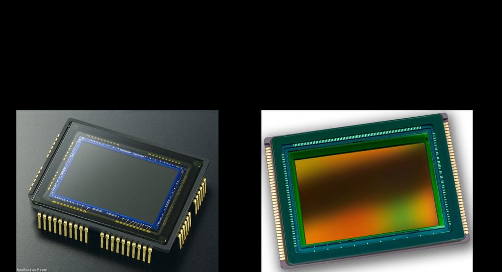
3 Image Sensor An image sensor is a device that converts an optical image into an electrical signal. Unlike traditional camera, that use film to capture and store an image, digital cameras use solid-state device called image sensor. Image sensors contain millions of photosensitive diodes known as photo sites. When you take a picture, the camera's shutter opens briefly and each photo site on the image sensor records the brightness of the light that falls on it by accumulating photons. The more light that hits a photo site, the more photons it records.

4 History Before 1960 mainly film photography was done and vacuum tubes were being used. From early research and development was done in the fields of CCD and CMOS. From commercialization of CCD took place. After 1990 re-emergence of CMOS took place and amorphous Si also came into the picture Nobel Prize in Physics
5


6 Charged Coupled Device (CCD) Charge-coupled devices (CCDs) are silicon-based integrated circuits consisting of a dense matrix of photodiodes that operate by converting light energy in the form of photons into an electronic charge. Electrons generated by the interaction of photons with silicon atoms are stored in a potential well and can subsequently be transferred across the chip through registers and output to an amplifier.
7 A CCD is a two-dimensional array of metal-oxidesemiconductor (MOS) capacitors. The charges are stored in the depletion region of the MOS capacitors. Charges are moved in the CCD circuit by manipulating the voltages on the gates of the capacitors so as to allow the charge to spill from one capacitor to the next (thus the name charge-coupled device). An amplifier provides an output voltage that can be processed. The CCD is a serial device where charge packets are read one at a time.
, causing each capacitor to accumulate an electric charge proportional to the light intensity at that location.")
8 Basic Operation of a CCD In a CCD for capturing images, there is a photoactive region, and a transmission region made out of a shift register (the CCD, properly speaking). An image is projected by a lens on the capacitor array (the photoactive region), causing each capacitor to accumulate an electric charge proportional to the light intensity at that location. A one-dimensional array, used in cameras, captures a single slice of the image, while a two-dimensional array, used in video and still cameras, captures a two-dimensional picture corresponding to the scene projected onto the focal plane of the sensor.
9 CCD Performance Categories Charge generation Quantum Efficiency (QE), Dark Current Charge collection full well capacity, pixels size, pixel uniformity, defects, diffusion (Modulation Transfer Function, MTF) Charge transfer Charge transfer efficiency (CTE), Defects Charge detection Readout Noise (RON), linearity 9

 per transfer of 0.")
10 Charge Transfer Efficiency Charge Transfer Efficiency is the fraction of electrons transferred from one pixel to the next When the wells are nearly empty, charge can be trapped by impurities in the silicon. So faint images can have tails in the vertical direction. Modern CCDs can have a charge transfer efficiency (CTE) per transfer of , so after 2000 transfers only 0.1% of the charge is lost. good CTE bad CTE

11 Defects: Dark Columns Dark columns: caused by traps that block the vertical transfer of charge during image readout. Traps can be caused by crystal boundaries in the silicon of the CCD or by manufacturing defects. Although they spoil the chip cosmetically, dark columns are not a big problem (removed by calibration).

12 Defects: Bright Columns Bright Column Cluster of Hot Spots Cosmic rays Bright columns are also caused by traps. Electrons contained in such traps can leak out during readout causing a vertical streak. Hot Spots are pixels with higher than normal dark current. Their brightness increases linearly with exposure times Somewhat rarer are light-emitting defects which are hot spots that act as tiny LEDS and cause a halo of light on the chip.


13 Fungal growth on camera & instrument lens

14 Be stubborn about your goals, & flexible about your methods. Thank you
CHARGE-COUPLED DEVICE (CCD)
") CHARGE-COUPLED DEVICE (CCD) Definition A charge-coupled device (CCD) is an analog shift register, enabling analog signals, usually light, manipulation - for example, conversion into a digital value that
CHARGE-COUPLED DEVICE (CCD) Definition A charge-coupled device (CCD) is an analog shift register, enabling analog signals, usually light, manipulation - for example, conversion into a digital value that
Image Formation and Capture. Acknowledgment: some figures by B. Curless, E. Hecht, W.J. Smith, B.K.P. Horn, and A. Theuwissen
 Image Formation and Capture Acknowledgment: some figures by B. Curless, E. Hecht, W.J. Smith, B.K.P. Horn, and A. Theuwissen Image Formation and Capture Real world Optics Sensor Devices Sources of Error
Overview. Charge-coupled Devices. MOS capacitor. Charge-coupled devices. Charge-coupled devices:
 Overview Charge-coupled Devices Charge-coupled devices: MOS capacitors Charge transfer Architectures Color Limitations 1 2 Charge-coupled devices MOS capacitor The most popular image recording technology
Photons and solid state detection
 Photons and solid state detection Photons represent discrete packets ( quanta ) of optical energy Energy is hc/! (h: Planck s constant, c: speed of light,! : wavelength) For solid state detection, photons
Properties of a Detector
 Properties of a Detector Quantum Efficiency fraction of photons detected wavelength and spatially dependent Dynamic Range difference between lowest and highest measurable flux Linearity detection rate
CCDS. Lesson I. Wednesday, August 29, 12
 CCDS Lesson I CCD OPERATION The predecessor of the CCD was a device called the BUCKET BRIGADE DEVICE developed at the Phillips Research Labs The BBD was an analog delay line, made up of capacitors such
Detectors for microscopy - CCDs, APDs and PMTs. Antonia Göhler. Nov 2014
 Detectors for microscopy - CCDs, APDs and PMTs Antonia Göhler Nov 2014 Detectors/Sensors in general are devices that detect events or changes in quantities (intensities) and provide a corresponding output,
The Charge-Coupled Device. Many overheads courtesy of Simon Tulloch
 The Charge-Coupled Device Astronomy 1263 Many overheads courtesy of Simon Tulloch smt@ing.iac.es Jan 24, 2013 What does a CCD Look Like? The fine surface electrode structure of a thick CCD is clearly visible
Introduction. Chapter 1
 1 Chapter 1 Introduction During the last decade, imaging with semiconductor devices has been continuously replacing conventional photography in many areas. Among all the image sensors, the charge-coupled-device
CCD Characteristics Lab
 CCD Characteristics Lab Observational Astronomy 6/6/07 1 Introduction In this laboratory exercise, you will be using the Hirsch Observatory s CCD camera, a Santa Barbara Instruments Group (SBIG) ST-8E.
An Introduction to CCDs. The basic principles of CCD Imaging is explained.
 An Introduction to CCDs. The basic principles of CCD Imaging is explained. Morning Brain Teaser What is a CCD? Charge Coupled Devices (CCDs), invented in the 1970s as memory devices. They improved the
STA3600A 2064 x 2064 Element Image Area CCD Image Sensor
 ST600A 2064 x 2064 Element Image Area CCD Image Sensor FEATURES 2064 x 2064 CCD Image Array 15 m x 15 m Pixel 30.96 mm x 30.96 mm Image Area Near 100% Fill Factor Readout Noise Less Than 3 Electrons at
STA1600LN x Element Image Area CCD Image Sensor
 ST600LN 10560 x 10560 Element Image Area CCD Image Sensor FEATURES 10560 x 10560 Photosite Full Frame CCD Array 9 m x 9 m Pixel 95.04mm x 95.04mm Image Area 100% Fill Factor Readout Noise 2e- at 50kHz
Charged-Coupled Devices
 Charged-Coupled Devices Charged-Coupled Devices Useful texts: Handbook of CCD Astronomy Steve Howell- Chapters 2, 3, 4.4 Measuring the Universe George Rieke - 3.1-3.3, 3.6 CCDs CCDs were invented in 1969
Fundamentals of CMOS Image Sensors
 CHAPTER 2 Fundamentals of CMOS Image Sensors Mixed-Signal IC Design for Image Sensor 2-1 Outline Photoelectric Effect Photodetectors CMOS Image Sensor(CIS) Array Architecture CIS Peripherals Design Considerations
Introduction to CCD camera
 Observational Astronomy 2011/2012 Introduction to CCD camera Charge Coupled Device (CCD) photo sensor coupled to shift register Jörg R. Hörandel Radboud University Nijmegen http://particle.astro.ru.nl/goto.html?astropract1-1112
Image Formation and Capture
 Figure credits: B. Curless, E. Hecht, W.J. Smith, B.K.P. Horn, A. Theuwissen, and J. Malik Image Formation and Capture COS 429: Computer Vision Image Formation and Capture Real world Optics Sensor Devices
Topic 9 - Sensors Within
 Topic 9 - Sensors Within Learning Outcomes In this topic, we will take a closer look at sensor sizes in digital cameras. By the end of this video you will have a better understanding of what the various
Three Ways to Detect Light. We now establish terminology for photon detectors:
 Three Ways to Detect Light In photon detectors, the light interacts with the detector material to produce free charge carriers photon-by-photon. The resulting miniscule electrical currents are amplified
KAF E. 512(H) x 512(V) Pixel. Enhanced Response. Full-Frame CCD Image Sensor. Performance Specification. Eastman Kodak Company
 x 512(V) Pixel. Enhanced Response. Full-Frame CCD Image Sensor. Performance Specification. Eastman Kodak Company") KAF - 0261E 512(H) x 512(V) Pixel Enhanced Response Full-Frame CCD Image Sensor Performance Specification Eastman Kodak Company Image Sensor Solutions Rochester, New York 14650 Revision 2 December 21,
KAF - 0261E 512(H) x 512(V) Pixel Enhanced Response Full-Frame CCD Image Sensor Performance Specification Eastman Kodak Company Image Sensor Solutions Rochester, New York 14650 Revision 2 December 21,
Digital camera. Sensor. Memory card. Circuit board
 Digital camera Circuit board Memory card Sensor Detector element (pixel). Typical size: 2-5 m square Typical number: 5-20M Pixel = Photogate Photon + Thin film electrode (semi-transparent) Depletion volume
Last class. This class. CCDs Fancy CCDs. Camera specs scmos
 CCDs and scmos Last class CCDs Fancy CCDs This class Camera specs scmos Fancy CCD cameras: -Back thinned -> higher QE -Unexposed chip -> frame transfer -Electron multiplying -> higher SNR -Fancy ADC ->
IT FR R TDI CCD Image Sensor
 4k x 4k CCD sensor 4150 User manual v1.0 dtd. August 31, 2015 IT FR 08192 00 R TDI CCD Image Sensor Description: With the IT FR 08192 00 R sensor ANDANTA GmbH builds on and expands its line of proprietary
Based on lectures by Bernhard Brandl
 Astronomische Waarneemtechnieken (Astronomical Observing Techniques) Based on lectures by Bernhard Brandl Lecture 10: Detectors 2 1. CCD Operation 2. CCD Data Reduction 3. CMOS devices 4. IR Arrays 5.
CCD reductions techniques
 CCD reductions techniques Origin of noise Noise: whatever phenomena that increase the uncertainty or error of a signal Origin of noises: 1. Poisson fluctuation in counting photons (shot noise) 2. Pixel-pixel
a simple optical imager
 Imagers and Imaging a simple optical imager Here s one on our 61-Inch Telescope Here s one on our 61-Inch Telescope filter wheel in here dewar preamplifier However, to get a large field we cannot afford
Basic principles of photography. David Capel 346B IST
 Basic principles of photography David Capel 346B IST Latin Camera Obscura = Dark Room Light passing through a small hole produces an inverted image on the opposite wall Safely observing the solar eclipse
Digital Imaging Rochester Institute of Technology
 Digital Imaging 1999 Rochester Institute of Technology So Far... camera AgX film processing image AgX photographic film captures image formed by the optical elements (lens). Unfortunately, the processing
Pocket Pumped Image Analysis Ivan Kotov Brookhaven National Laboratory
 Pocket Pumped Image Analysis Ivan Kotov Brookhaven National Laboratory Instrumentation Division Seminar November 13, 2013 1 CCD Readout Architecture Terms Charge motion Image area (exposed to light) Parallel
VII. IR Arrays & Readout VIII.CCDs & Readout. This lecture course follows the textbook Detection of
 Detection of Light VII. IR Arrays & Readout VIII.CCDs & Readout This lecture course follows the textbook Detection of Light 4-3-2016 by George Rieke, Detection Cambridge of Light Bernhard Brandl University
Image acquisition. In both cases, the digital sensing element is one of the following: Line array Area array. Single sensor
 Image acquisition Digital images are acquired by direct digital acquisition (digital still/video cameras), or scanning material acquired as analog signals (slides, photographs, etc.). In both cases, the
Advanced Camera and Image Sensor Technology. Steve Kinney Imaging Professional Camera Link Chairman
 Advanced Camera and Image Sensor Technology Steve Kinney Imaging Professional Camera Link Chairman Content Physical model of a camera Definition of various parameters for EMVA1288 EMVA1288 and image quality
Image Sensor Characterization in a Photographic Context
 Image Sensor Characterization in a Photographic Context Sean C. Kelly, Gloria G. Putnam, Richard B. Wheeler, Shen Wang, William Davis, Ed Nelson, and Doug Carpenter Eastman Kodak Company Rochester, New
Lecture 30: Image Sensors (Cont) Computer Graphics and Imaging UC Berkeley CS184/284A
 Computer Graphics and Imaging UC Berkeley CS184/284A") Lecture 30: Image Sensors (Cont) Computer Graphics and Imaging UC Berkeley Reminder: The Pixel Stack Microlens array Color Filter Anti-Reflection Coating Stack height 4um is typical Pixel size 2um is typical
Lecture 30: Image Sensors (Cont) Computer Graphics and Imaging UC Berkeley Reminder: The Pixel Stack Microlens array Color Filter Anti-Reflection Coating Stack height 4um is typical Pixel size 2um is typical
Integrated Multi-Aperture Imaging
 Integrated Multi-Aperture Imaging Keith Fife, Abbas El Gamal, Philip Wong Department of Electrical Engineering, Stanford University, Stanford, CA 94305 1 Camera History 2 Camera History Despite progress,
Charge-Coupled Device (CCD) Detectors pixel silicon chip electronics cryogenics
 Detectors pixel silicon chip electronics cryogenics") Charge-Coupled Device (CCD) Detectors As revolutionary in astronomy as the invention of the telescope and photography semiconductor detectors a collection of miniature photodiodes, each called a picture
Charge-Coupled Device (CCD) Detectors As revolutionary in astronomy as the invention of the telescope and photography semiconductor detectors a collection of miniature photodiodes, each called a picture
LENSES. INEL 6088 Computer Vision
 LENSES INEL 6088 Computer Vision Digital camera A digital camera replaces film with a sensor array Each cell in the array is a Charge Coupled Device light-sensitive diode that converts photons to electrons
Astro-photography. Daguerreotype: on a copper plate
 AST 1022L Astro-photography 1840-1980s: Photographic plates were astronomers' main imaging tool At right: first ever picture of the full moon, by John William Draper (1840) Daguerreotype: exposure using
What an Observational Astronomer needs to know!
 What an Observational Astronomer needs to know! IRAF:Photometry D. Hatzidimitriou Masters course on Methods of Observations and Analysis in Astronomy Basic concepts Counts how are they related to the actual
CCD Analogy BUCKETS (PIXELS) HORIZONTAL CONVEYOR BELT (SERIAL REGISTER) VERTICAL CONVEYOR BELTS (CCD COLUMNS) RAIN (PHOTONS)
 HORIZONTAL CONVEYOR BELT (SERIAL REGISTER) VERTICAL CONVEYOR BELTS (CCD COLUMNS) RAIN (PHOTONS)") CCD Analogy RAIN (PHOTONS) VERTICAL CONVEYOR BELTS (CCD COLUMNS) BUCKETS (PIXELS) HORIZONTAL CONVEYOR BELT (SERIAL REGISTER) MEASURING CYLINDER (OUTPUT AMPLIFIER) Exposure finished, buckets now contain
CCD Analogy RAIN (PHOTONS) VERTICAL CONVEYOR BELTS (CCD COLUMNS) BUCKETS (PIXELS) HORIZONTAL CONVEYOR BELT (SERIAL REGISTER) MEASURING CYLINDER (OUTPUT AMPLIFIER) Exposure finished, buckets now contain
Camera Test Protocol. Introduction TABLE OF CONTENTS. Camera Test Protocol Technical Note Technical Note
 Technical Note CMOS, EMCCD AND CCD CAMERAS FOR LIFE SCIENCES Camera Test Protocol Introduction The detector is one of the most important components of any microscope system. Accurate detector readings
Silicon sensors for radiant signals. D.Sc. Mikko A. Juntunen
 Silicon sensors for radiant signals D.Sc. Mikko A. Juntunen 2017 01 16 Today s outline Introduction Basic physical principles PN junction revisited Applications Light Ionizing radiation X-Ray sensors in
Getting light to imager. Capturing Images. Depth and Distance. Ideal Imaging. CS559 Lecture 2 Lights, Cameras, Eyes
 CS559 Lecture 2 Lights, Cameras, Eyes Last time: what is an image idea of image-based (raster representation) Today: image capture/acquisition, focus cameras and eyes displays and intensities Corrected
Pixel CCD RASNIK. Kevan S Hashemi and James R Bensinger Brandeis University May 1997
 ATLAS Internal Note MUON-No-180 Pixel CCD RASNIK Kevan S Hashemi and James R Bensinger Brandeis University May 1997 Introduction This note compares the performance of the established Video CCD version
Where detectors are used in science & technology
 Lecture 9 Outline Role of detectors Photomultiplier tubes (photoemission) Modulation transfer function Photoconductive detector physics Detector architecture Where detectors are used in science & technology
Optical/IR Observational Astronomy Detectors II. David Buckley, SAAO
 David Buckley, SAAO 1 The Next Revolution: Charge Couple Device Detectors (CCDs) 2 Optical/IR Observational Astronomy CCDs Integrated semi-conductor detector From photon detection (pair production) to
CCD1600A Full Frame CCD Image Sensor x Element Image Area
 - 1 - General Description CCD1600A Full Frame CCD Image Sensor 10560 x 10560 Element Image Area General Description The CCD1600 is a 10560 x 10560 image element solid state Charge Coupled Device (CCD)
ISIS2 as a Pixel Sensor for ILC
 ISIS2 as a Pixel Sensor for ILC Yiming Li (University of Oxford) on behalf of UK ISIS Collaboration (U. Oxford, RAL, Open University) LCWS 10 Beijing, 28th March 2010 1 / 24 Content Introduction to ISIS
University Of Lübeck ISNM Presented by: Omar A. Hanoun
 University Of Lübeck ISNM 12.11.2003 Presented by: Omar A. Hanoun What Is CCD? Image Sensor: solid-state device used in digital cameras to capture and store an image. Photosites: photosensitive diodes
brief history of photography foveon X3 imager technology description
 brief history of photography foveon X3 imager technology description imaging technology 30,000 BC chauvet-pont-d arc pinhole camera principle first described by Aristotle fourth century B.C. oldest known
VC 14/15 TP2 Image Formation
 VC 14/15 TP2 Image Formation Mestrado em Ciência de Computadores Mestrado Integrado em Engenharia de Redes e Sistemas Informáticos Miguel Tavares Coimbra Outline Computer Vision? The Human Visual System
Megapixels and more. The basics of image processing in digital cameras. Construction of a digital camera
 Megapixels and more The basics of image processing in digital cameras Photography is a technique of preserving pictures with the help of light. The first durable photograph was made by Nicephor Niepce
PRELIMINARY. CCD 3041 Back-Illuminated 2K x 2K Full Frame CCD Image Sensor FEATURES
 CCD 3041 Back-Illuminated 2K x 2K Full Frame CCD Image Sensor FEATURES 2048 x 2048 Full Frame CCD 15 µm x 15 µm Pixel 30.72 mm x 30.72 mm Image Area 100% Fill Factor Back Illuminated Multi-Pinned Phase
Lens Aperture. South Pasadena High School Final Exam Study Guide- 1 st Semester Photo ½. Study Guide Topics that will be on the Final Exam
 South Pasadena High School Final Exam Study Guide- 1 st Semester Photo ½ Study Guide Topics that will be on the Final Exam The Rule of Thirds Depth of Field Lens and its properties Aperture and F-Stop
KAF-3200E / KAF-3200ME
 KAF- 3200E KAF- 3200ME 2184 (H) x 1472 () Pixel Full-Frame CCD Image Sensor Performance Specification Eastman Kodak Company Image Sensor Solutions Rochester, New York 14650-2010 Revision 1 September 26,
CCD Requirements for Digital Photography
 IS&T's 2 PICS Conference IS&T's 2 PICS Conference Copyright 2, IS&T CCD Requirements for Digital Photography Richard L. Baer Hewlett-Packard Laboratories Palo Alto, California Abstract The performance
The. FIES Camera. equipped with E2V CCD B83, ser. no Pre-commissioning characterisation
 The FIES Camera equipped with E2V CCD42-40-1-B83, ser. no. 01064-17-04 Pre-commissioning characterisation Anton Norup Sørensen Copenhagen University Observatory October 2003 Contents 1 Introduction 2 2
Cameras CS / ECE 181B
 Cameras CS / ECE 181B Image Formation Geometry of image formation (Camera models and calibration) Where? Radiometry of image formation How bright? What color? Examples of cameras What is a Camera? A camera
An Introduction to Scientific Imaging C h a r g e - C o u p l e d D e v i c e s
 p a g e 2 S C I E N T I F I C I M A G I N G T E C H N O L O G I E S, I N C. Introduction to the CCD F u n d a m e n t a l s The CCD Imaging A r r a y An Introduction to Scientific Imaging C h a r g e -
Acquisition. Some slides from: Yung-Yu Chuang (DigiVfx) Jan Neumann, Pat Hanrahan, Alexei Efros
 Jan Neumann, Pat Hanrahan, Alexei Efros") Acquisition Some slides from: Yung-Yu Chuang (DigiVfx) Jan Neumann, Pat Hanrahan, Alexei Efros Image Acquisition Digital Camera Film Outline Pinhole camera Lens Lens aberrations Exposure Sensors Noise
Acquisition Some slides from: Yung-Yu Chuang (DigiVfx) Jan Neumann, Pat Hanrahan, Alexei Efros Image Acquisition Digital Camera Film Outline Pinhole camera Lens Lens aberrations Exposure Sensors Noise
Three Ways to Detect Light. Following: Lord Rosse image of M33 vs. Hubble image demonstrate how critical detector technology is.
 Three Ways to Detect Light In photon detectors, the light interacts with the detector material to produce free charge carriers photon-by-photon. The resulting miniscule electrical currents are amplified
Light. Path of Light. Looking at things. Depth and Distance. Getting light to imager. CS559 Lecture 2 Lights, Cameras, Eyes
 CS559 Lecture 2 Lights, Cameras, Eyes These are course notes (not used as slides) Written by Mike Gleicher, Sept. 2005 Adjusted after class stuff we didn t get to removed / mistakes fixed Light Electromagnetic
3/5/17. Detector Basics. Quantum Efficiency (QE) and Spectral Response. Quantum Efficiency (QE) and Spectral Response
 and Spectral Response. Quantum Efficiency (QE) and Spectral Response") 3/5/17 Detector Basics The purpose of any detector is to record the light collected by the telescope. All detectors transform the incident radiation into a some other form to create a permanent record,
3/5/17 Detector Basics The purpose of any detector is to record the light collected by the telescope. All detectors transform the incident radiation into a some other form to create a permanent record,
The Noise about Noise
 The Noise about Noise I have found that few topics in astrophotography cause as much confusion as noise and proper exposure. In this column I will attempt to present some of the theory that goes into determining
Image Formation and Camera Design
 Image Formation and Camera Design Spring 2003 CMSC 426 Jan Neumann 2/20/03 Light is all around us! From London & Upton, Photography Conventional camera design... Ken Kay, 1969 in Light & Film, TimeLife
General Imaging System
 General Imaging System Lecture Slides ME 4060 Machine Vision and Vision-based Control Chapter 5 Image Sensing and Acquisition By Dr. Debao Zhou 1 2 Light, Color, and Electromagnetic Spectrum Penetrate
10/26/2015. Study Harder
 This presentation is a professional collaboration of development time prepared by: Rex Christensen Terri Jurkiewicz and Diane Kawamura Study Harder CR detection is inefficient, inferior to film screen
EE 392B: Course Introduction
 EE 392B Course Introduction About EE392B Goals Topics Schedule Prerequisites Course Overview Digital Imaging System Image Sensor Architectures Nonidealities and Performance Measures Color Imaging Recent
Amplifier Luminescence and RBI. Richard Crisp May 21,
 Amplifier Luminescence and RBI Richard Crisp May 21, 2013 rdcrisp@earthlink.net www.narrowbandimaging.com Outline What is amplifier luminescence? What mechanism causes amplifier luminescence at the transistor
Machine Vision: Image Formation
 Machine Vision: Image Formation MediaRobotics Lab, Feb 2010 References: Forsyth / Ponce: Computer Vision Horn: Robot Vision Kodak CCD Primer, #KCP-001 Adaptive Fuzzy Color Interpolation, Journal of Electronic
Part I. CCD Image Sensors
 Part I CCD Image Sensors 2 Overview of CCD CCD is the abbreviation for charge-coupled device. CCD image sensors are silicon-based integrated circuits (ICs), consisting of a dense matrix of photodiodes
Digital Photographs, Image Sensors and Matrices
 Digital Photographs, Image Sensors and Matrices Digital Camera Image Sensors Electron Counts Checkerboard Analogy Bryce Bayer s Color Filter Array Mosaic. Image Sensor Data to Matrix Data Visualization
PentaVac Vacuum Technology
 PentaVac Vacuum Technology Scientific CCD Applications CCD imaging sensors are used extensively in high-end imaging applications, enabling acquisition of quantitative images with both high (spatial) resolution
pco.edge 4.2 LT 0.8 electrons 2048 x 2048 pixel 40 fps up to :1 up to 82 % pco. low noise high resolution high speed high dynamic range
 edge 4.2 LT scientific CMOS camera high resolution 2048 x 2048 pixel low noise 0.8 electrons USB 3.0 small form factor high dynamic range up to 37 500:1 high speed 40 fps high quantum efficiency up to
Observing*Checklist:*A3ernoon*
 Ay#122a:# Intro#to#Observing/Image#Processing# (Many&slides&today& c/o&m.&bolte)& Observing*Checklist:*A3ernoon* Set*up*instrument*(verify*and*set*filters,*gra@ngs,*etc.)* Set*up*detector*(format,*gain,*binning)*
Fully depleted, thick, monolithic CMOS pixels with high quantum efficiency
 Fully depleted, thick, monolithic CMOS pixels with high quantum efficiency Andrew Clarke a*, Konstantin Stefanov a, Nicholas Johnston a and Andrew Holland a a Centre for Electronic Imaging, The Open University,
Colorado School of Mines. Computer Vision. Professor William Hoff Dept of Electrical Engineering &Computer Science.
 Professor William Hoff Dept of Electrical Engineering &Computer Science http://inside.mines.edu/~whoff/ 1 Sensors and Image Formation Imaging sensors and models of image formation Coordinate systems Digital
X-ray Spectroscopy Laboratory Suresh Sivanandam Dunlap Institute for Astronomy & Astrophysics, University of Toronto
 X-ray Spectroscopy Laboratory Suresh Sivanandam, 1 Introduction & Objectives At X-ray, ultraviolet, optical and infrared wavelengths most astronomical instruments employ the photoelectric effect to convert
FEATURES GENERAL DESCRIPTION. CCD Element Linear Image Sensor CCD Element Linear Image Sensor
 CCD 191 6000 Element Linear Image Sensor FEATURES 6000 x 1 photosite array 10µm x 10µm photosites on 10µm pitch Anti-blooming and integration control Enhanced spectral response (particularly in the blue
Lecture 8 Optical Sensing. ECE 5900/6900 Fundamentals of Sensor Design
 ECE 5900/6900: Fundamentals of Sensor Design Lecture 8 Optical Sensing 1 Optical Sensing Q: What are we measuring? A: Electromagnetic radiation labeled as Ultraviolet (UV), visible, or near,mid-, far-infrared
KAF- 1602E (H) x 1024 (V) Pixel. Full-Frame CCD Image Sensor. Performance Specification. Eastman Kodak Company. Image Sensor Solutions
 x 1024 (V) Pixel. Full-Frame CCD Image Sensor. Performance Specification. Eastman Kodak Company. Image Sensor Solutions") KAF- 1602E 1536 (H) x 1024 (V) Pixel Full-Frame CCD Image Sensor Performance Specification Eastman Kodak Company Image Sensor Solutions Rochester, New York 14650-2010 Revision 1 April 3, 2001 TABLE OF
KAF- 1602E 1536 (H) x 1024 (V) Pixel Full-Frame CCD Image Sensor Performance Specification Eastman Kodak Company Image Sensor Solutions Rochester, New York 14650-2010 Revision 1 April 3, 2001 TABLE OF
Simulation of High Resistivity (CMOS) Pixels
 Pixels") Simulation of High Resistivity (CMOS) Pixels Stefan Lauxtermann, Kadri Vural Sensor Creations Inc. AIDA-2020 CMOS Simulation Workshop May 13 th 2016 OUTLINE 1. Definition of High Resistivity Pixel Also
Simulation of High Resistivity (CMOS) Pixels Stefan Lauxtermann, Kadri Vural Sensor Creations Inc. AIDA-2020 CMOS Simulation Workshop May 13 th 2016 OUTLINE 1. Definition of High Resistivity Pixel Also
Time Delay Integration (TDI), The Answer to Demands for Increasing Frame Rate/Sensitivity? Craige Palmer Assistant Sales Manager
, The Answer to Demands for Increasing Frame Rate/Sensitivity? Craige Palmer Assistant Sales Manager") Time Delay Integration (TDI), The Answer to Demands for Increasing Frame Rate/Sensitivity? Craige Palmer Assistant Sales Manager Laser Scanning Microscope High Speed Gated PMT Module High Speed Gating
Time Delay Integration (TDI), The Answer to Demands for Increasing Frame Rate/Sensitivity? Craige Palmer Assistant Sales Manager Laser Scanning Microscope High Speed Gated PMT Module High Speed Gating
Detailed Characterisation of a New Large Area CCD Manufactured on High Resistivity Silicon
 Detailed Characterisation of a New Large Area CCD Manufactured on High Resistivity Silicon Mark S. Robbins *, Pritesh Mistry, Paul R. Jorden e2v technologies Ltd, 106 Waterhouse Lane, Chelmsford, Essex
Lecture 7. July 24, Detecting light (converting light to electrical signal)
") Lecture 7 July 24, 2017 Detecting light (converting light to electrical signal) Photoconductor Photodiode Managing electrical signal Metal-oxide-semiconductor (MOS) capacitor Charge coupled device (CCD)
Lecture 7 July 24, 2017 Detecting light (converting light to electrical signal) Photoconductor Photodiode Managing electrical signal Metal-oxide-semiconductor (MOS) capacitor Charge coupled device (CCD)
Patents of eye tracking system- a survey
 Patents of eye tracking system- a survey Feng Li Center for Imaging Science Rochester Institute of Technology, Rochester, NY 14623 Email: Fxl5575@cis.rit.edu Vision is perhaps the most important of the
KAF- 1401E (H) x 1035 (V) Pixel. Enhanced Response. Full-Frame CCD Image Sensor. Performance Specification. Eastman Kodak Company
 x 1035 (V) Pixel. Enhanced Response. Full-Frame CCD Image Sensor. Performance Specification. Eastman Kodak Company") KAF- 1401E 1320 (H) x 1035 (V) Pixel Enhanced Response Full-Frame CCD Image Sensor Performance Specification Eastman Kodak Company Microelectronics Technology Division Rochester, New York 14650-2010 Revision
KAF- 1401E 1320 (H) x 1035 (V) Pixel Enhanced Response Full-Frame CCD Image Sensor Performance Specification Eastman Kodak Company Microelectronics Technology Division Rochester, New York 14650-2010 Revision
Dynamic Range. Can I look at bright and faint things at the same time?
 Detector Basics The purpose of any detector is to record the light collected by the telescope. All detectors transform the incident radiation into a some other form to create a permanent record, such as
KAF-4301E. 2084(H) x 2084(V) Pixel. Enhanced Response Full-Frame CCD Image Sensor. Performance Specification. Eastman Kodak Company
 x 2084(V) Pixel. Enhanced Response Full-Frame CCD Image Sensor. Performance Specification. Eastman Kodak Company") KAF-4301E 2084(H) x 2084(V) Pixel Enhanced Response Full-Frame CCD Image Sensor Performance Specification Eastman Kodak Company Image Sensor Solutions Rochester, New York 14650 Revision 2 September 23,
KAF-4301E 2084(H) x 2084(V) Pixel Enhanced Response Full-Frame CCD Image Sensor Performance Specification Eastman Kodak Company Image Sensor Solutions Rochester, New York 14650 Revision 2 September 23,
KAF-3200E / KAF-3200ME
 KAF- 3200E KAF- 3200ME 2184 (H) x 1472 () Pixel Full-Frame CCD Image Sensor Performance Specification Eastman Kodak Company Image Sensor Solutions Rochester, New York 14650-2010 Revision No. 2 May 16,
Light gathering Power: Magnification with eyepiece:
 Telescopes Light gathering Power: The amount of light that can be gathered by a telescope in a given amount of time: t 1 /t 2 = (D 2 /D 1 ) 2 The larger the diameter the smaller the amount of time. If
10/3/2012. Study Harder
 This presentation is a professional collaboration of development time prepared by: Rex Christensen Terri Jurkiewicz and Diane Kawamura Study Harder CR detection is inefficient, inferior to film screen
VC 11/12 T2 Image Formation
 VC 11/12 T2 Image Formation Mestrado em Ciência de Computadores Mestrado Integrado em Engenharia de Redes e Sistemas Informáticos Miguel Tavares Coimbra Outline Computer Vision? The Human Visual System
Virtual and Digital Cameras
 CS148: Introduction to Computer Graphics and Imaging Virtual and Digital Cameras Ansel Adams Topics Effect Cause Field of view Film size, focal length Perspective Lens, focal length Focus Dist. of lens
VC 16/17 TP2 Image Formation
 VC 16/17 TP2 Image Formation Mestrado em Ciência de Computadores Mestrado Integrado em Engenharia de Redes e Sistemas Informáticos Hélder Filipe Pinto de Oliveira Outline Computer Vision? The Human Visual
High-end CMOS Active Pixel Sensor for Hyperspectral Imaging
 R11 High-end CMOS Active Pixel Sensor for Hyperspectral Imaging J. Bogaerts (1), B. Dierickx (1), P. De Moor (2), D. Sabuncuoglu Tezcan (2), K. De Munck (2), C. Van Hoof (2) (1) Cypress FillFactory, Schaliënhoevedreef
CCD1600LN x Element Image Area Full Frame CCD Image Sensor
 CCD00LN 00 x 00 Element Image Area Full Frame CCD Image Sensor - Data Sheet Va dtd. 0.0.0 CCD00LN 00 x 00 Element Image Area Full Frame CCD Image Sensor FEATURES 00 x 00 Photosite Full Frame CCD Array
Control of Noise and Background in Scientific CMOS Technology
 Control of Noise and Background in Scientific CMOS Technology Introduction Scientific CMOS (Complementary metal oxide semiconductor) camera technology has enabled advancement in many areas of microscopy
ASTROPHOTOGRAPHY (What is all the noise about?) Chris Woodhouse ARPS FRAS
 Chris Woodhouse ARPS FRAS") ASTROPHOTOGRAPHY (What is all the noise about?) Chris Woodhouse ARPS FRAS Havering Astronomical Society a bit about me living on the edge what is noise? break noise combat strategies cameras and sensors
ASTROPHOTOGRAPHY (What is all the noise about?) Chris Woodhouse ARPS FRAS Havering Astronomical Society a bit about me living on the edge what is noise? break noise combat strategies cameras and sensors
Amorphous Selenium Direct Radiography for Industrial Imaging
 DGZfP Proceedings BB 67-CD Paper 22 Computerized Tomography for Industrial Applications and Image Processing in Radiology March 15-17, 1999, Berlin, Germany Amorphous Selenium Direct Radiography for Industrial