Optical/IR Observational Astronomy Detectors II. David Buckley, SAAO
|
|
|
- Godfrey Collins
- 5 years ago
- Views:
Transcription
1 David Buckley, SAAO 1


2 The Next Revolution: Charge Couple Device Detectors (CCDs) 2


 to final")

3 Optical/IR Observational Astronomy CCDs Integrated semi-conductor detector From photon detection (pair production) to final digitization of signal Manufactured from a Si wafer, as in ICs 12 Mar 2012 NASSP OT1: 3
4 Some of the many advantages of CCDs over conventional electronic and photographic imaging mentioned include: 1. Compact, rugged, stable, durable, low-power (using 10 s instead of 1000 s of volts) 2. Excellent stability and linearity 3. No image distortion (direct image onto a Si array fixed in fabrication process 4. Relative ease of operation, and reasonable cost due to mass production 5. Unprecedented sensitivity (i.e. quantum efficiency) over wide λ range Optical/IR Observational Astronomy Major advantages of CCDs 4
5 History of the invention of CCDs The CCD was invented by Willard S. Boyle and George E. Smith of Bell Labs (where the transistor was invented) in 1969 They were jointly awarded the Nobel Prize for Physics in

6 History of the invention of CCDs It was already known that charge could be stored by insulating a small metal plate placed on the surface of a Si crystal. Stringing these storage sites together and using voltage differences between them to pass the charge along constituted the innovative idea It took just few weeks to produce a proto-type 8-element device, and the first paper on a CCD (for charge-coupled device, a name coined by Boyle) was published in April 1970 (Bell System Technical Journal, Vol. 49, 1970) Wording from that paper reads:» A new semiconductor device concept has been devised which shows promise of having wide application Boyle & Smith Within a few months many types of applications were listed some actually of relevance to a phone company! 6


7 Semiconductors Optical/IR Observational Astronomy Semiconductors If valence levels and higher don t overlap, but have small E-separation, thermal excitation can be sufficient to raise some electrons energy from valence band to higher conduction bands. These are referred to as semi-conductors. Band-gap (E G ) between valence and conduction bands: In a metal, E G = 0, hence excellent conduction Insulator has large E G, resulting in no appreciable conduction Semi-conductors have 0 < E G < 3.5 ev, resulting in significant numbers of either thermally or radiatively excited electrons available for conduction. Thus semiconductors are intermediate in conductivity between conductors and insulators. 7
8 Energy level diagrams Insulators and semiconductors Insulators Band gap (ev) Semiconductors Band gap (ev) Carbon (diamond) 5.33 Silicon 1.16 Zinc oxide 3.2 Germanium 0.67 Silver chloride 3.2 Tellurium 0.33 Cadmium suphide 2.42 Indium Antimonide (InSb) 0.23 Thermal excitation might allow electrons to jump the band-gap (only ~0.5 ev) Also, photoabsorption of photons of E > E G can (e.g. in Si). 8
9 p/n junctions and diodes Energy Gaps and Cutoff Wavelengths for semiconductors Name Temp (K) E G (ev) λ C (µm) CdS CdSe GaAs Si Ge PbS InSb HgCdTe
10 Basic definition of a CCD CCD is a metal oxide structure (MOS), consisting of a transparent metal electrode separated by a ~0.1µm of SiO 2 insulator from a layer of p-type Si. Thus it is a simple capacitor, capable of storing electrical charge. CCD behaves as a two dimensional array of Si p/n junctions. The whole array is essentially a giant p/n junction, but individual picture elements, or pixels, are created using insulating channel stops and electrodes. Individual rows of pixels are isolated by channel stops (stopping charges being able to diffuse vertically) Individual columns of pixels are created by voltages applied to control electrodes. Charges are accumulated in pixels during exposure to light and remain there due to applied voltages. 10

11 Bucket brigade analogy for a CCD 11
12 Surface Channel CCDs 12
13 Buried Channel CCDs 13
14 Principle of a CCD Positive voltage applied to the electrodes sweep the majority charge carriers i.e. holes, forming a depletion region under the electrode. Effectively a CCD is a radiation-driven capacitor. Photoabsorption creates ē-hole pairs, with the ē s attracted into the depletion region, because of the +ve charge. Size of voltage control depth of depletion zone and the total capacity to store charge. Depletion region is an electrostatic potential well or bucket, in which photo-generated charge can accumulate. Amount of accumulated charge is directly proportional to the intensity of the light. At completion of exposure, charge is shuffled around the 2-D detector by changing the control voltages on the electrodes. Thus reading out consists of first clocking the voltages horizontally until they reach a vertical register of 1-D pixels. These are readout vertically, one at a time. CCD stands for Charge Coupled Device. Why? charges are coupled to electrodes clocking electrode voltages allows charge to be moved, but integrity of charge packets is kept. 14
, causes charge to shuffle along rows of the CCD until they reach a serial output register.")
15 Three-phase CCDs Apart from the initial efficient conversion of photon ē, and trapping at a specific place in the Si array, the CCD needs to read out the resulting charge. One of the basic initial CCD designs was the so-called three phase CCD consisting of 3 separate electrodes per pixel. Changing the voltages in a repeatable pattern (i.e. clocking ), causes charge to shuffle along rows of the CCD until they reach a serial output register. One of the electrodes is set to a more +ve voltage which causes the depletion region to form under it. Heavy doping of the Si crystal structure creates a narrow channel stop, preventing charge from migrating along the length of the electrode. 15
16 Three-phase clocking Control electronics provide for fast clocking of voltages, up to a frequency of a few hundred MHz. Waveform frequency and shape determines how fast and efficient the charge is transferred (latter is called Charge Transfer Efficiency, or CTE). The clock, or drive, pulses for the electrodes are described by the timing waveform. 16
17 Interline and Frame Transfer CCDs Clocking takes finite time to transfer the pixels (in parallel) to the serial readout register(s), which also has to transfer it s charge packets to the readout amplifier(s). For fast rates applicable to video camera (e.g. >25 frames per second), then the simple three-phase readout is too slow. Two different architectures were developed for this use, where speed rather than efficiency is important Interline transfer CCDs» These consist of adjacent opaquely shielded columns (i.e. blocked from light). Only ~50% of area is sensitive to light, but this is OK for all but the lowest light levels (i.e. astronomy!). Can operate at TV rates (e.g. 5 MHz).» Charge is only moved by one pixel, then the shielded columns are readout while new charge accumulates on the exposed pixels Frame transfer CCDs: imaging and store areas (latter blocked from light) 17
18 Backside Detectors Illumination II of CCDs Frontside illumination, through a semi-transparent electrode structure, was first devised for CCDs Ensures that the electron-hole pairs are created close to the depletion region, where the charges can be separated before recombination Problems with overall sensitivity, particularly with the shorter wavelength, which are easily absorbed in the electrode and metal oxide layer without producing a detectable photoelectron By illuminating the CCD from the back, the blue response can be improved. The problem is that the photo absorption in a normal thick device causes electronhole pair to form and recombine to quickly before they are influenced by the electrical potential of the device Overcome the above by thinning a process of mechanically or chemically removing the Si so that it is only ~10µm thick thin enough for photoelectrons from blue photons to be accumulated in the depletion zone. Now the problem becomes a lack of response in the far red, because these photons can now pass right through the device! 18
19 Other ways to increase Detectors CCD II blue response Apply a chemical coating to the front which converts blue photons into red photons, which can penetrate to the depletion region. 19
20 Front-illuminated CCDs The electric field structure in a CCD defines to a large degree its Quantum Efficiency (QE). Consider first a thick frontside illuminated CCD, which has a poor QE. Electric potential Cross section through a thick frontside illuminated CCD In this region the electric potential gradient is fairly low i.e. the electric field is low. Potential along this line shown in graph above. Any photo-electrons created in the region of low electric field stand a much higher chance of recombination and loss. There is only a weak external field to sweep apart the photo-electron and the hole it leaves behind. 20
21 Charge Detectors Collection in II a CCD Photons entering the CCD create electron-hole pairs. The electrons are then attracted towards the most positive potential in the device where they create charge packets. Each packet corresponds to one pixel incoming photons pixel boundary pixel boundary Charge packet n-type silicon p-type silicon Electrode Structure SiO2 Insulating layer 21
22 Back-illuminated CCDs In a thinned CCD, the field free region is simply etched away. Electric potential Cross section through a thinned CCD There is now a high electric field throughout the full depth of the CCD. This volume is etched away during manufacture Problem : Thinned CCDs may have good blue response but they become transparent at longer wavelengths; the red response suffers. Red photons can now pass right through the CCD. Photo-electrons created anywhere throughout the depth of the device will now be detected. Thinning is normally essential with backside illuminated CCDs if good blue response is required. Most blue photo-electrons are created within a few nanometers of the surface and if this region is field free, there will be no blue response. 22
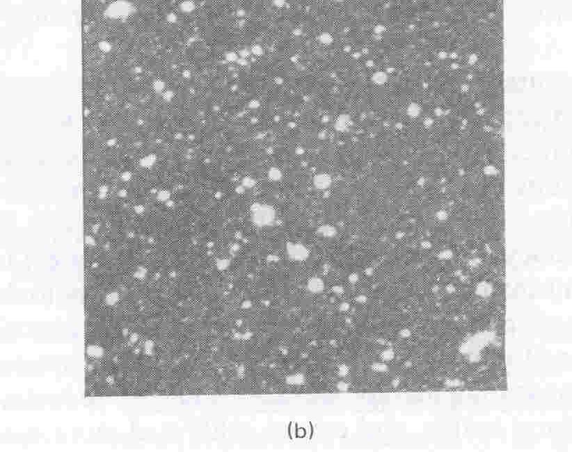
23 Electric potential Optical/IR Observational Astronomy Deep Depletion CCDs Ideally we require all the benefits of a thinned CCD plus an improved red response. The solution is to use a CCD with an intermediate thickness of about 40µm constructed from Hi-Resistivity silicon. The increased thickness makes the device opaque to red photons. The use of Hi-Resistivity silicon means that there are no field free regions despite the greater thickness. Cross section through a Deep Depletion CCD Problem : Hi resistivity silicon contains much lower impurity levels than normal. Very few wafer fabrication factories commonly use this material and deep depletion CCDs have to be designed and made to order. Red photons are now absorbed in the thicker bulk of the device. There is now a high electric field throughout the full depth of the CCD. CCDs manufactured in this way are known as Deep Depletion CCDs. The name implies that the region of high electric field, also known as the depletion zone extends deeply into the device. 23
24 CCD Detectors sensitivites II Quantum Efficiencies (QEs) are one of the most important parameters of a CCD. What are the properties of modern CCDs (e.g. buried channel, backilluminated, thinned, doped, deep-depletion, etc) 24
25 CCD Cameras Optical/IR Observational Astronomy CCD design has evolved considerably Better noise characteristics» R.N. of 2e now instead of 80e in 80s CCD controller is just as important as the CCD detector in terms of overall performance (e.g. noise) and versatility. This is what controls the clock voltages, i.e. readouts CCDs need cooling (reduce dark current ), i.e. thermal effects At 20ºC, a CCD can generate 100,000 ē/sec/pixel thermally Reducing T to 90 to 140ºC (i.e. 135 to 180K) reduces dark current to 10 s of ē/pixels per hour CCDs used in camera consisting of dewar, cryostat, pre-amp, signal proc. electronics, filters, etc. 25


26 Orthogonal transfer CCD (OTC) Optical/IR Observational Astronomy New developments in CCDs 4-phase CCD, but allowing charge shuffling both vertically and horizontally during exposure Half of CCD readout semi-continuously (storage half of frame-transfer type) Motion of a bright star in this half is used to clock the voltages on the OTC side Vertical transfers Horizontal transfers 26
27 New developments in CCDs Electron Multiplication CCDs (EMCCDs) Amplify signal in the serial readout register Avalanche gain Effectively a photon counting device Readout noise is insignificant Advantage for short exposures EMCCD Normal CCD 27
28 Drift-scanning with CCDs Clock charge along CCD rows at the same rate an object moves Good survey mode (e.g. Sloan Digital Sky Survey) 28
29 Add or combine charge packets at the output node capacitor On-Chip Binning These groupings become super-pixels Combined by either 1. delaying the serial register shift after a parallel shift, or 2. not resetting the output capacitor after a serial transfer 29
30 Readout Detectors Noise in IICCDs Ideally only associated with the output transistor (on-chip) Other noise sources arise from electronics affecting the weak signals (typically few 10 s of microvolts) Background charge associated with DC offsets Charge transfer fluctuations Reset ( ktc ) noise (resetting node output capacitance). Can be eliminated (e.g. correlated double sampling) MOSFET noise (transistor) Originally CCDs had readout noises of ~80ē Modern CCDs have 1 or 2ē readout noise Readout noise is constant signal added every time a CCD is readout Not proportional to the exposure time 30

.")
31 Bias Detectors and Overscan II Purposely bias the CCD video signal, so that readout noise never drives A/D input into the negative. Essentially it is a pedestal or DC offset signal which is ideally uniform and constant. Typical bias frame Modern CCDs have good bias (i.e. both constant in time and position). So rather than take bias frames (wasting time), just use part of the unilluminated portion of CCD (overscan). 31
 produced from")


32 Detectors Fringing II Interference pattern (e.g. Newton s rings) produced from night-sky emission lines (I.e. monochromatic sources) Particularly prevalent in thinned CCDs and at longer wavelengths Potentially highly variable (in position and time) up to 20%! 32


33 Removal of Fringing Before removal After removal 33

 Shape non-star like Easily removeable in software (replace with mean")
34 Cosmic Detectors Rays II CCDs are efficient at detecting the secondary particles of cosmic rays. These are typical muons which are absorbed in the Si lattice of the CCD Energy released from pair production leads to ~80ē/pixel/µm For a typical 20µm depth, a cosmic ray can generate ~1000ē Appears as a spike well above the background (many sigma of mean pixel values) Shape non-star like Easily removeable in software (replace with mean of surrounding pixels) 34
35 Optical elements in the light path (e.g. filters, windows) can accumulate small dust spot These are imaged as out-offocus spots ( doughnuts ) Generally stable over timescale of a night (unless in a dust storm) Will appear on every CCD frame Remove using flat field techniques Optical/IR Observational Astronomy Dust & dirt (!) 35


36 Flat Detectors Fielding II The excellent linear response of CCDs permits the technique of flat fielding. c = µ i i s Where: fi µ s is the mean pixel value of a n n sub-array of the flat field CCD frame r i is the value of the i th pixel in the raw CCD frame f i is the value of the i th pixel in the flat field CCD frame c i is the value of the i th pixel in the corrected CCD frame r 36
37 Signal-to-Noise A fundamental measurement with a CCD is the signal-to-noise ratio (S/N or SNR) Background signal (e.g. from sky ) can be subtracted from total (i.e. source + background) signal, even if the actual value of the background is >> source. What is important in defining how faint a source is detectable is the fluctuations of background (analogous to detecting a weak radio signal on a transistor radio in the presence of strong static). Noise processes are a result of independent events (i.e. photon arrivals) occurring at a (nearly) constant rate, described by Poisson statistics.» Standard deviation (rms of the fluctuations) is given by the simple formula: σ = (S t) 1/2, where S is the intensity (e.g. ē/sec) and t is the time interval 37
.")
38 Signal-to-Noise Poisson distribution implies that the errors inherent in a measurement have a Gaussian distribution. A S/N of unity is also called a 1-σ detection, and implies that there is a probability of 0.68 that the detection was real rather than a random fluke (i.e. 68% confidence). A S/N = 3 ( 3-σ detection) has a probability of being real (often used as a criterion for believing a result). Taking into account common noise sources and assuming Poisson statistics, the S/N ratio for a source of intensity S (photoelectrons/sec), observed for a time, t, whose photons fall into n pix pixels on the CCD detector, can be expressed as: Where B is the number of photoelectrons received from the background (per pixel per second), R n is the readout noise of the CCD, I d is the dark current of the detector, expressed in # of ē s/pixel/sec) and var( ) is the variance of the estimate of the total background, B t = (B + I d )t+ R n (again, per pixel per sec). The latter reflects uncertainty in estimating the background which does not arise from photon stats (i.e. from true variations in background level and inadequacies in the method of estimation). 38
39 Signal-to-Noise Usually the total background is estimated over many pixels (>> just source pixels) and sometimes over longer time interval (e.g. when the source is uniform, and little changing sky background) var(b t n pix t) term is often negligible Depending on the relative importance of various terms in the S/N equation, can define three main regimes: 1. Source photon-noise limited When source is bright and its photon noise dominates all other fluctuation S/N = (S t) 2. Detector-noise limited When both source and background are faint, and detector noise dominates S/N = S t / (I d n pix t) + (R n2 n pix ) This is the case where usually S/N increases linearly with time (when read noise dominates dark current). Can t take this to the extreme, however, due to cosmic ray hits. Background limited Also called sky limited, when source is faint and signal is dominated by the sky (e.g. sky glow, zodiacal light, background emission from other sources) S/N = S t / (B n pix ) This is the case where all instrumental noise is minimized, and the only option for increasing S/N is to observe longer ( t 1/2 ), or with a larger telescope ( S D 2 ) or better image quality (reduce n pix ) or reduced background. 39
40 40
Properties of a Detector
 Properties of a Detector Quantum Efficiency fraction of photons detected wavelength and spatially dependent Dynamic Range difference between lowest and highest measurable flux Linearity detection rate
CCD Analogy BUCKETS (PIXELS) HORIZONTAL CONVEYOR BELT (SERIAL REGISTER) VERTICAL CONVEYOR BELTS (CCD COLUMNS) RAIN (PHOTONS)
 HORIZONTAL CONVEYOR BELT (SERIAL REGISTER) VERTICAL CONVEYOR BELTS (CCD COLUMNS) RAIN (PHOTONS)") CCD Analogy RAIN (PHOTONS) VERTICAL CONVEYOR BELTS (CCD COLUMNS) BUCKETS (PIXELS) HORIZONTAL CONVEYOR BELT (SERIAL REGISTER) MEASURING CYLINDER (OUTPUT AMPLIFIER) Exposure finished, buckets now contain
CCD Analogy RAIN (PHOTONS) VERTICAL CONVEYOR BELTS (CCD COLUMNS) BUCKETS (PIXELS) HORIZONTAL CONVEYOR BELT (SERIAL REGISTER) MEASURING CYLINDER (OUTPUT AMPLIFIER) Exposure finished, buckets now contain
CCDS. Lesson I. Wednesday, August 29, 12
 CCDS Lesson I CCD OPERATION The predecessor of the CCD was a device called the BUCKET BRIGADE DEVICE developed at the Phillips Research Labs The BBD was an analog delay line, made up of capacitors such
The Charge-Coupled Device. Many overheads courtesy of Simon Tulloch
 The Charge-Coupled Device Astronomy 1263 Many overheads courtesy of Simon Tulloch smt@ing.iac.es Jan 24, 2013 What does a CCD Look Like? The fine surface electrode structure of a thick CCD is clearly visible
Three Ways to Detect Light. We now establish terminology for photon detectors:
 Three Ways to Detect Light In photon detectors, the light interacts with the detector material to produce free charge carriers photon-by-photon. The resulting miniscule electrical currents are amplified
An Introduction to CCDs. The basic principles of CCD Imaging is explained.
 An Introduction to CCDs. The basic principles of CCD Imaging is explained. Morning Brain Teaser What is a CCD? Charge Coupled Devices (CCDs), invented in the 1970s as memory devices. They improved the
CCD Characteristics Lab
 CCD Characteristics Lab Observational Astronomy 6/6/07 1 Introduction In this laboratory exercise, you will be using the Hirsch Observatory s CCD camera, a Santa Barbara Instruments Group (SBIG) ST-8E.
Charged-Coupled Devices
 Charged-Coupled Devices Charged-Coupled Devices Useful texts: Handbook of CCD Astronomy Steve Howell- Chapters 2, 3, 4.4 Measuring the Universe George Rieke - 3.1-3.3, 3.6 CCDs CCDs were invented in 1969
Detectors for microscopy - CCDs, APDs and PMTs. Antonia Göhler. Nov 2014
 Detectors for microscopy - CCDs, APDs and PMTs Antonia Göhler Nov 2014 Detectors/Sensors in general are devices that detect events or changes in quantities (intensities) and provide a corresponding output,
Dynamic Range. Can I look at bright and faint things at the same time?
 Detector Basics The purpose of any detector is to record the light collected by the telescope. All detectors transform the incident radiation into a some other form to create a permanent record, such as
Where detectors are used in science & technology
 Lecture 9 Outline Role of detectors Photomultiplier tubes (photoemission) Modulation transfer function Photoconductive detector physics Detector architecture Where detectors are used in science & technology
Astronomy 341 Fall 2012 Observational Astronomy Haverford College. CCD Terminology
 CCD Terminology Read noise An unavoidable pixel-to-pixel fluctuation in the number of electrons per pixel that occurs during chip readout. Typical values for read noise are ~ 10 or fewer electrons per
Photons and solid state detection
 Photons and solid state detection Photons represent discrete packets ( quanta ) of optical energy Energy is hc/! (h: Planck s constant, c: speed of light,! : wavelength) For solid state detection, photons
Introduction to CCD camera
 Observational Astronomy 2011/2012 Introduction to CCD camera Charge Coupled Device (CCD) photo sensor coupled to shift register Jörg R. Hörandel Radboud University Nijmegen http://particle.astro.ru.nl/goto.html?astropract1-1112
VII. IR Arrays & Readout VIII.CCDs & Readout. This lecture course follows the textbook Detection of
 Detection of Light VII. IR Arrays & Readout VIII.CCDs & Readout This lecture course follows the textbook Detection of Light 4-3-2016 by George Rieke, Detection Cambridge of Light Bernhard Brandl University
Charged Coupled Device (CCD) S.Vidhya
 S.Vidhya") Charged Coupled Device (CCD) S.Vidhya 02.04.2016 Sensor Physical phenomenon Sensor Measurement Output A sensor is a device that measures a physical quantity and converts it into a signal which can be read
Charged Coupled Device (CCD) S.Vidhya 02.04.2016 Sensor Physical phenomenon Sensor Measurement Output A sensor is a device that measures a physical quantity and converts it into a signal which can be read
Lecture 18: Photodetectors
 Lecture 18: Photodetectors Contents 1 Introduction 1 2 Photodetector principle 2 3 Photoconductor 4 4 Photodiodes 6 4.1 Heterojunction photodiode.................... 8 4.2 Metal-semiconductor photodiode................
Charge Coupled Devices. C. A. Griffith, Class Notes, PTYS 521, 2016 Not for distribution.
 Charge Coupled Devices C. A. Griffith, Class Notes, PTYS 521, 2016 Not for distribution. 1 1. Introduction While telescopes are able to gather more light from a distance source than does the naked eye,
Based on lectures by Bernhard Brandl
 Astronomische Waarneemtechnieken (Astronomical Observing Techniques) Based on lectures by Bernhard Brandl Lecture 10: Detectors 2 1. CCD Operation 2. CCD Data Reduction 3. CMOS devices 4. IR Arrays 5.
Three Ways to Detect Light. Following: Lord Rosse image of M33 vs. Hubble image demonstrate how critical detector technology is.
 Three Ways to Detect Light In photon detectors, the light interacts with the detector material to produce free charge carriers photon-by-photon. The resulting miniscule electrical currents are amplified
Welcome to: LMBR Imaging Workshop. Imaging Fundamentals Mike Meade, Photometrics
 Welcome to: LMBR Imaging Workshop Imaging Fundamentals Mike Meade, Photometrics Introduction CCD Fundamentals Typical Cooled CCD Camera Configuration Shutter Optic Sealed Window DC Voltage Serial Clock
STA1600LN x Element Image Area CCD Image Sensor
 ST600LN 10560 x 10560 Element Image Area CCD Image Sensor FEATURES 10560 x 10560 Photosite Full Frame CCD Array 9 m x 9 m Pixel 95.04mm x 95.04mm Image Area 100% Fill Factor Readout Noise 2e- at 50kHz
An Introduction to Scientific Imaging C h a r g e - C o u p l e d D e v i c e s
 p a g e 2 S C I E N T I F I C I M A G I N G T E C H N O L O G I E S, I N C. Introduction to the CCD F u n d a m e n t a l s The CCD Imaging A r r a y An Introduction to Scientific Imaging C h a r g e -
CHARGE-COUPLED DEVICE (CCD)
") CHARGE-COUPLED DEVICE (CCD) Definition A charge-coupled device (CCD) is an analog shift register, enabling analog signals, usually light, manipulation - for example, conversion into a digital value that
CHARGE-COUPLED DEVICE (CCD) Definition A charge-coupled device (CCD) is an analog shift register, enabling analog signals, usually light, manipulation - for example, conversion into a digital value that
Low Light Level CCD Performance and Issues
 Low Light Level CCD Performance and Issues Nagaraja Bezawada UK Astronomy Technology Centre 04 July 2007 Overview of the Talk Introduction to L3CCD (EM CCD) ULTRASPEC Performance and Issues New L3 CCD
Overview. Charge-coupled Devices. MOS capacitor. Charge-coupled devices. Charge-coupled devices:
 Overview Charge-coupled Devices Charge-coupled devices: MOS capacitors Charge transfer Architectures Color Limitations 1 2 Charge-coupled devices MOS capacitor The most popular image recording technology
Silicon sensors for radiant signals. D.Sc. Mikko A. Juntunen
 Silicon sensors for radiant signals D.Sc. Mikko A. Juntunen 2017 01 16 Today s outline Introduction Basic physical principles PN junction revisited Applications Light Ionizing radiation X-Ray sensors in
CCD reductions techniques
 CCD reductions techniques Origin of noise Noise: whatever phenomena that increase the uncertainty or error of a signal Origin of noises: 1. Poisson fluctuation in counting photons (shot noise) 2. Pixel-pixel
IV DETECTORS. Daguerrotype of the Moon, John W. Draper. March 26, 1840 New York
 IV DETECTORS Lit.: C.R.Kitchin: Astrophysical Techniques, 2009 C.D.Mckay: CCD s in Astronomy, Ann.Rev. A.&A. 24, 1986 G.H.Rieke: Infrared Detector Arrays for Astronomy, Ann.Rev. A&A 45, 2007 up to 1837:
Light gathering Power: Magnification with eyepiece:
 Telescopes Light gathering Power: The amount of light that can be gathered by a telescope in a given amount of time: t 1 /t 2 = (D 2 /D 1 ) 2 The larger the diameter the smaller the amount of time. If
What an Observational Astronomer needs to know!
 What an Observational Astronomer needs to know! IRAF:Photometry D. Hatzidimitriou Masters course on Methods of Observations and Analysis in Astronomy Basic concepts Counts how are they related to the actual
the need for an intensifier
 * The LLLCCD : Low Light Imaging without the need for an intensifier Paul Jerram, Peter Pool, Ray Bell, David Burt, Steve Bowring, Simon Spencer, Mike Hazelwood, Ian Moody, Neil Catlett, Philip Heyes Marconi
How Does One Obtain Spectral/Imaging Information! "
 How Does One Obtain Spectral/Imaging Information! How do we measure the position, energy, and arrival time of! an X-ray photon?! " What we observe depends on the instruments that one observes with!" In
Fundamentals of CMOS Image Sensors
 CHAPTER 2 Fundamentals of CMOS Image Sensors Mixed-Signal IC Design for Image Sensor 2-1 Outline Photoelectric Effect Photodetectors CMOS Image Sensor(CIS) Array Architecture CIS Peripherals Design Considerations
Introduction. Chapter 1
 1 Chapter 1 Introduction During the last decade, imaging with semiconductor devices has been continuously replacing conventional photography in many areas. Among all the image sensors, the charge-coupled-device
Chapter 3: Sensing the light: Detectors for the Optical and Infrared
 Chapter 3: Sensing the light: Detectors for the Optical and Infrared 3.1 Basic Properties of Photo-detectors Modern photon detectors operate by placing a bias voltage across a semiconductor crystal, illuminating
Ground-based optical auroral measurements
 Ground-based optical auroral measurements FYS 3610 Background Ground-based optical measurements provides a unique way to monitor spatial and temporal variation of auroral activity at high resolution up
Fully depleted, thick, monolithic CMOS pixels with high quantum efficiency
 Fully depleted, thick, monolithic CMOS pixels with high quantum efficiency Andrew Clarke a*, Konstantin Stefanov a, Nicholas Johnston a and Andrew Holland a a Centre for Electronic Imaging, The Open University,
Part I. CCD Image Sensors
 Part I CCD Image Sensors 2 Overview of CCD CCD is the abbreviation for charge-coupled device. CCD image sensors are silicon-based integrated circuits (ICs), consisting of a dense matrix of photodiodes
Page 1. Ground-based optical auroral measurements. Background. CCD All-sky Camera with filterwheel. Image intensifier
 Ground-based optical auroral measurements FYS 3610 Background Ground-based optical measurements provides a unique way to monitor spatial and temporal variation of auroral activity at high resolution up
Detectors. RIT Course Number Lecture Noise
 Detectors RIT Course Number 1051-465 Lecture Noise 1 Aims for this lecture learn to calculate signal-to-noise ratio describe processes that add noise to a detector signal give examples of how to combat
INTRODUCTION TO CCD IMAGING
 ASTR 1030 Astronomy Lab 85 Intro to CCD Imaging INTRODUCTION TO CCD IMAGING SYNOPSIS: In this lab we will learn about some of the advantages of CCD cameras for use in astronomy and how to process an image.
Lecture 2. Part 2 (Semiconductor detectors =sensors + electronics) Segmented detectors with pn-junction. Strip/pixel detectors
 Segmented detectors with pn-junction. Strip/pixel detectors") Lecture 2 Part 1 (Electronics) Signal formation Readout electronics Noise Part 2 (Semiconductor detectors =sensors + electronics) Segmented detectors with pn-junction Strip/pixel detectors Drift detectors
Lecture 2 Part 1 (Electronics) Signal formation Readout electronics Noise Part 2 (Semiconductor detectors =sensors + electronics) Segmented detectors with pn-junction Strip/pixel detectors Drift detectors
Charge-Coupled Device (CCD) Detectors pixel silicon chip electronics cryogenics
 Detectors pixel silicon chip electronics cryogenics") Charge-Coupled Device (CCD) Detectors As revolutionary in astronomy as the invention of the telescope and photography semiconductor detectors a collection of miniature photodiodes, each called a picture
Charge-Coupled Device (CCD) Detectors As revolutionary in astronomy as the invention of the telescope and photography semiconductor detectors a collection of miniature photodiodes, each called a picture
THE CCD RIDDLE REVISTED: SIGNAL VERSUS TIME LINEAR SIGNAL VERSUS VARIANCE NON-LINEAR
 THE CCD RIDDLE REVISTED: SIGNAL VERSUS TIME LINEAR SIGNAL VERSUS VARIANCE NON-LINEAR Mark Downing 1, Peter Sinclaire 1. 1 ESO, Karl Schwartzschild Strasse-2, 85748 Munich, Germany. ABSTRACT The photon
PHYS 3050 Electronics I
 PHYS 3050 Electronics I Chapter 4. Semiconductor Diodes and Transistors Earth, Moon, Mars, and Beyond Dr. Jinjun Shan, Associate Professor of Space Engineering Department of Earth and Space Science and
Components of Optical Instruments
 Components of Optical Instruments General Design of Optical Instruments Sources of Radiation Wavelength Selectors (Filters, Monochromators, Interferometers) Sample Containers Radiation Transducers (Detectors)
Electronic devices-i. Difference between conductors, insulators and semiconductors
 Electronic devices-i Semiconductor Devices is one of the important and easy units in class XII CBSE Physics syllabus. It is easy to understand and learn. Generally the questions asked are simple. The unit
Camera Test Protocol. Introduction TABLE OF CONTENTS. Camera Test Protocol Technical Note Technical Note
 Technical Note CMOS, EMCCD AND CCD CAMERAS FOR LIFE SCIENCES Camera Test Protocol Introduction The detector is one of the most important components of any microscope system. Accurate detector readings
STA3600A 2064 x 2064 Element Image Area CCD Image Sensor
 ST600A 2064 x 2064 Element Image Area CCD Image Sensor FEATURES 2064 x 2064 CCD Image Array 15 m x 15 m Pixel 30.96 mm x 30.96 mm Image Area Near 100% Fill Factor Readout Noise Less Than 3 Electrons at
a simple optical imager
 Imagers and Imaging a simple optical imager Here s one on our 61-Inch Telescope Here s one on our 61-Inch Telescope filter wheel in here dewar preamplifier However, to get a large field we cannot afford
FEATURES GENERAL DESCRIPTION. CCD Element Linear Image Sensor CCD Element Linear Image Sensor
 CCD 191 6000 Element Linear Image Sensor FEATURES 6000 x 1 photosite array 10µm x 10µm photosites on 10µm pitch Anti-blooming and integration control Enhanced spectral response (particularly in the blue
Simulation of High Resistivity (CMOS) Pixels
 Pixels") Simulation of High Resistivity (CMOS) Pixels Stefan Lauxtermann, Kadri Vural Sensor Creations Inc. AIDA-2020 CMOS Simulation Workshop May 13 th 2016 OUTLINE 1. Definition of High Resistivity Pixel Also
Simulation of High Resistivity (CMOS) Pixels Stefan Lauxtermann, Kadri Vural Sensor Creations Inc. AIDA-2020 CMOS Simulation Workshop May 13 th 2016 OUTLINE 1. Definition of High Resistivity Pixel Also
Semiconductor Detector Systems
 Semiconductor Detector Systems Helmuth Spieler Physics Division, Lawrence Berkeley National Laboratory OXFORD UNIVERSITY PRESS ix CONTENTS 1 Detector systems overview 1 1.1 Sensor 2 1.2 Preamplifier 3
Lecture 8 Optical Sensing. ECE 5900/6900 Fundamentals of Sensor Design
 ECE 5900/6900: Fundamentals of Sensor Design Lecture 8 Optical Sensing 1 Optical Sensing Q: What are we measuring? A: Electromagnetic radiation labeled as Ultraviolet (UV), visible, or near,mid-, far-infrared
 Electronic Devices 1. Current flowing in each of the following circuits A and respectively are: (Circuit 1) (Circuit 2) 1) 1A, 2A 2) 2A, 1A 3) 4A, 2A 4) 2A, 4A 2. Among the following one statement is not
Introduction to CCDs. Thanks to Simon Tulloch
 Introduction to CCDs. Thanks to Simon Tulloch smt@ing.iac.es What is a CCD? Charge Coupled Devices (CCDs) were invented in the 1970s and originally found application as memory devices. Their light sensitive
LEDs, Photodetectors and Solar Cells
 LEDs, Photodetectors and Solar Cells Chapter 7 (Parker) ELEC 424 John Peeples Why the Interest in Photons? Answer: Momentum and Radiation High electrical current density destroys minute polysilicon and
Strip Detectors. Principal: Silicon strip detector. Ingrid--MariaGregor,SemiconductorsasParticleDetectors. metallization (Al) p +--strips
 p +--strips") Strip Detectors First detector devices using the lithographic capabilities of microelectronics First Silicon detectors -- > strip detectors Can be found in all high energy physics experiments of the last
Strip Detectors First detector devices using the lithographic capabilities of microelectronics First Silicon detectors -- > strip detectors Can be found in all high energy physics experiments of the last
CCD1600A Full Frame CCD Image Sensor x Element Image Area
 - 1 - General Description CCD1600A Full Frame CCD Image Sensor 10560 x 10560 Element Image Area General Description The CCD1600 is a 10560 x 10560 image element solid state Charge Coupled Device (CCD)
Two-phase full-frame CCD with double ITO gate structure for increased sensitivity
 Two-phase full-frame CCD with double ITO gate structure for increased sensitivity William Des Jardin, Steve Kosman, Neal Kurfiss, James Johnson, David Losee, Gloria Putnam *, Anthony Tanbakuchi (Eastman
Semiconductor Physics and Devices
 Metal-Semiconductor and Semiconductor Heterojunctions The Metal-Oxide-Semiconductor Field-Effect Transistor (MOSFET) is one of two major types of transistors. The MOSFET is used in digital circuit, because
Astronomical Detectors. Lecture 3 Astronomy & Astrophysics Fall 2011
 Astronomical Detectors Lecture 3 Astronomy & Astrophysics Fall 2011 Detector Requirements Record incident photons that have been captured by the telescope. Intensity, Phase, Frequency, Polarization Difficulty
Review Energy Bands Carrier Density & Mobility Carrier Transport Generation and Recombination
 Review Energy Bands Carrier Density & Mobility Carrier Transport Generation and Recombination Current Transport: Diffusion, Thermionic Emission & Tunneling For Diffusion current, the depletion layer is
Order Overlap. A single wavelength constructively interferes in several directions A given direction can receive multiple wavelengths.
 Order Overlap A single wavelength constructively interferes in several directions A given direction can receive multiple wavelengths. Spectral Calibration TripleSpec Users Guide Spectral Calibration TripleSpec
Intro to Electricity. Introduction to Transistors. Example Circuit Diagrams. Water Analogy
 Introduction to Transistors Transistors form the basic building blocks of all computer hardware. Invented by William Shockley, John Bardeen and Walter Brattain in 1947, replacing previous vaccuumtube technology
UNIT 3 Transistors JFET
 UNIT 3 Transistors JFET Mosfet Definition of BJT A bipolar junction transistor is a three terminal semiconductor device consisting of two p-n junctions which is able to amplify or magnify a signal. It
Chapter 3 OPTICAL SOURCES AND DETECTORS
 Chapter 3 OPTICAL SOURCES AND DETECTORS 3. Optical sources and Detectors 3.1 Introduction: The success of light wave communications and optical fiber sensors is due to the result of two technological breakthroughs.
The 0.84 m Telescope OAN/SPM - BC, Mexico
 The 0.84 m Telescope OAN/SPM - BC, Mexico Readout error CCD zero-level (bias) ramping CCD bias frame banding Shutter failure Significant dark current Image malting Focus frame taken during twilight IR
Control of Noise and Background in Scientific CMOS Technology
 Control of Noise and Background in Scientific CMOS Technology Introduction Scientific CMOS (Complementary metal oxide semiconductor) camera technology has enabled advancement in many areas of microscopy
OPTOELECTRONIC and PHOTOVOLTAIC DEVICES
 OPTOELECTRONIC and PHOTOVOLTAIC DEVICES Outline 1. Introduction to the (semiconductor) physics: energy bands, charge carriers, semiconductors, p-n junction, materials, etc. 2. Light emitting diodes Light
Observing*Checklist:*A3ernoon*
 Ay#122a:# Intro#to#Observing/Image#Processing# (Many&slides&today& c/o&m.&bolte)& Observing*Checklist:*A3ernoon* Set*up*instrument*(verify*and*set*filters,*gra@ngs,*etc.)* Set*up*detector*(format,*gain,*binning)*
Engineering Medical Optics BME136/251 Winter 2018
 Engineering Medical Optics BME136/251 Winter 2018 Monday/Wednesday 2:00-3:20 p.m. Beckman Laser Institute Library, MSTB 214 (lab) *1/17 UPDATE Wednesday, 1/17 Optics and Photonic Devices III: homework
Amplifier Luminescence and RBI. Richard Crisp May 21,
 Amplifier Luminescence and RBI Richard Crisp May 21, 2013 rdcrisp@earthlink.net www.narrowbandimaging.com Outline What is amplifier luminescence? What mechanism causes amplifier luminescence at the transistor
FIBER OPTICS. Prof. R.K. Shevgaonkar. Department of Electrical Engineering. Indian Institute of Technology, Bombay. Lecture: 20
 FIBER OPTICS Prof. R.K. Shevgaonkar Department of Electrical Engineering Indian Institute of Technology, Bombay Lecture: 20 Photo-Detectors and Detector Noise Fiber Optics, Prof. R.K. Shevgaonkar, Dept.
Difference between BJTs and FETs. Junction Field Effect Transistors (JFET)
") Difference between BJTs and FETs Transistors can be categorized according to their structure, and two of the more commonly known transistor structures, are the BJT and FET. The comparison between BJTs
Difference between BJTs and FETs Transistors can be categorized according to their structure, and two of the more commonly known transistor structures, are the BJT and FET. The comparison between BJTs
Astronomy /6/15. In this Lecture: (Detector Technology) Nomenclature. Lecture 3: Introduction to CCD and CMOS Imaging Devices
 Nomenclature. Lecture 3: Introduction to CCD and CMOS Imaging Devices") Astronomy 3310 Lecture 3: Introduction to CCD and CMOS Imaging Devices Lecture 3 Astro 3310 1 In this Lecture: (Detector Technology) Introduc/on to Solid State Detectors CCD CMOS and IRFPA Basic CCD /
Astronomy 3310 Lecture 3: Introduction to CCD and CMOS Imaging Devices Lecture 3 Astro 3310 1 In this Lecture: (Detector Technology) Introduc/on to Solid State Detectors CCD CMOS and IRFPA Basic CCD /
Detailed Characterisation of a New Large Area CCD Manufactured on High Resistivity Silicon
 Detailed Characterisation of a New Large Area CCD Manufactured on High Resistivity Silicon Mark S. Robbins *, Pritesh Mistry, Paul R. Jorden e2v technologies Ltd, 106 Waterhouse Lane, Chelmsford, Essex
Low noise readout techniques for Charge Coupled Devices (CCD) Gustavo Cancelo, Juan Estrada, Guillermo Fernandez Moroni, Ken Treptow, Ted Zmuda
 Gustavo Cancelo, Juan Estrada, Guillermo Fernandez Moroni, Ken Treptow, Ted Zmuda") Low noise readout techniques for Charge Coupled Devices (CCD) Gustavo Cancelo, Juan Estrada, Guillermo Fernandez Moroni, Ken Treptow, Ted Zmuda Charge Coupled Devices (CCD) Potential well Characteristics:
Low noise readout techniques for Charge Coupled Devices (CCD) Gustavo Cancelo, Juan Estrada, Guillermo Fernandez Moroni, Ken Treptow, Ted Zmuda Charge Coupled Devices (CCD) Potential well Characteristics:
Optical Amplifiers. Continued. Photonic Network By Dr. M H Zaidi
 Optical Amplifiers Continued EDFA Multi Stage Designs 1st Active Stage Co-pumped 2nd Active Stage Counter-pumped Input Signal Er 3+ Doped Fiber Er 3+ Doped Fiber Output Signal Optical Isolator Optical
CCD30-11 NIMO Back Illuminated Deep Depleted High Performance CCD Sensor
 CCD30-11 NIMO Back Illuminated Deep Depleted High Performance CCD Sensor FEATURES 1024 by 256 Pixel Format 26µm Square Pixels Image area 26.6 x 6.7mm Back Illuminated format for high quantum efficiency
Abstract. Preface. Acknowledgments
 Contents Abstract Preface Acknowledgments iv v vii 1 Introduction 1 1.1 A Very Brief History of Visible Detectors in Astronomy................ 1 1.2 The CCD: Astronomy s Champion Workhorse......................
Downloaded from
 SOLID AND SEMICONDUCTOR DEVICES (EASY AND SCORING TOPIC) 1. Distinction of metals, semiconductor and insulator on the basis of Energy band of Solids. 2. Types of Semiconductor. 3. PN Junction formation
3/27/17. Detector Basics. Quantum Efficiency (QE) and Spectral Response. Quantum Efficiency (QE) and Spectral Response
 and Spectral Response. Quantum Efficiency (QE) and Spectral Response") 3/27/17 Detector Basics The purpose of any detector is to record the light collected by the telescope. All detectors transform the incident radiation into a some other form to create a permanent record,
3/27/17 Detector Basics The purpose of any detector is to record the light collected by the telescope. All detectors transform the incident radiation into a some other form to create a permanent record,
IT FR R TDI CCD Image Sensor
 4k x 4k CCD sensor 4150 User manual v1.0 dtd. August 31, 2015 IT FR 08192 00 R TDI CCD Image Sensor Description: With the IT FR 08192 00 R sensor ANDANTA GmbH builds on and expands its line of proprietary
Charge coupled CMOS and hybrid detector arrays
 Charge coupled CMOS and hybrid detector arrays James Janesick Sarnoff Corporation, 4952 Warner Ave., Suite 300, Huntington Beach, CA. 92649 Headquarters: CN5300, 201 Washington Road Princeton, NJ 08543-5300
CCD47-10 NIMO Back Illuminated Compact Pack High Performance CCD Sensor
 CCD47-10 NIMO Back Illuminated Compact Pack High Performance CCD Sensor FEATURES 1024 by 1024 Nominal (1056 by 1027 Usable Pixels) Image area 13.3 x 13.3mm Back Illuminated format for high quantum efficiency
3/5/17. Detector Basics. Quantum Efficiency (QE) and Spectral Response. Quantum Efficiency (QE) and Spectral Response
 and Spectral Response. Quantum Efficiency (QE) and Spectral Response") 3/5/17 Detector Basics The purpose of any detector is to record the light collected by the telescope. All detectors transform the incident radiation into a some other form to create a permanent record,
3/5/17 Detector Basics The purpose of any detector is to record the light collected by the telescope. All detectors transform the incident radiation into a some other form to create a permanent record,
Astro-photography. Daguerreotype: on a copper plate
 AST 1022L Astro-photography 1840-1980s: Photographic plates were astronomers' main imaging tool At right: first ever picture of the full moon, by John William Draper (1840) Daguerreotype: exposure using
Chapter Semiconductor Electronics
 Chapter Semiconductor Electronics Q1. p-n junction is said to be forward biased, when [1988] (a) the positive pole of the battery is joined to the p- semiconductor and negative pole to the n- semiconductor
J. Janesick, S.A. Collins, and E.R. Fossum Imaging Systems Section Jet Propulsion Laboratory Pasadena, CA 91109
 Scientific CCD Technology at JPL J. Janesick, S.A. Collins, and E.R. Fossum maging Systems Section Jet Propulsion Laboratory Pasadena, CA 91109 ntroduction Charge-coupled devices (CCOs) were recognized
 Energy band diagrams Metals: 9. ELECTRONIC DEVICES GIST ρ= 10-2 to 10-8 Ω m Insulators: ρ> 10 8 Ω m Semiconductors ρ= 1 to 10 5 Ω m 109 A. Intrinsic semiconductors At T=0k it acts as insulator At room
Unit 2 Semiconductor Devices. Lecture_2.5 Opto-Electronic Devices
 Unit 2 Semiconductor Devices Lecture_2.5 Opto-Electronic Devices Opto-electronics Opto-electronics is the study and application of electronic devices that interact with light. Electronics (electrons) Optics
CMOS Detectors Ingeniously Simple!
 CMOS Detectors Ingeniously Simple! A.Schöning University Heidelberg B-Workshop Neckarzimmern 18.-20.2.2015 1 Detector System on Chip? 2 ATLAS Pixel Module 3 ATLAS Pixel Module MCC sensor FE-Chip FE-Chip
CONTENTS. 2.2 Schrodinger's Wave Equation 31. PART I Semiconductor Material Properties. 2.3 Applications of Schrodinger's Wave Equation 34
 CONTENTS Preface x Prologue Semiconductors and the Integrated Circuit xvii PART I Semiconductor Material Properties CHAPTER 1 The Crystal Structure of Solids 1 1.0 Preview 1 1.1 Semiconductor Materials
THERMIONIC AND GASEOUS STATE DIODES
 THERMIONIC AND GASEOUS STATE DIODES Thermionic and gaseous state (vacuum tube) diodes Thermionic diodes are thermionic-valve devices (also known as vacuum tubes, tubes, or valves), which are arrangements
Resonant Tunneling Device. Kalpesh Raval
 Resonant Tunneling Device Kalpesh Raval Outline Diode basics History of Tunnel diode RTD Characteristics & Operation Tunneling Requirements Various Heterostructures Fabrication Technique Challenges Application
UNIT-VI FIELD EFFECT TRANSISTOR. 1. Explain about the Field Effect Transistor and also mention types of FET s.
 UNIT-I FIELD EFFECT TRANSISTOR 1. Explain about the Field Effect Transistor and also mention types of FET s. The Field Effect Transistor, or simply FET however, uses the voltage that is applied to their
Optical Receivers Theory and Operation
 Optical Receivers Theory and Operation Photo Detectors Optical receivers convert optical signal (light) to electrical signal (current/voltage) Hence referred O/E Converter Photodetector is the fundamental
Design and Performance of a Pinned Photodiode CMOS Image Sensor Using Reverse Substrate Bias
 Design and Performance of a Pinned Photodiode CMOS Image Sensor Using Reverse Substrate Bias 13 September 2017 Konstantin Stefanov Contents Background Goals and objectives Overview of the work carried