LEDs, Photodetectors and Solar Cells
|
|
|
- Melvin Daniel
- 5 years ago
- Views:
Transcription
1 LEDs, Photodetectors and Solar Cells Chapter 7 (Parker) ELEC 424 John Peeples
2 Why the Interest in Photons? Answer: Momentum and Radiation High electrical current density destroys minute polysilicon and metal traces on ICs. Joule heating leads to fusing Electromigration Photons have very low momentum. Electrical particles radiate energy as the 4 th power of their frequency. The source of crosstalk High frequency photons are much less prone to crosstalk. Thus our interest in: LEDs and Lasers as that emit photons in response to electrical input Solar Cells and Photodetectors that emit electricity in response to photonic input
3 Light Emitting Diodes Essentially a diode made from direct band-gap or modified indirect band-gap material. Injection electroluminescence Carriers are injected Electron and hole recombination results in luminescence Photon energy is that of the band-gap of the material. A forward biased diode injects many electrons into the p-side and holes into the n-side where than can recombine and emit a photon if made from the proper material.
4 LEDs Electron diffusion lengths are typically longer Than that of holes, so the majority of the photon emission will be on the p-side Favorite structure is n ++ -p Band-gap determines photon energy and therefore also determines photon frequency. The E-M spectrum covers about ev Gamma rays at ~10 9 ev The weakest photons at about ev Our eyes detect between 2 and 3 ev! Specific Colors require specific semiconductor materials.
 can cover the range, but comes in n-type and does not like to be doped to p-type In the real world, no single alloyed system can span")
5 LED Materials We want devices to emit from infrared to ultraviolet. GaN 2 ev InGaN 3.3 ev The InGaN system (InN, GaN, AlN, InGaN, AlGaN and InAlGaN) can cover the range, but comes in n-type and does not like to be doped to p-type In the real world, no single alloyed system can span the visible light range. Gallium Arsenide System for Reds GaAs 1.43 ev infrared Add Al to increase the band-gap Ga.56 Al.44 As 1.96 ev Red Heterojunctions for Brightness
 Grown on the InP (Indium Phosphide) crystal Longer Wavelengths (5 μm to 50 μm) PbSnTe (Lead Tin Telluride) PbSnSe (Lead Tin Selenide) Visible")
6 Other LED Materials Fiber Optics have absorption minima at 1.3 and 1.55μm wavelengths. Alloys of GaInAsP (Gallium Indium Arsenide Phosphide) Grown on the InP (Indium Phosphide) crystal Longer Wavelengths (5 μm to 50 μm) PbSnTe (Lead Tin Telluride) PbSnSe (Lead Tin Selenide) Visible Light Reds Gallium Arsenide Phosphide The GaAs 1-x P x is an indirect semiconductor at x > 0.45 Employs Isoelectronic Centers to produce red, yellow, amber and green LEDs
7 Isoelectronic Centers An isoelectronic center is a crystal lattice site at which the atom has been replaced by another of the same valence electron structure. Consider Nitrogen replacing Phosphorous in GaP The center is not a dopant atom It has the same electron structure. Heisenberg The center s location is known It is at a lattice site It must have a wide momentum band The center is a stepping stone to efficient recombination with no momentum change
8 An LED for All Seasons Red Gallium Arsenide Phosphide (direct semiconduction) Orange, Yellow and Green Blue Gallium Arsenide Phosphide Nitride (isoelectronic centers) Silicon Carbide with N and Al doping (indirect, impurity centers) Gallium Nitride with Zn doping (indirect, impurity centers) (Best) Direct Band-to-Band Recombination Recombination via isoelectronic centers Recombination via impurity centers (Worst) Indirect Band-to-Band recombination
 What is the electrical to optical efficiency of each? E ev = 1.")
9 Example For the LEDs above a) What is the band-gap for each? b) At 30% radiative recombination efficiency, what optical power is emitted by each? c) What is the input power to each? d) What is the electrical to optical efficiency of each? E ev = 1.24 wavelength (μm) and the optical power will be the radiative efficiency time the diode current time the band-gap (photon) energy.

10 Junction Photodetectors (Photodiodes) LEDs source light and Photodetectors sense light. Life is great. Photodetectors need not be direct-gap semiconductors. They must have the right band-gap energy. Photons create hole-electron pairs if their energy is greater than the band-gap. E ev = 1.24 wavelength (μm) A PN junction and a little anti reflection Coating and you have a photodetector.
11 Cut-off Wavelength Photon energy must be greater than the material bandgap. E ev 1.24 = wavelength (μm) So for Silicon, the cut-off wavelength must be infrared or slightly shorter (red). But not too short! The photon intensity at distance x into the silicon is an exponential function, I = I 0 e ax where I 0 = incident photon intensity in watts per unit area. Short wavelength photons have large absorption coefficients. Electron-hole pairs generated within or at the edge of the depletion region will be separated by the electric field at nearly the saturation drift velocity 10 7 cm/s for silicon. Once separated they enter into the n- or p- regions as majority carriers and become current in the external circuit.
12 What Makes a Good Photodetector? A wide depletion region Reverse bias Low absorption Highly doped thin top junction Lowly doped bottom junction Low junction capacitance See both above The only trade off is the increased transit time across the wide depletion region.
13 Photodiode Example A HeNe laser puts out nm light, modulated at 6 GHz. What will the silicon photodiode depletion width be that provides a transit time of onehalf the modulation frequency period? 1/(3x10 9 Hz) = 3.33x10 10 s Remembering that the saturation drift velocity in silicon is about 10 7 cm/s the depletion region width will be 3.33x10 10 x 10 7 = 33.3μm
14 Photodiode Final Thoughts Tailoring the depletion region width is critical because we are often stuck with the incoming photon wavelengths and the photodiode material. Reverse bias and doping are one way, P-I-N (P-Intrinsic-N) structures are another. A lowly doped intrinsic region separate thin p + and n + regions. Virtually all the reverse bias drops across the I region, ensuring rapid carrier sweep-out. Quantum efficiency and frequency response are optimized in this case, but the width of the I region.
15 Photoconductor Not a junction diode. Just a slab of semiconductor material with metal terminals. Can be intrinsic or extrinsic. Chapter 4 doping/resistivity analysis applies. Can yield more electron/hole current carriers than incoming photons (positive gain)!
16 Photoconductor Cell thickness, D, must be a little greater than 1/α. Intrinsic, N-type and P-type charge carrier generation. Intrinsic requires incoming photon with energy greater than the bandgap. N- and P- type photon energies are clearly less than half the band-gap.
17 Photodetector Gain Gedanken Consider a small extrinsic photodetector with only one donor atom sitting unionized at a single donor site. The small photodetector is at very low temperature and has no applied electric field. No current flows until a single photon arrives and ionizes the one donor atom. The fact that the donor electron leaves the device and is replaced by a second electron as shown in case (b) on the prior slide, represents current gain but only for a time until the donor center recaptures the conduction band electron. This gain can be quantized as the carrier lifetime over the time taken by the electron to transit the detector (carrier transit time). Gain = τ t tr Unfortunately if you want a fast device, you employ lifetime killers and therefore limit gain. Fast response means low sensitivity. Everything is a trade-off.
18 Solar Cell A photodetector provided an electrical current when reverse biased but we really don t need any bias. Illuminating a silicon PN junction with full spectrum visible light instigates charge separation in and close to the depletion region. Assumes light energy larger than the band-gap There will be a terminal voltage at zero current, V oc. This light-generated V oc is called the photovoltaic effect.
19 Open Circuit Voltage To find the magnitude of V oc, we solve the ideal diode equation, I = i 0 e qv kt 1 for V. V = kt q ln 1 + I I 0 In terms of photocurrent; V oc = kt q ln 1 + I p I 0 V oc < V bi < E g q V oc is typically less than one volt, and I sc is about 20 ma/cm 2 for silicon. Many cells in parallel provides V and large overall area to provides I.
20 Fill Factor Fill Factor = I mv m I sc V oc
21 The Bottom Line on Solar Cells Useful solar panels must have large surface area and include a number of cells in parallel in order to produce useful electrical output. This makes silicon a favored material. The Good: Sunlight has reasonable power content from 0.3 to 1.5 μm wavelength. The Bad: Silicon is transparent beyond 1 μm and not that good on the short wavelength end. This means we must work hard to absorb all incoming light. Surface area enhanced by pyramidal etching. Reflection damped by coatings. The Ugly: A single-value energy-gap responds only to a portion of the light spectrum. Multijunction structures have limited application and are typically compound semiconductor material. Impressive R & D has yielded impressive efficiencies.
22
Lecture 18: Photodetectors
 Lecture 18: Photodetectors Contents 1 Introduction 1 2 Photodetector principle 2 3 Photoconductor 4 4 Photodiodes 6 4.1 Heterojunction photodiode.................... 8 4.2 Metal-semiconductor photodiode................
Optical Amplifiers. Continued. Photonic Network By Dr. M H Zaidi
 Optical Amplifiers Continued EDFA Multi Stage Designs 1st Active Stage Co-pumped 2nd Active Stage Counter-pumped Input Signal Er 3+ Doped Fiber Er 3+ Doped Fiber Output Signal Optical Isolator Optical
OPTOELECTRONIC and PHOTOVOLTAIC DEVICES
 OPTOELECTRONIC and PHOTOVOLTAIC DEVICES Outline 1. Introduction to the (semiconductor) physics: energy bands, charge carriers, semiconductors, p-n junction, materials, etc. 2. Light emitting diodes Light
PHYSICAL ELECTRONICS(ECE3540) APPLICATIONS OF PHYSICAL ELECTRONICS PART I
 APPLICATIONS OF PHYSICAL ELECTRONICS PART I") PHYSICAL ELECTRONICS(ECE3540) APPLICATIONS OF PHYSICAL ELECTRONICS PART I Tennessee Technological University Monday, October 28, 2013 1 Introduction In the following slides, we will discuss the summary
PHYSICAL ELECTRONICS(ECE3540) APPLICATIONS OF PHYSICAL ELECTRONICS PART I Tennessee Technological University Monday, October 28, 2013 1 Introduction In the following slides, we will discuss the summary
CONTENTS. 2.2 Schrodinger's Wave Equation 31. PART I Semiconductor Material Properties. 2.3 Applications of Schrodinger's Wave Equation 34
 CONTENTS Preface x Prologue Semiconductors and the Integrated Circuit xvii PART I Semiconductor Material Properties CHAPTER 1 The Crystal Structure of Solids 1 1.0 Preview 1 1.1 Semiconductor Materials
Key Questions ECE 340 Lecture 28 : Photodiodes
 Things you should know when you leave Key Questions ECE 340 Lecture 28 : Photodiodes Class Outline: How do the I-V characteristics change with illumination? How do solar cells operate? How do photodiodes
Electronics The basics of semiconductor physics
 Electronics The basics of semiconductor physics Prof. Márta Rencz, Gábor Takács BME DED 17/09/2015 1 / 37 The basic properties of semiconductors Range of conductivity [Source: http://www.britannica.com]
ECE 340 Lecture 29 : LEDs and Lasers Class Outline:
 ECE 340 Lecture 29 : LEDs and Lasers Class Outline: Light Emitting Diodes Lasers Semiconductor Lasers Things you should know when you leave Key Questions What is an LED and how does it work? How does a
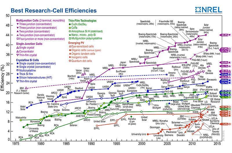
What is the highest efficiency Solar Cell?
 What is the highest efficiency Solar Cell? GT CRC Roof-Mounted PV System Largest single PV structure at the time of it s construction for the 1996 Olympic games Produced more than 1 billion watt hrs. of
Key Questions. What is an LED and how does it work? How does a laser work? How does a semiconductor laser work? ECE 340 Lecture 29 : LEDs and Lasers
 Things you should know when you leave Key Questions ECE 340 Lecture 29 : LEDs and Class Outline: What is an LED and how does it How does a laser How does a semiconductor laser How do light emitting diodes
LAB V. LIGHT EMITTING DIODES
 LAB V. LIGHT EMITTING DIODES 1. OBJECTIVE In this lab you are to measure I-V characteristics of Infrared (IR), Red and Blue light emitting diodes (LEDs). The emission intensity as a function of the diode
Università degli Studi di Roma Tor Vergata Dipartimento di Ingegneria Elettronica. Analogue Electronics. Paolo Colantonio A.A.
 Università degli Studi di Roma Tor Vergata Dipartimento di Ingegneria Elettronica Analogue Electronics Paolo Colantonio A.A. 2015-16 Introduction: materials Conductors e.g. copper or aluminum have a cloud
LAB V. LIGHT EMITTING DIODES
 LAB V. LIGHT EMITTING DIODES 1. OBJECTIVE In this lab you will measure the I-V characteristics of Infrared (IR), Red and Blue light emitting diodes (LEDs). Using a photodetector, the emission intensity
Chapter 3 OPTICAL SOURCES AND DETECTORS
 Chapter 3 OPTICAL SOURCES AND DETECTORS 3. Optical sources and Detectors 3.1 Introduction: The success of light wave communications and optical fiber sensors is due to the result of two technological breakthroughs.
Photodiode: LECTURE-5
 LECTURE-5 Photodiode: Photodiode consists of an intrinsic semiconductor sandwiched between two heavily doped p-type and n-type semiconductors as shown in Fig. 3.2.2. Sufficient reverse voltage is applied
Diodes Rectifiers, Zener diodes light emitting diodes, laser diodes photodiodes, optocouplers
 Diodes Rectifiers, Zener diodes light emitting diodes, laser diodes photodiodes, optocouplers Prepared by Scott Robertson Fall 2007 Physics 3330 1 Impurity-doped semiconductors Semiconductors (Ge, Si)
Downloaded from
 SOLID AND SEMICONDUCTOR DEVICES (EASY AND SCORING TOPIC) 1. Distinction of metals, semiconductor and insulator on the basis of Energy band of Solids. 2. Types of Semiconductor. 3. PN Junction formation
Functional Materials. Optoelectronic devices
 Functional Materials Lecture 2: Optoelectronic materials and devices (inorganic). Photonic materials Optoelectronic devices Light-emitting diode (LED) displays Photodiode and Solar cell Photoconductive
Optical Receivers Theory and Operation
 Optical Receivers Theory and Operation Photo Detectors Optical receivers convert optical signal (light) to electrical signal (current/voltage) Hence referred O/E Converter Photodetector is the fundamental
Luminous Equivalent of Radiation
 Intensity vs λ Luminous Equivalent of Radiation When the spectral power (p(λ) for GaP-ZnO diode has a peak at 0.69µm) is combined with the eye-sensitivity curve a peak response at 0.65µm is obtained with
10/14/2009. Semiconductor basics pn junction Solar cell operation Design of silicon solar cell
 PHOTOVOLTAICS Fundamentals PV FUNDAMENTALS Semiconductor basics pn junction Solar cell operation Design of silicon solar cell SEMICONDUCTOR BASICS Allowed energy bands Valence and conduction band Fermi
Semiconductor Lasers Semiconductors were originally pumped by lasers or e-beams First diode types developed in 1962: Create a pn junction in
 Semiconductor Lasers Semiconductors were originally pumped by lasers or e-beams First diode types developed in 1962: Create a pn junction in semiconductor material Pumped now with high current density
Electronic devices-i. Difference between conductors, insulators and semiconductors
 Electronic devices-i Semiconductor Devices is one of the important and easy units in class XII CBSE Physics syllabus. It is easy to understand and learn. Generally the questions asked are simple. The unit
LED lecture. Wei Chih Wang University of Washington
 LED lecture Wei Chih Wang University of Washington Linear and Nonlinear electronics current voltage Vaccum tube (i.e. type 2A3) voltage Thermistor (large negative temperature coefficient of resistivity)
Problem 4 Consider a GaAs p-n + junction LED with the following parameters at 300 K: Electron diusion coecient, D n = 25 cm 2 =s Hole diusion coecient
 Prof. Jasprit Singh Fall 2001 EECS 320 Homework 7 This homework is due on November 8. Problem 1 An optical power density of 1W/cm 2 is incident on a GaAs sample. The photon energy is 2.0 ev and there is
1 Semiconductor-Photon Interaction
 1 SEMICONDUCTOR-PHOTON INTERACTION 1 1 Semiconductor-Photon Interaction Absorption: photo-detectors, solar cells, radiation sensors. Radiative transitions: light emitting diodes, displays. Stimulated emission:
Solar Cell Parameters and Equivalent Circuit
 9 Solar Cell Parameters and Equivalent Circuit 9.1 External solar cell parameters The main parameters that are used to characterise the performance of solar cells are the peak power P max, the short-circuit
Intrinsic Semiconductor
 Semiconductors Crystalline solid materials whose resistivities are values between those of conductors and insulators. Good electrical characteristics and feasible fabrication technology are some reasons
Microelectronic Devices and Circuits Lecture 8 - BJTs Wrap-up, Solar Cells, LEDs - Outline
 6.012 - Microelectronic Devices and Circuits Lecture 8 - BJTs Wrap-up, Solar Cells, LEDs - Outline Announcements Exam One - Tomorrow, Wednesday, October 7, 7:30 pm BJT Review Wrapping up BJTs (for now)
Fall 2004 Dawn Hettelsater, Yan Zhang and Ali Shakouri, 05/09/2002
 University of California at Santa Cruz Jack Baskin School of Engineering Electrical Engineering Department EE-145L: Properties of Materials Laboratory Lab 6: Solar Cells Fall 2004 Dawn Hettelsater, Yan
Department of Electrical Engineering IIT Madras
 Department of Electrical Engineering IIT Madras Sample Questions on Semiconductor Devices EE3 applicants who are interested to pursue their research in microelectronics devices area (fabrication and/or
Semiconductor Lasers Semiconductors were originally pumped by lasers or e-beams First diode types developed in 1962: Create a pn junction in
 Semiconductor Lasers Semiconductors were originally pumped by lasers or e-beams First diode types developed in 1962: Create a pn junction in semiconductor material Pumped now with high current density
UNIT-III SOURCES AND DETECTORS. According to the shape of the band gap as a function of the momentum, semiconductors are classified as
 UNIT-III SOURCES AND DETECTORS DIRECT AND INDIRECT BAND GAP SEMICONDUCTORS: According to the shape of the band gap as a function of the momentum, semiconductors are classified as 1. Direct band gap semiconductors
10/27/2009 Reading: Chapter 10 of Hambley Basic Device Physics Handout (optional)
") EE40 Lec 17 PN Junctions Prof. Nathan Cheung 10/27/2009 Reading: Chapter 10 of Hambley Basic Device Physics Handout (optional) Slide 1 PN Junctions Semiconductor Physics of pn junctions (for reference
EE40 Lec 17 PN Junctions Prof. Nathan Cheung 10/27/2009 Reading: Chapter 10 of Hambley Basic Device Physics Handout (optional) Slide 1 PN Junctions Semiconductor Physics of pn junctions (for reference
Chap14. Photodiode Detectors
 Chap14. Photodiode Detectors Mohammad Ali Mansouri-Birjandi mansouri@ece.usb.ac.ir mamansouri@yahoo.com Faculty of Electrical and Computer Engineering University of Sistan and Baluchestan (USB) Design
EEE118: Electronic Devices and Circuits
 EEE118: Electronic Devices and Circuits Lecture IIII James E Green Department of Electronic Engineering University of Sheffield j.e.green@sheffield.ac.uk Last Lecture: Review 1 Defined some terminology
Optical Fiber Communication Lecture 11 Detectors
 Optical Fiber Communication Lecture 11 Detectors Warriors of the Net Detector Technologies MSM (Metal Semiconductor Metal) PIN Layer Structure Semiinsulating GaAs Contact InGaAsP p 5x10 18 Absorption InGaAs
Study and Measurement of the Main Parameters of a Laser quadrant Detector
 Cairo University National Institute of Laser Enhanced Sciences Laser Sciences and Interactions Study and Measurement of the Main Parameters of a Laser quadrant Detector By Eng. Mohamed Abd-Elfattah Abd-Elazim
UNIT IX ELECTRONIC DEVICES
 UNT X ELECTRONC DECES Weightage Marks : 07 Semiconductors Semiconductors diode-- characteristics in forward and reverse bias, diode as rectifier. - characteristics of LED, Photodiodes, solarcell and Zener
Physics and Technology
 Physics and Technology Emitters Materials Infrared emitting diodes (IREDs) can be produced from a range of different III-V compounds. Unlike the elemental semiconductor silicon, the compound III-V semiconductors
Optical Sources and Detectors
 Optical Sources and Detectors 1. Optical Sources Optical transmitter coverts electrical input signal into corresponding optical signal. The optical signal is then launched into the fiber. Optical source
Optodevice Data Book ODE I. Rev.9 Mar Opnext Japan, Inc.
 Optodevice Data Book ODE-408-001I Rev.9 Mar. 2003 Opnext Japan, Inc. Section 1 Operating Principles 1.1 Operating Principles of Laser Diodes (LDs) and Infrared Emitting Diodes (IREDs) 1.1.1 Emitting Principles
Light Sources, Modulation, Transmitters and Receivers
 Optical Fibres and Telecommunications Light Sources, Modulation, Transmitters and Receivers Introduction Previous section looked at Fibres. How is light generated in the first place? How is light modulated?
PN Junction Diode Table of Contents. What Are Diodes Made Out Of?
 PN Junction iode Table of Contents What are diodes made out of?slide 3 N-type materialslide 4 P-type materialslide 5 The pn junctionslides 6-7 The biased pn junctionslides 8-9 Properties of diodesslides
Fundamentals of Laser
 SMR 1826-3 Preparatory School to the Winter College on Fibre 5-9 February 2007 Fundamentals of Laser Imrana Ashraf Zahid Quaid-i-Azam University Islamabad Pakistan Fundamentals of Laser Dr. Imrana Ashraf
Silicon sensors for radiant signals. D.Sc. Mikko A. Juntunen
 Silicon sensors for radiant signals D.Sc. Mikko A. Juntunen 2017 01 16 Today s outline Introduction Basic physical principles PN junction revisited Applications Light Ionizing radiation X-Ray sensors in
IENGINEERS- CONSULTANTS LECTURE NOTES SERIES ELECTRONICS ENGINEERING 1 YEAR UPTU. Lecture-4
 2 P-n Lecture-4 20 Introduction: If a junction is formed between a p-type and a n-type semiconductor this combination is known as p-n junction diode and has the properties of a rectifier 21 Formation of
Modelling and Analysis of Four-Junction Tendem Solar Cell in Different Environmental Conditions Mr. Biraju J. Trivedi 1 Prof. Surendra Kumar Sriwas 2
 IJSRD - International Journal for Scientific Research & Development Vol. 3, Issue 08, 2015 ISSN (online): 2321-0613 Modelling and Analysis of Four-Junction Tendem Solar Cell in Different Environmental
Basic concepts. Optical Sources (b) Optical Sources (a) Requirements for light sources (b) Requirements for light sources (a)
 Optical Sources (a) Requirements for light sources (b) Requirements for light sources (a)") Optical Sources (a) Optical Sources (b) The main light sources used with fibre optic systems are: Light-emitting diodes (LEDs) Semiconductor lasers (diode lasers) Fibre laser and other compact solid-state
Optical Sources (a) Optical Sources (b) The main light sources used with fibre optic systems are: Light-emitting diodes (LEDs) Semiconductor lasers (diode lasers) Fibre laser and other compact solid-state
OPTI510R: Photonics. Khanh Kieu College of Optical Sciences, University of Arizona Meinel building R.626
 OPTI510R: Photonics Khanh Kieu College of Optical Sciences, University of Arizona kkieu@optics.arizona.edu Meinel building R.626 Photodetectors Introduction Most important characteristics Photodetector
 Energy band diagrams Metals: 9. ELECTRONIC DEVICES GIST ρ= 10-2 to 10-8 Ω m Insulators: ρ> 10 8 Ω m Semiconductors ρ= 1 to 10 5 Ω m 109 A. Intrinsic semiconductors At T=0k it acts as insulator At room
UNIT III. By Ajay Kumar Gautam Asst. Prof. Electronics & Communication Engineering Dev Bhoomi Institute of Technology & Engineering, Dehradun
 UNIT III By Ajay Kumar Gautam Asst. Prof. Electronics & Communication Engineering Dev Bhoomi Institute of Technology & Engineering, Dehradun SYLLABUS Optical Absorption in semiconductors, Types of Photo
Detectors for Optical Communications
 Optical Communications: Circuits, Systems and Devices Chapter 3: Optical Devices for Optical Communications lecturer: Dr. Ali Fotowat Ahmady Sep 2012 Sharif University of Technology 1 Photo All detectors
Lecture 14: Photodiodes
 Lecture 14: Photodiodes Background concepts p-n photodiodes photoconductive/photovoltaic modes p-i-n photodiodes responsivity and bandwidth Reading: Senior 8.1-8.8.3 Keiser Chapter 6 1 Electron-hole photogeneration
 Electronic Devices 1. Current flowing in each of the following circuits A and respectively are: (Circuit 1) (Circuit 2) 1) 1A, 2A 2) 2A, 1A 3) 4A, 2A 4) 2A, 4A 2. Among the following one statement is not
Simulation of silicon based thin-film solar cells. Copyright Crosslight Software Inc.
 Simulation of silicon based thin-film solar cells Copyright 1995-2008 Crosslight Software Inc. www.crosslight.com 1 Contents 2 Introduction Physical models & quantum tunneling Material properties Modeling
Made of semiconducting materials: silicon, gallium arsenide, indium phosphide, gallium nitride, etc. (EE 332 stuff.)
") Diodes Simple two-terminal electronic devices. Made of semiconducting materials: silicon, gallium arsenide, indium phosphide, gallium nitride, etc. (EE 332 stuff.) Semiconductors are interesting because
Diodes Simple two-terminal electronic devices. Made of semiconducting materials: silicon, gallium arsenide, indium phosphide, gallium nitride, etc. (EE 332 stuff.) Semiconductors are interesting because
EDC Lecture Notes UNIT-1
 P-N Junction Diode EDC Lecture Notes Diode: A pure silicon crystal or germanium crystal is known as an intrinsic semiconductor. There are not enough free electrons and holes in an intrinsic semi-conductor
Review of Semiconductor Physics
 Review of Semiconductor Physics k B 1.38 u 10 23 JK -1 a) Energy level diagrams showing the excitation of an electron from the valence band to the conduction band. The resultant free electron can freely
Electron Devices and Circuits (EC 8353)
") Electron Devices and Circuits (EC 8353) Prepared by Ms.S.KARKUZHALI, A.P/EEE Diodes The diode is a 2-terminal device. A diode ideally conducts in only one direction. Diode Characteristics Conduction Region
Electron Devices and Circuits (EC 8353) Prepared by Ms.S.KARKUZHALI, A.P/EEE Diodes The diode is a 2-terminal device. A diode ideally conducts in only one direction. Diode Characteristics Conduction Region
Design and Simulation of N-Substrate Reverse Type Ingaasp/Inp Avalanche Photodiode
 International Refereed Journal of Engineering and Science (IRJES) ISSN (Online) 2319-183X, (Print) 2319-1821 Volume 2, Issue 8 (August 2013), PP.34-39 Design and Simulation of N-Substrate Reverse Type
CHAPTER 8 The PN Junction Diode
 CHAPTER 8 The PN Junction Diode Consider the process by which the potential barrier of a PN junction is lowered when a forward bias voltage is applied, so holes and electrons can flow across the junction
International Journal of Research in Advent Technology Available Online at:
 MODELLING LIGHT EMITTING DIODE USING SPICE Dattaprasad Madur 1, Najib Ghatte 2, init Pereira 3, Tushar Surwadkar 4 1 2 3 4 Department of Electronics Fr. Conceicao Rodrigues College of Engineering Fr. Agnel
Physics of Waveguide Photodetectors with Integrated Amplification
 Physics of Waveguide Photodetectors with Integrated Amplification J. Piprek, D. Lasaosa, D. Pasquariello, and J. E. Bowers Electrical and Computer Engineering Department University of California, Santa
Doppler-Free Spetroscopy of Rubidium
 Doppler-Free Spetroscopy of Rubidium Pranjal Vachaspati, Sabrina Pasterski MIT Department of Physics (Dated: April 17, 2013) We present a technique for spectroscopy of rubidium that eliminates doppler
Examination Optoelectronic Communication Technology. April 11, Name: Student ID number: OCT1 1: OCT 2: OCT 3: OCT 4: Total: Grade:
 Examination Optoelectronic Communication Technology April, 26 Name: Student ID number: OCT : OCT 2: OCT 3: OCT 4: Total: Grade: Declaration of Consent I hereby agree to have my exam results published on
Digital Integrated Circuits A Design Perspective. The Devices. Digital Integrated Circuits 2nd Devices
 Digital Integrated Circuits A Design Perspective The Devices The Diode The diodes are rarely explicitly used in modern integrated circuits However, a MOS transistor contains at least two reverse biased
Lecture 2 p-n junction Diode characteristics. By Asst. Prof Dr. Jassim K. Hmood
 Electronic I Lecture 2 p-n junction Diode characteristics By Asst. Prof Dr. Jassim K. Hmood THE p-n JUNCTION DIODE The pn junction diode is formed by fabrication of a p-type semiconductor region in intimate
MAHALAKSHMI ENGINEERING COLLEGE TIRUCHIRAPALLI
 MAHALAKSHMI ENGINEERING COLLEGE TIRUCHIRAPALLI - 621213 DEPARTMENT : ECE SUBJECT NAME : OPTICAL COMMUNICATION & NETWORKS SUBJECT CODE : EC 2402 UNIT III: SOURCES AND DETECTORS PART -A (2 Marks) 1. What
MSE 410/ECE 340: Electrical Properties of Materials Fall 2016 Micron School of Materials Science and Engineering Boise State University
 MSE 410/ECE 340: Electrical Properties of Materials Fall 2016 Micron School of Materials Science and Engineering Boise State University Practice Final Exam 1 Read the questions carefully Label all figures
Chapter Semiconductor Electronics
 Chapter Semiconductor Electronics Q1. p-n junction is said to be forward biased, when [1988] (a) the positive pole of the battery is joined to the p- semiconductor and negative pole to the n- semiconductor
NAME: Last First Signature
 UNIVERSITY OF CALIFORNIA, BERKELEY College of Engineering Department of Electrical Engineering and Computer Sciences EE 130: IC Devices Spring 2003 FINAL EXAMINATION NAME: Last First Signature STUDENT
SUPPLEMENTARY INFORMATION
 DOI: 1.138/NPHOTON.212.11 Supplementary information Avalanche amplification of a single exciton in a semiconductor nanowire Gabriele Bulgarini, 1, Michael E. Reimer, 1, Moïra Hocevar, 1 Erik P.A.M. Bakkers,
High Speed pin Photodetector with Ultra-Wide Spectral Responses
 High Speed pin Photodetector with Ultra-Wide Spectral Responses C. Tam, C-J Chiang, M. Cao, M. Chen, M. Wong, A. Vazquez, J. Poon, K. Aihara, A. Chen, J. Frei, C. D. Johns, Ibrahim Kimukin, Achyut K. Dutta
Where detectors are used in science & technology
 Lecture 9 Outline Role of detectors Photomultiplier tubes (photoemission) Modulation transfer function Photoconductive detector physics Detector architecture Where detectors are used in science & technology
InP-based Waveguide Photodetector with Integrated Photon Multiplication
 InP-based Waveguide Photodetector with Integrated Photon Multiplication D.Pasquariello,J.Piprek,D.Lasaosa,andJ.E.Bowers Electrical and Computer Engineering Department University of California, Santa Barbara,
Unit 2 Semiconductor Devices. Lecture_2.5 Opto-Electronic Devices
 Unit 2 Semiconductor Devices Lecture_2.5 Opto-Electronic Devices Opto-electronics Opto-electronics is the study and application of electronic devices that interact with light. Electronics (electrons) Optics
Diode Limiters or Clipper Circuits
 Diode Limiters or Clipper Circuits Circuits which are used to clip off portions of signal voltages above or below certain levels are called limiters or clippers. Types of Clippers Positive Clipper Negative
Chapter 1: Semiconductor Diodes
 Chapter 1: Semiconductor Diodes Diodes The diode is a 2-terminal device. A diode ideally conducts in only one direction. 2 Diode Characteristics Conduction Region Non-Conduction Region The voltage across
Lab VIII Photodetectors ECE 476
 Lab VIII Photodetectors ECE 476 I. Purpose The electrical and optical properties of various photodetectors will be investigated. II. Background Photodiode A photodiode is a standard diode packaged so that
Chapter 14 Semiconductor Electronics Materials Devices And Simple Circuits
 Class XII Chapter 14 Semiconductor Electronics Materials Devices And Simple Circuits Physics Question 14.1: In an n-type silicon, which of the following statement is true: (a) Electrons are majority carriers
Introduction to Photovoltaics
 Introduction to Photovoltaics PHYS 4400, Principles and Varieties of Solar Energy Instructor: Randy J. Ellingson The University of Toledo February 24, 2015 Only solar energy Of all the possible sources
OFCS OPTICAL DETECTORS 11/9/2014 LECTURES 1
 OFCS OPTICAL DETECTORS 11/9/2014 LECTURES 1 1-Defintion & Mechanisms of photodetection It is a device that converts the incident light into electrical current External photoelectric effect: Electrons are
Avalanche Photodiode. Instructor: Prof. Dietmar Knipp Presentation by Peter Egyinam. 4/19/2005 Photonics and Optical communicaton
 Avalanche Photodiode Instructor: Prof. Dietmar Knipp Presentation by Peter Egyinam 1 Outline Background of Photodiodes General Purpose of Photodiodes Basic operation of p-n, p-i-n and avalanche photodiodes
Electronic Devices and Circuits Lecture 10 - Junction Device Wrap-up - Outline Announcements IES
 6.012 - Electronic Devices and Circuits Lecture 10 - Junction Device Wrap-up - Outline Announcements Handout - Lecture Outline and Summary First Hour Exam - Tomorrow!! Rm. 34-101, 7:30-9:30 pm Recitations
CHAPTER 8 The PN Junction Diode
 CHAPTER 8 The PN Junction Diode Consider the process by which the potential barrier of a PN junction is lowered when a forward bias voltage is applied, so holes and electrons can flow across the junction
1- Light Emitting Diode (LED)
") Content: - Special Purpose two terminal Devices: Light-Emitting Diodes, Varactor (Varicap)Diodes, Tunnel Diodes, Liquid-Crystal Displays. 1- Light Emitting Diode (LED) Light Emitting Diode is a photo electronic
Content: - Special Purpose two terminal Devices: Light-Emitting Diodes, Varactor (Varicap)Diodes, Tunnel Diodes, Liquid-Crystal Displays. 1- Light Emitting Diode (LED) Light Emitting Diode is a photo electronic
PHYSICS OF SEMICONDUCTOR DEVICES
 PHYSICS OF SEMICONDUCTOR DEVICES PHYSICS OF SEMICONDUCTOR DEVICES by J. P. Colinge Department of Electrical and Computer Engineering University of California, Davis C. A. Colinge Department of Electrical
14.2 Photodiodes 411
 14.2 Photodiodes 411 Maximum reverse voltage is specified for Ge and Si photodiodes and photoconductive cells. Exceeding this voltage can cause the breakdown and severe deterioration of the sensor s performance.
Introduction to Optoelectronic Devices
 Introduction to Optoelectronic Devices Dr. Jing Bai Assistant Professor Department of Electrical and Computer Engineering University of Minnesota Duluth October 30th, 2012 1 Outline What is the optoelectronics?
Optical behavior. Reading assignment. Topic 10
 Reading assignment Optical behavior Topic 10 Askeland and Phule, The Science and Engineering of Materials, 4 th Ed.,Ch. 0. Shackelford, Materials Science for Engineers, 6 th Ed., Ch. 16. Chung, Composite
Sub 300 nm Wavelength III-Nitride Tunnel-Injected Ultraviolet LEDs
 Sub 300 nm Wavelength III-Nitride Tunnel-Injected Ultraviolet LEDs Yuewei Zhang, Sriram Krishnamoorthy, Fatih Akyol, Sadia Monika Siddharth Rajan ECE, The Ohio State University Andrew Allerman, Michael
InP-based Waveguide Photodetector with Integrated Photon Multiplication
 InP-based Waveguide Photodetector with Integrated Photon Multiplication D.Pasquariello,J.Piprek,D.Lasaosa,andJ.E.Bowers Electrical and Computer Engineering Department University of California, Santa Barbara,
Diode conducts when V anode > V cathode. Positive current flow. Diodes (and transistors) are non-linear device: V IR!
 are non-linear device: V IR!") Diodes: What do we use diodes for? Lecture 5: Diodes and Transistors protect circuits by limiting the voltage (clipping and clamping) turn AC into DC (voltage rectifier) voltage multipliers (e.g. double
Diodes: What do we use diodes for? Lecture 5: Diodes and Transistors protect circuits by limiting the voltage (clipping and clamping) turn AC into DC (voltage rectifier) voltage multipliers (e.g. double
Sharjah Indian School, Sharjah ELECTRONIC DEVICES - Class XII (Boys Wing) Page 01
 Page 01") ELECTRONIC DEVICES - Class XII (Boys Wing) Page 01 Electronics is the fast developing branch of Physics. Before the discovery of transistors in 1948, vacuum tubes (thermionic valves) were used as the building
ELECTRONIC DEVICES - Class XII (Boys Wing) Page 01 Electronics is the fast developing branch of Physics. Before the discovery of transistors in 1948, vacuum tubes (thermionic valves) were used as the building
Today s Outline - January 25, C. Segre (IIT) PHYS Spring 2018 January 25, / 26
 PHYS Spring 2018 January 25, / 26") Today s Outline - January 25, 2018 C. Segre (IIT) PHYS 570 - Spring 2018 January 25, 2018 1 / 26 Today s Outline - January 25, 2018 HW #2 C. Segre (IIT) PHYS 570 - Spring 2018 January 25, 2018 1 / 26 Today
Today s Outline - January 25, 2018 C. Segre (IIT) PHYS 570 - Spring 2018 January 25, 2018 1 / 26 Today s Outline - January 25, 2018 HW #2 C. Segre (IIT) PHYS 570 - Spring 2018 January 25, 2018 1 / 26 Today
Fundamentals of CMOS Image Sensors
 CHAPTER 2 Fundamentals of CMOS Image Sensors Mixed-Signal IC Design for Image Sensor 2-1 Outline Photoelectric Effect Photodetectors CMOS Image Sensor(CIS) Array Architecture CIS Peripherals Design Considerations
UNIVERSITY OF CAMBRIDGE INTERNATIONAL EXAMINATIONS Cambridge International Level 3 Pre-U Certificate Principal Subject
 UNIVERSITY OF CAMBRIDGE INTERNATIONAL EXAMINATIONS Cambridge International Level 3 Pre-U Certificate Principal Subject PHYSICS 9792/02 Paper 2 Part A Written Paper October/November 2013 INSERT The question
Analysis and Optimization of PIN photodetectors for optical communication Cláudio Miguel Caramona Fernandes
 Analysis and Optimization of PIN photodetectors for optical communication Cláudio Miguel Caramona Fernandes Abstract 1 The analysis and optimization of photodetectors and their topologies are essential
Electronic Circuits I. Instructor: Dr. Alaa Mahmoud
 Electronic Circuits I Instructor: Dr. Alaa Mahmoud alaa_y_emam@hotmail.com Chapter 27 Diode and diode application Outline: Semiconductor Materials The P-N Junction Diode Biasing P-N Junction Volt-Ampere