CCDS. Lesson I. Wednesday, August 29, 12
|
|
|
- Reynard Black
- 5 years ago
- Views:
Transcription
1 CCDS Lesson I

2 CCD OPERATION The predecessor of the CCD was a device called the BUCKET BRIGADE DEVICE developed at the Phillips Research Labs The BBD was an analog delay line, made up of capacitors such that an analog signal was moving along one step at each clock cycle. The charge-coupled device was invented in 1969 at AT&T Bell Labs by Willard Boyle and George E. Smith.
3 The lab was working on semiconductor bubble memory when Boyle and Smith conceived of the design of what they termed, in their notebook, "Charge 'Bubble' Devices". A description of how the device could be used as a shift register and as a linear and area imaging devices was described in this first entry. The essence of the design was the ability to transfer charge along the surface of a semiconductor from one storage capacitor to the next. The initial paper describing the concept listed possible uses as a memory, a delay line, and an imaging device. (source Wikipedia). The first working CCD made with integrated circuit technology was a simple 8-bit shift register.

4 The Apogee ALTA U10

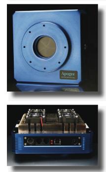
5 Camera views
6 CAMERA SUMMARY DESCRIPTION

7 CAMERA SPECS

8 CAMERA SPECS, cont.
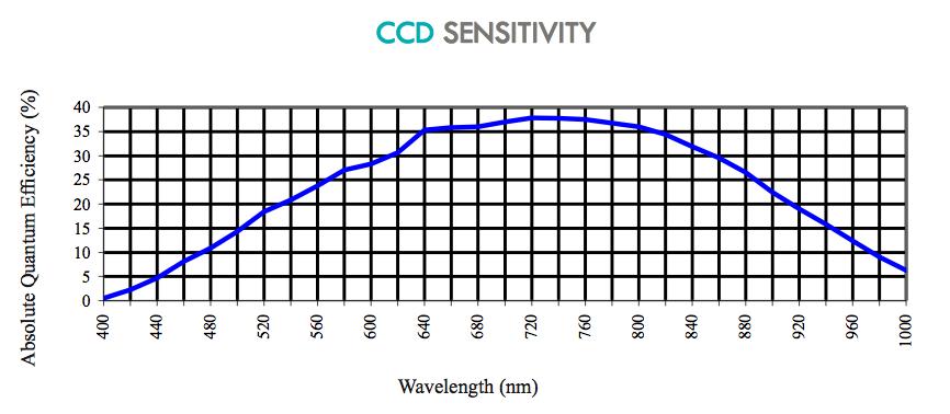
9 QUANTUM EFFICIENCY

10 Kirchhoff's Laws of Spectral Analysis continuum spectrum emission spectrum 1. An incandescent solid or high dense gas (such as a blackbody) produces a continuous spectrum. II. A hot low-density gas produces an emissionline spectrum. absorption spectrum III. A continuous spectrum source viewed through a cooler low-density gas produces an absorption-line spectrum.
11 DETECTION MODES Photon detectors: Produce a signal that depends on an individual photon change the quantum state of electrons in the detector, i.e. current/ voltage, chemical reactions or a pulse of free electrons (vacuum photomultipliers). Thermal detectors: Convert the energy of photons into heat. (IR, XR, Gamma)...bolometers.. Wave detectors: Measure interference. Radio and microwave.
12 EFFICIENCY Photography is highly inefficient. Quantum efficiency, QE = N det 100% indicates no photon lost. N in Photography has QE in the range 0.5-5% Solid state devices have QEs in the range 20-95%. Quantum yield is the # of detection events (i.e for CCD creation of a e-h pair) per incident photon. i.e. If a γ has energy less than 5 ev, the qy is 1 (recall 3.65 ev is the energy required to remove an electron in Si.

13 What are CCDs? From Steve Howell, Handbook of CCD Astronomy The rain collecting bucket array analogy: An array of buckets covering a surface collects water. After the rain, each bucket is transported to a belt where it is drained into a meter-bucket. The actual CCD starts with the photoelectric effect. Silicon can absorb photons of the right energy (band gap energy 1.14 ev. It can then absorb between 1.1 and 4 ev (11,000 to 3,000 Å).
14 CCD OPERATION Each pixel has a structure allowing applied voltages to be place in subpixel size electrodes: gates. The gate structures let the pixel collect freed electrons and hold them in a potential well until the end of the exposure. Typically there are three p/ pixel. The voltages are controlled by clock circuits with every third gate connected to the same clock. The gates are cycled to transfer the charges after exposure terminates and readout begins. The efficiency in the charge transferred is CTE.

15 CCD OPERATION Each pixel has a structure allowing applied voltages to be place in subpixel size electrodes: gates. The gate structures let the pixel collect freed electrons and hold them in a potential well until the end of the exposure. Typically there are three p/ pixel. The voltages are controlled by clock circuits with every third gate connected to the same clock. The gates are cycled to transfer the charges after exposure terminates and readout begins. The efficiency in the charge transferred is CTE.
16 CCD OPERATION II Each column in the array is connected in parallel. Once clock cycle moves each row up one column. The top one is is shifted off the array into the output shift register (horizontal shift register). Each pixel in the output register is measure as a voltage and converted into and output digital number. The sensed charge is amplified by an output amplifier. Their sensitivity is typically of 0.5 to 4 microv/e. The conversion of of the output voltage to a DN is counted as an Analog to Digital Unit (ADU). The amount of voltage needed to produce 1 ADU is the gain of the device. A typical CCD gain 10 e - /ADU (per 10 e - 1 ADU). The conversion is performed by and ADC. Notice that with size the time to complete the operation increases. There are many tricks.
17 CCD TYPES Surface channel vs buried channel In surface channel the transfer occurs on the surface between overlapping gates. transfer rates in video CCDs are MHz. Problems: traps due to impurities. (one way of eliminating this is through pre-flash or zero flat (raising the charge: the CCD needs to low level prior to exposure). Better solution is to use a buried channel architecture. Front-sided vs back sided illuminated CCDs Front sided: light illuminates the front; thickness is 300 microns. Susceptible to detection of cosmic rays.

18 FRONT SIDED ILLUMINATED PIXEL
19 Back sided illuminated Are thinned to >15 microns and illuminated from behind. No interference with the gates. Advantage is better QE, better response to shorter wavelengths photons (no need to go through the gates). Disadvantage shallower pixel wells. Interline and frame transfer Interline transfer CCDs have each column of pixels (active) paralleled by a shielded column of storage (inactive) pixels.

20 Interline and frame transfer

21 Antiblooming CCDs The full well capacity of a pixel is exceed and bleeding appears.
22 Other CCDs types Multipinned phase CCDs Typically for thermoelectrically cooled devices. It relies on the inversion of all the 3 clock voltages and doping of the 3 gates to lower the dark (thermal) current. Orthogonal transfer CCDs Pixels can be shifted horizontally as well as vertically. Lower QE. First used in image motion. Low light level They have an extended serial register, clocked at a higher voltage (40-60 V) allowing for a slight chance of avalanche multiplication of electrons, effectively increasing the gain. i.e. for 1% the gain=1.01 N where N i st he number of elements in the register. For a N= 500 the gain is 145.
23 More stuff Superconducting tunnel junctions UV and IR detection CMOS devices more commercial. Additional circuitry. QE low. CCD coatings Different coatings enhance sensitivity particularly in wavelengths were Si fails.
24 EXERCISES FOR LESSON I From Handbook of CCD Astronomy (page 34 2nd edition): Ex 2, Ex 3, Ex 5, Ex 6, Ex 21.
Charged-Coupled Devices
 Charged-Coupled Devices Charged-Coupled Devices Useful texts: Handbook of CCD Astronomy Steve Howell- Chapters 2, 3, 4.4 Measuring the Universe George Rieke - 3.1-3.3, 3.6 CCDs CCDs were invented in 1969
CCD Characteristics Lab
 CCD Characteristics Lab Observational Astronomy 6/6/07 1 Introduction In this laboratory exercise, you will be using the Hirsch Observatory s CCD camera, a Santa Barbara Instruments Group (SBIG) ST-8E.
Detectors for microscopy - CCDs, APDs and PMTs. Antonia Göhler. Nov 2014
 Detectors for microscopy - CCDs, APDs and PMTs Antonia Göhler Nov 2014 Detectors/Sensors in general are devices that detect events or changes in quantities (intensities) and provide a corresponding output,
Three Ways to Detect Light. We now establish terminology for photon detectors:
 Three Ways to Detect Light In photon detectors, the light interacts with the detector material to produce free charge carriers photon-by-photon. The resulting miniscule electrical currents are amplified
Properties of a Detector
 Properties of a Detector Quantum Efficiency fraction of photons detected wavelength and spatially dependent Dynamic Range difference between lowest and highest measurable flux Linearity detection rate
Introduction to CCD camera
 Observational Astronomy 2011/2012 Introduction to CCD camera Charge Coupled Device (CCD) photo sensor coupled to shift register Jörg R. Hörandel Radboud University Nijmegen http://particle.astro.ru.nl/goto.html?astropract1-1112
Optical/IR Observational Astronomy Detectors II. David Buckley, SAAO
 David Buckley, SAAO 1 The Next Revolution: Charge Couple Device Detectors (CCDs) 2 Optical/IR Observational Astronomy CCDs Integrated semi-conductor detector From photon detection (pair production) to
Two-phase full-frame CCD with double ITO gate structure for increased sensitivity
 Two-phase full-frame CCD with double ITO gate structure for increased sensitivity William Des Jardin, Steve Kosman, Neal Kurfiss, James Johnson, David Losee, Gloria Putnam *, Anthony Tanbakuchi (Eastman
Based on lectures by Bernhard Brandl
 Astronomische Waarneemtechnieken (Astronomical Observing Techniques) Based on lectures by Bernhard Brandl Lecture 10: Detectors 2 1. CCD Operation 2. CCD Data Reduction 3. CMOS devices 4. IR Arrays 5.
VII. IR Arrays & Readout VIII.CCDs & Readout. This lecture course follows the textbook Detection of
 Detection of Light VII. IR Arrays & Readout VIII.CCDs & Readout This lecture course follows the textbook Detection of Light 4-3-2016 by George Rieke, Detection Cambridge of Light Bernhard Brandl University
Three Ways to Detect Light. Following: Lord Rosse image of M33 vs. Hubble image demonstrate how critical detector technology is.
 Three Ways to Detect Light In photon detectors, the light interacts with the detector material to produce free charge carriers photon-by-photon. The resulting miniscule electrical currents are amplified
Introduction. Chapter 1
 1 Chapter 1 Introduction During the last decade, imaging with semiconductor devices has been continuously replacing conventional photography in many areas. Among all the image sensors, the charge-coupled-device
Charge-Coupled Device (CCD) Detectors pixel silicon chip electronics cryogenics
 Detectors pixel silicon chip electronics cryogenics") Charge-Coupled Device (CCD) Detectors As revolutionary in astronomy as the invention of the telescope and photography semiconductor detectors a collection of miniature photodiodes, each called a picture
Charge-Coupled Device (CCD) Detectors As revolutionary in astronomy as the invention of the telescope and photography semiconductor detectors a collection of miniature photodiodes, each called a picture
Charged Coupled Device (CCD) S.Vidhya
 S.Vidhya") Charged Coupled Device (CCD) S.Vidhya 02.04.2016 Sensor Physical phenomenon Sensor Measurement Output A sensor is a device that measures a physical quantity and converts it into a signal which can be read
Charged Coupled Device (CCD) S.Vidhya 02.04.2016 Sensor Physical phenomenon Sensor Measurement Output A sensor is a device that measures a physical quantity and converts it into a signal which can be read
An Introduction to CCDs. The basic principles of CCD Imaging is explained.
 An Introduction to CCDs. The basic principles of CCD Imaging is explained. Morning Brain Teaser What is a CCD? Charge Coupled Devices (CCDs), invented in the 1970s as memory devices. They improved the
CCD Analogy BUCKETS (PIXELS) HORIZONTAL CONVEYOR BELT (SERIAL REGISTER) VERTICAL CONVEYOR BELTS (CCD COLUMNS) RAIN (PHOTONS)
 HORIZONTAL CONVEYOR BELT (SERIAL REGISTER) VERTICAL CONVEYOR BELTS (CCD COLUMNS) RAIN (PHOTONS)") CCD Analogy RAIN (PHOTONS) VERTICAL CONVEYOR BELTS (CCD COLUMNS) BUCKETS (PIXELS) HORIZONTAL CONVEYOR BELT (SERIAL REGISTER) MEASURING CYLINDER (OUTPUT AMPLIFIER) Exposure finished, buckets now contain
CCD Analogy RAIN (PHOTONS) VERTICAL CONVEYOR BELTS (CCD COLUMNS) BUCKETS (PIXELS) HORIZONTAL CONVEYOR BELT (SERIAL REGISTER) MEASURING CYLINDER (OUTPUT AMPLIFIER) Exposure finished, buckets now contain
Photons and solid state detection
 Photons and solid state detection Photons represent discrete packets ( quanta ) of optical energy Energy is hc/! (h: Planck s constant, c: speed of light,! : wavelength) For solid state detection, photons
Fundamentals of CMOS Image Sensors
 CHAPTER 2 Fundamentals of CMOS Image Sensors Mixed-Signal IC Design for Image Sensor 2-1 Outline Photoelectric Effect Photodetectors CMOS Image Sensor(CIS) Array Architecture CIS Peripherals Design Considerations
Introduction. Cambridge University Press Handbook of CCD Astronomy: Second Edition Steve B. Howell Excerpt More information
 1 Introduction Silicon. This semiconductor material certainly has large implications on our life. Its uses are many, including silicon oil lubricants, implants to change our bodies outward appearance,
Lecture 29: Image Sensors. Computer Graphics and Imaging UC Berkeley CS184/284A
 Lecture 29: Image Sensors Computer Graphics and Imaging UC Berkeley Photon Capture The Photoelectric Effect Incident photons Ejected electrons Albert Einstein (wikipedia) Einstein s Nobel Prize in 1921
CHARGE-COUPLED DEVICE (CCD)
") CHARGE-COUPLED DEVICE (CCD) Definition A charge-coupled device (CCD) is an analog shift register, enabling analog signals, usually light, manipulation - for example, conversion into a digital value that
CHARGE-COUPLED DEVICE (CCD) Definition A charge-coupled device (CCD) is an analog shift register, enabling analog signals, usually light, manipulation - for example, conversion into a digital value that
The Charge-Coupled Device. Many overheads courtesy of Simon Tulloch
 The Charge-Coupled Device Astronomy 1263 Many overheads courtesy of Simon Tulloch smt@ing.iac.es Jan 24, 2013 What does a CCD Look Like? The fine surface electrode structure of a thick CCD is clearly visible
Ground-based optical auroral measurements
 Ground-based optical auroral measurements FYS 3610 Background Ground-based optical measurements provides a unique way to monitor spatial and temporal variation of auroral activity at high resolution up
Astronomy /6/15. In this Lecture: (Detector Technology) Nomenclature. Lecture 3: Introduction to CCD and CMOS Imaging Devices
 Nomenclature. Lecture 3: Introduction to CCD and CMOS Imaging Devices") Astronomy 3310 Lecture 3: Introduction to CCD and CMOS Imaging Devices Lecture 3 Astro 3310 1 In this Lecture: (Detector Technology) Introduc/on to Solid State Detectors CCD CMOS and IRFPA Basic CCD /
Astronomy 3310 Lecture 3: Introduction to CCD and CMOS Imaging Devices Lecture 3 Astro 3310 1 In this Lecture: (Detector Technology) Introduc/on to Solid State Detectors CCD CMOS and IRFPA Basic CCD /
IV DETECTORS. Daguerrotype of the Moon, John W. Draper. March 26, 1840 New York
 IV DETECTORS Lit.: C.R.Kitchin: Astrophysical Techniques, 2009 C.D.Mckay: CCD s in Astronomy, Ann.Rev. A.&A. 24, 1986 G.H.Rieke: Infrared Detector Arrays for Astronomy, Ann.Rev. A&A 45, 2007 up to 1837:
Page 1. Ground-based optical auroral measurements. Background. CCD All-sky Camera with filterwheel. Image intensifier
 Ground-based optical auroral measurements FYS 3610 Background Ground-based optical measurements provides a unique way to monitor spatial and temporal variation of auroral activity at high resolution up
Low Light Level CCD Performance and Issues
 Low Light Level CCD Performance and Issues Nagaraja Bezawada UK Astronomy Technology Centre 04 July 2007 Overview of the Talk Introduction to L3CCD (EM CCD) ULTRASPEC Performance and Issues New L3 CCD
An Introduction to Scientific Imaging C h a r g e - C o u p l e d D e v i c e s
 p a g e 2 S C I E N T I F I C I M A G I N G T E C H N O L O G I E S, I N C. Introduction to the CCD F u n d a m e n t a l s The CCD Imaging A r r a y An Introduction to Scientific Imaging C h a r g e -
How Does One Obtain Spectral/Imaging Information! "
 How Does One Obtain Spectral/Imaging Information! How do we measure the position, energy, and arrival time of! an X-ray photon?! " What we observe depends on the instruments that one observes with!" In
Basic CCD imaging CCD/CMOS Cameras
 Pedro Ré (2018) http:/re.apaaweb.com Basic CCD imaging CCD/CMOS Cameras There are basically five different kinds of digital cameras: 1. Dedicated, Cooled Astronomical CCD Cameras (CCD) 2. Digital SLR Cameras
Gamma Spectrometer Initial Project Proposal
 Gamma Spectrometer Initial Project Proposal Group 9 Aman Kataria Johnny Klarenbeek Dean Sullivan David Valentine Introduction There are currently two main types of gamma radiation detectors used for gamma
INTRODUCTION TO CCD IMAGING
 ASTR 1030 Astronomy Lab 85 Intro to CCD Imaging INTRODUCTION TO CCD IMAGING SYNOPSIS: In this lab we will learn about some of the advantages of CCD cameras for use in astronomy and how to process an image.
STA1600LN x Element Image Area CCD Image Sensor
 ST600LN 10560 x 10560 Element Image Area CCD Image Sensor FEATURES 10560 x 10560 Photosite Full Frame CCD Array 9 m x 9 m Pixel 95.04mm x 95.04mm Image Area 100% Fill Factor Readout Noise 2e- at 50kHz
Minimizes reflection losses from UV-IR; Optional AR coatings & wedge windows are available.
 Now Powered by LightField PyLoN:2K 2048 x 512 The PyLoN :2K is a controllerless, cryogenically-cooled CCD camera designed for quantitative scientific spectroscopy applications demanding the highest possible
Lecture 18: Photodetectors
 Lecture 18: Photodetectors Contents 1 Introduction 1 2 Photodetector principle 2 3 Photoconductor 4 4 Photodiodes 6 4.1 Heterojunction photodiode.................... 8 4.2 Metal-semiconductor photodiode................
Digital Imaging Rochester Institute of Technology
 Digital Imaging 1999 Rochester Institute of Technology So Far... camera AgX film processing image AgX photographic film captures image formed by the optical elements (lens). Unfortunately, the processing
Astro-photography. Daguerreotype: on a copper plate
 AST 1022L Astro-photography 1840-1980s: Photographic plates were astronomers' main imaging tool At right: first ever picture of the full moon, by John William Draper (1840) Daguerreotype: exposure using
Light gathering Power: Magnification with eyepiece:
 Telescopes Light gathering Power: The amount of light that can be gathered by a telescope in a given amount of time: t 1 /t 2 = (D 2 /D 1 ) 2 The larger the diameter the smaller the amount of time. If
TDI Imaging: An Efficient AOI and AXI Tool
 TDI Imaging: An Efficient AOI and AXI Tool Yakov Bulayev Hamamatsu Corporation Bridgewater, New Jersey Abstract As a result of heightened requirements for quality, integrity and reliability of electronic
Charge Coupled Devices. C. A. Griffith, Class Notes, PTYS 521, 2016 Not for distribution.
 Charge Coupled Devices C. A. Griffith, Class Notes, PTYS 521, 2016 Not for distribution. 1 1. Introduction While telescopes are able to gather more light from a distance source than does the naked eye,
Where detectors are used in science & technology
 Lecture 9 Outline Role of detectors Photomultiplier tubes (photoemission) Modulation transfer function Photoconductive detector physics Detector architecture Where detectors are used in science & technology
Detailed Characterisation of a New Large Area CCD Manufactured on High Resistivity Silicon
 Detailed Characterisation of a New Large Area CCD Manufactured on High Resistivity Silicon Mark S. Robbins *, Pritesh Mistry, Paul R. Jorden e2v technologies Ltd, 106 Waterhouse Lane, Chelmsford, Essex
EE 392B: Course Introduction
 EE 392B Course Introduction About EE392B Goals Topics Schedule Prerequisites Course Overview Digital Imaging System Image Sensor Architectures Nonidealities and Performance Measures Color Imaging Recent
Overview. Charge-coupled Devices. MOS capacitor. Charge-coupled devices. Charge-coupled devices:
 Overview Charge-coupled Devices Charge-coupled devices: MOS capacitors Charge transfer Architectures Color Limitations 1 2 Charge-coupled devices MOS capacitor The most popular image recording technology
Last class. This class. CCDs Fancy CCDs. Camera specs scmos
 CCDs and scmos Last class CCDs Fancy CCDs This class Camera specs scmos Fancy CCD cameras: -Back thinned -> higher QE -Unexposed chip -> frame transfer -Electron multiplying -> higher SNR -Fancy ADC ->
IT FR R TDI CCD Image Sensor
 4k x 4k CCD sensor 4150 User manual v1.0 dtd. August 31, 2015 IT FR 08192 00 R TDI CCD Image Sensor Description: With the IT FR 08192 00 R sensor ANDANTA GmbH builds on and expands its line of proprietary
Welcome to: LMBR Imaging Workshop. Imaging Fundamentals Mike Meade, Photometrics
 Welcome to: LMBR Imaging Workshop Imaging Fundamentals Mike Meade, Photometrics Introduction CCD Fundamentals Typical Cooled CCD Camera Configuration Shutter Optic Sealed Window DC Voltage Serial Clock
A Summary of Charge-Coupled Devices for Astronomy
 PUBLICATIONS OF THE ASTRONOMICAL SOCIETY OF THE PACIFIC, 127:1097 1104, 2015 November 2015. The Astronomical Society of the Pacific. All rights reserved. Printed in U.S.A. A Summary of Charge-Coupled Devices
Part I. CCD Image Sensors
 Part I CCD Image Sensors 2 Overview of CCD CCD is the abbreviation for charge-coupled device. CCD image sensors are silicon-based integrated circuits (ICs), consisting of a dense matrix of photodiodes
3/5/17. Detector Basics. Quantum Efficiency (QE) and Spectral Response. Quantum Efficiency (QE) and Spectral Response
 and Spectral Response. Quantum Efficiency (QE) and Spectral Response") 3/5/17 Detector Basics The purpose of any detector is to record the light collected by the telescope. All detectors transform the incident radiation into a some other form to create a permanent record,
3/5/17 Detector Basics The purpose of any detector is to record the light collected by the telescope. All detectors transform the incident radiation into a some other form to create a permanent record,
STA3600A 2064 x 2064 Element Image Area CCD Image Sensor
 ST600A 2064 x 2064 Element Image Area CCD Image Sensor FEATURES 2064 x 2064 CCD Image Array 15 m x 15 m Pixel 30.96 mm x 30.96 mm Image Area Near 100% Fill Factor Readout Noise Less Than 3 Electrons at
the need for an intensifier
 * The LLLCCD : Low Light Imaging without the need for an intensifier Paul Jerram, Peter Pool, Ray Bell, David Burt, Steve Bowring, Simon Spencer, Mike Hazelwood, Ian Moody, Neil Catlett, Philip Heyes Marconi
In the name of God, the most merciful Electromagnetic Radiation Measurement
 In the name of God, the most merciful Electromagnetic Radiation Measurement In these slides, many figures have been taken from the Internet during my search in Google. Due to the lack of space and diversity
Characterisation of a CMOS Charge Transfer Device for TDI Imaging
 Preprint typeset in JINST style - HYPER VERSION Characterisation of a CMOS Charge Transfer Device for TDI Imaging J. Rushton a, A. Holland a, K. Stefanov a and F. Mayer b a Centre for Electronic Imaging,
Digital camera. Sensor. Memory card. Circuit board
 Digital camera Circuit board Memory card Sensor Detector element (pixel). Typical size: 2-5 m square Typical number: 5-20M Pixel = Photogate Photon + Thin film electrode (semi-transparent) Depletion volume
a simple optical imager
 Imagers and Imaging a simple optical imager Here s one on our 61-Inch Telescope Here s one on our 61-Inch Telescope filter wheel in here dewar preamplifier However, to get a large field we cannot afford
CCD1600A Full Frame CCD Image Sensor x Element Image Area
 - 1 - General Description CCD1600A Full Frame CCD Image Sensor 10560 x 10560 Element Image Area General Description The CCD1600 is a 10560 x 10560 image element solid state Charge Coupled Device (CCD)
Cameras CS / ECE 181B
 Cameras CS / ECE 181B Image Formation Geometry of image formation (Camera models and calibration) Where? Radiometry of image formation How bright? What color? Examples of cameras What is a Camera? A camera
Submillimeter (continued)
") Submillimeter (continued) Dual Polarization, Sideband Separating Receiver Dual Mixer Unit The 12-m Receiver Here is where the receiver lives, at the telescope focus Receiver Performance T N (noise temperature)
Submillimeter (continued) Dual Polarization, Sideband Separating Receiver Dual Mixer Unit The 12-m Receiver Here is where the receiver lives, at the telescope focus Receiver Performance T N (noise temperature)
ABSTRACT. Supported by U.S. DoE grant No. DE-FG02-96ER54375
 ABSTRACT A CCD imaging system is currently being developed for T e (,t) and bolometric measurements on the Pegasus Toroidal Experiment. Soft X-rays (E
Image sensor combining the best of different worlds
 Image sensors and vision systems Image sensor combining the best of different worlds First multispectral time-delay-and-integration (TDI) image sensor based on CCD-in-CMOS technology. Introduction Jonathan
Components of Optical Instruments
 Components of Optical Instruments General Design of Optical Instruments Sources of Radiation Wavelength Selectors (Filters, Monochromators, Interferometers) Sample Containers Radiation Transducers (Detectors)
PRELIMINARY. CCD 3041 Back-Illuminated 2K x 2K Full Frame CCD Image Sensor FEATURES
 CCD 3041 Back-Illuminated 2K x 2K Full Frame CCD Image Sensor FEATURES 2048 x 2048 Full Frame CCD 15 µm x 15 µm Pixel 30.72 mm x 30.72 mm Image Area 100% Fill Factor Back Illuminated Multi-Pinned Phase
Ultra-high resolution 14,400 pixel trilinear color image sensor
 Ultra-high resolution 14,400 pixel trilinear color image sensor Thomas Carducci, Antonio Ciccarelli, Brent Kecskemety Microelectronics Technology Division Eastman Kodak Company, Rochester, New York 14650-2008
Simulation of High Resistivity (CMOS) Pixels
 Pixels") Simulation of High Resistivity (CMOS) Pixels Stefan Lauxtermann, Kadri Vural Sensor Creations Inc. AIDA-2020 CMOS Simulation Workshop May 13 th 2016 OUTLINE 1. Definition of High Resistivity Pixel Also
Simulation of High Resistivity (CMOS) Pixels Stefan Lauxtermann, Kadri Vural Sensor Creations Inc. AIDA-2020 CMOS Simulation Workshop May 13 th 2016 OUTLINE 1. Definition of High Resistivity Pixel Also
Image acquisition. In both cases, the digital sensing element is one of the following: Line array Area array. Single sensor
 Image acquisition Digital images are acquired by direct digital acquisition (digital still/video cameras), or scanning material acquired as analog signals (slides, photographs, etc.). In both cases, the
Receiver Performance and Comparison of Incoherent (bolometer) and Coherent (receiver) detection
 and Coherent (receiver) detection") At ev gap /h the photons have sufficient energy to break the Cooper pairs and the SIS performance degrades. Receiver Performance and Comparison of Incoherent (bolometer) and Coherent (receiver) detection
At ev gap /h the photons have sufficient energy to break the Cooper pairs and the SIS performance degrades. Receiver Performance and Comparison of Incoherent (bolometer) and Coherent (receiver) detection
Lecture 8 Optical Sensing. ECE 5900/6900 Fundamentals of Sensor Design
 ECE 5900/6900: Fundamentals of Sensor Design Lecture 8 Optical Sensing 1 Optical Sensing Q: What are we measuring? A: Electromagnetic radiation labeled as Ultraviolet (UV), visible, or near,mid-, far-infrared
Week 9: Chap.13 Other Semiconductor Material
 Week 9: Chap.13 Other Semiconductor Material Exam Other Semiconductors and Geometries -- Why --- CZT properties -- Silicon Structures --- CCD s Gamma ray Backgrounds The MIT Semiconductor Subway (of links
Detection Beyond 100µm Photon detectors no longer work ("shallow", i.e. low excitation energy, impurities only go out to equivalent of
 Detection Beyond 100µm Photon detectors no longer work ("shallow", i.e. low excitation energy, impurities only go out to equivalent of 100µm) A few tricks let them stretch a little further (like stressing)
Spectroscopy in the UV and Visible: Instrumentation. Spectroscopy in the UV and Visible: Instrumentation
 Spectroscopy in the UV and Visible: Instrumentation Typical UV-VIS instrument 1 Source - Disperser Sample (Blank) Detector Readout Monitor the relative response of the sample signal to the blank Transmittance
ACTIVE PIXEL SENSORS VS. CHARGE-COUPLED DEVICES
 ACTIVE PIXEL SENSORS VS. CHARGE-COUPLED DEVICES Dr. Eric R. Fossum Imaging Systems Section Jet Propulsion Laboratory, California Institute of Technology (818) 354-3128 1993 IEEE Workshop on CCDs and Advanced
3/27/17. Detector Basics. Quantum Efficiency (QE) and Spectral Response. Quantum Efficiency (QE) and Spectral Response
 and Spectral Response. Quantum Efficiency (QE) and Spectral Response") 3/27/17 Detector Basics The purpose of any detector is to record the light collected by the telescope. All detectors transform the incident radiation into a some other form to create a permanent record,
3/27/17 Detector Basics The purpose of any detector is to record the light collected by the telescope. All detectors transform the incident radiation into a some other form to create a permanent record,
FUTURE PROSPECTS FOR CMOS ACTIVE PIXEL SENSORS
 FUTURE PROSPECTS FOR CMOS ACTIVE PIXEL SENSORS Dr. Eric R. Fossum Jet Propulsion Laboratory Dr. Philip H-S. Wong IBM Research 1995 IEEE Workshop on CCDs and Advanced Image Sensors April 21, 1995 CMOS APS
CCD47-10 NIMO Back Illuminated Compact Pack High Performance CCD Sensor
 CCD47-10 NIMO Back Illuminated Compact Pack High Performance CCD Sensor FEATURES 1024 by 1024 Nominal (1056 by 1027 Usable Pixels) Image area 13.3 x 13.3mm Back Illuminated format for high quantum efficiency
J. Janesick, S.A. Collins, and E.R. Fossum Imaging Systems Section Jet Propulsion Laboratory Pasadena, CA 91109
 Scientific CCD Technology at JPL J. Janesick, S.A. Collins, and E.R. Fossum maging Systems Section Jet Propulsion Laboratory Pasadena, CA 91109 ntroduction Charge-coupled devices (CCOs) were recognized
CCD reductions techniques
 CCD reductions techniques Origin of noise Noise: whatever phenomena that increase the uncertainty or error of a signal Origin of noises: 1. Poisson fluctuation in counting photons (shot noise) 2. Pixel-pixel
Marconi Applied Technologies CCD39-01 Back Illuminated High Performance CCD Sensor
 Marconi Applied Technologies CCD39-01 Back Illuminated High Performance CCD Sensor FEATURES * 80 by 80 1:1 Image Format * Image Area 1.92 x 1.92 mm * Split-frame Transfer Operation * 24 mm Square Pixels
Cooled cameras for scientific applications and astronomy. Ian Alderton Alrad Imaging division of Alrad Instruments Ltd
 Cooled cameras for scientific applications and astronomy Ian Alderton Alrad Imaging division of Alrad Instruments Ltd www.alrad.co.uk History 1970 - started as Wenzel Elektronic UK in NIM modules and radiation
Fully depleted, thick, monolithic CMOS pixels with high quantum efficiency
 Fully depleted, thick, monolithic CMOS pixels with high quantum efficiency Andrew Clarke a*, Konstantin Stefanov a, Nicholas Johnston a and Andrew Holland a a Centre for Electronic Imaging, The Open University,
X-ray Detectors: What are the Needs?
 X-ray Detectors: What are the Needs? Sol M. Gruner Physics Dept. & Cornell High Energy Synchrotron Source (CHESS) Ithaca, NY 14853 smg26@cornell.edu 1 simplified view of the Evolution of Imaging Synchrotron
THE CCD RIDDLE REVISTED: SIGNAL VERSUS TIME LINEAR SIGNAL VERSUS VARIANCE NON-LINEAR
 THE CCD RIDDLE REVISTED: SIGNAL VERSUS TIME LINEAR SIGNAL VERSUS VARIANCE NON-LINEAR Mark Downing 1, Peter Sinclaire 1. 1 ESO, Karl Schwartzschild Strasse-2, 85748 Munich, Germany. ABSTRACT The photon
Pocket Pumped Image Analysis Ivan Kotov Brookhaven National Laboratory
 Pocket Pumped Image Analysis Ivan Kotov Brookhaven National Laboratory Instrumentation Division Seminar November 13, 2013 1 CCD Readout Architecture Terms Charge motion Image area (exposed to light) Parallel
CCD30 11 Back Illuminated High Performance CCD Sensor
 CCD30 11 Back Illuminated High Performance CCD Sensor FEATURES * 1024 by 256 Pixel Format * 26 mm Square Pixels * Image Area 26.6 x 6.7 mm * Wide Dynamic Range * Symmetrical Anti-static Gate Protection
Engineering Medical Optics BME136/251 Winter 2018
 Engineering Medical Optics BME136/251 Winter 2018 Monday/Wednesday 2:00-3:20 p.m. Beckman Laser Institute Library, MSTB 214 (lab) *1/17 UPDATE Wednesday, 1/17 Optics and Photonic Devices III: homework
Active Pixel Sensors Fabricated in a Standard 0.18 um CMOS Technology
 Active Pixel Sensors Fabricated in a Standard.18 um CMOS Technology Hui Tian, Xinqiao Liu, SukHwan Lim, Stuart Kleinfelder, and Abbas El Gamal Information Systems Laboratory, Stanford University Stanford,
Detectors that cover a dynamic range of more than 1 million in several dimensions
 Detectors that cover a dynamic range of more than 1 million in several dimensions Detectors for Astronomy Workshop Garching, Germany 10 October 2009 James W. Beletic Teledyne Providing the best images
Abstract. Preface. Acknowledgments
 Contents Abstract Preface Acknowledgments iv v vii 1 Introduction 1 1.1 A Very Brief History of Visible Detectors in Astronomy................ 1 1.2 The CCD: Astronomy s Champion Workhorse......................
CMOS Today & Tomorrow
 CMOS Today & Tomorrow Uwe Pulsfort TDALSA Product & Application Support Overview Image Sensor Technology Today Typical Architectures Pixel, ADCs & Data Path Image Quality Image Sensor Technology Tomorrow
Silicon sensors for radiant signals. D.Sc. Mikko A. Juntunen
 Silicon sensors for radiant signals D.Sc. Mikko A. Juntunen 2017 01 16 Today s outline Introduction Basic physical principles PN junction revisited Applications Light Ionizing radiation X-Ray sensors in
Micro-sensors - what happens when you make "classical" devices "small": MEMS devices and integrated bolometric IR detectors
 Micro-sensors - what happens when you make "classical" devices "small": MEMS devices and integrated bolometric IR detectors Dean P. Neikirk 1 MURI bio-ir sensors kick-off 6/16/98 Where are the targets
What an Observational Astronomer needs to know!
 What an Observational Astronomer needs to know! IRAF:Photometry D. Hatzidimitriou Masters course on Methods of Observations and Analysis in Astronomy Basic concepts Counts how are they related to the actual
High Resolution 640 x um Pitch InSb Detector
 High Resolution 640 x 512 15um Pitch InSb Detector Chen-Sheng Huang, Bei-Rong Chang, Chien-Te Ku, Yau-Tang Gau, Ping-Kuo Weng* Materials & Electro-Optics Division National Chung Shang Institute of Science
DV420 SPECTROSCOPY. issue 2 rev 1 page 1 of 5m. associated with LN2
 SPECTROSCOPY Andor s DV420 CCD cameras offer the best price/performance for a wide range of spectroscopy applications. The 1024 x 256 array with 26µm 2 pixels offers the best dynamic range versus resolution.
Image Formation and Camera Design
 Image Formation and Camera Design Spring 2003 CMSC 426 Jan Neumann 2/20/03 Light is all around us! From London & Upton, Photography Conventional camera design... Ken Kay, 1969 in Light & Film, TimeLife
Detectors for AXIS. Eric D. Miller Catherine Grant (MIT)
") Detectors for AXIS Eric D. Miller Catherine Grant (MIT) Outline detector technology and capabilities CCD (charge coupled device) APS (active pixel sensor) notional AXIS detector background particle environment
Detectors for AXIS Eric D. Miller Catherine Grant (MIT) Outline detector technology and capabilities CCD (charge coupled device) APS (active pixel sensor) notional AXIS detector background particle environment
Digital Photographs, Image Sensors and Matrices
 Digital Photographs, Image Sensors and Matrices Digital Camera Image Sensors Electron Counts Checkerboard Analogy Bryce Bayer s Color Filter Array Mosaic. Image Sensor Data to Matrix Data Visualization
Tunable wideband infrared detector array for global space awareness
 Tunable wideband infrared detector array for global space awareness Jonathan R. Andrews 1, Sergio R. Restaino 1, Scott W. Teare 2, Sanjay Krishna 3, Mike Lenz 3, J.S. Brown 3, S.J. Lee 3, Christopher C.
E2V Technologies CCD42-80 Back Illuminated High Performance CCD Sensor
 E2V Technologies CCD42-80 Back Illuminated High Performance CCD Sensor FEATURES * 2048 by 4096 Pixel Format * 1.5 mm Square Pixels * Image Area 27.6 x 55. mm * Wide Dynamic Range * Symmetrical Anti-static
DETECTORS Important characteristics: 1) Wavelength response 2) Quantum response how light is detected 3) Sensitivity 4) Frequency of response
 Wavelength response 2) Quantum response how light is detected 3) Sensitivity 4) Frequency of response") DETECTORS Important characteristics: 1) Wavelength response 2) Quantum response how light is detected 3) Sensitivity 4) Frequency of response (response time) 5) Stability 6) Cost 7) convenience Photoelectric
DETECTORS Important characteristics: 1) Wavelength response 2) Quantum response how light is detected 3) Sensitivity 4) Frequency of response (response time) 5) Stability 6) Cost 7) convenience Photoelectric