Silicon sensors for radiant signals. D.Sc. Mikko A. Juntunen
|
|
|
- Gordon McLaughlin
- 5 years ago
- Views:
Transcription
1 Silicon sensors for radiant signals D.Sc. Mikko A. Juntunen
2 Today s outline Introduction Basic physical principles PN junction revisited Applications Light Ionizing radiation X-Ray sensors in medical applications Group discussion about sensitivity of radiant sensors
3 Introduction to radiation sensors The very first sensors were radiant sensors well known technology Radiant signals can be divided into two groups Electromagnetic radiation (photodetectors, X-ray detectors) Nuclear-particle radiation (particle detectors) (Is there really a difference? Wave-particle duality ) Application areas range from automotive twilight detectors through optical communications, bioluminescence and radiation dosimetry to medical imaging and particle physics. These were just examples, but all require a detector to convert radiation into an electrical signal. Selection criteria: wavelength and intensity of light
4 Electromagnetic Radiation E = hn = hc p / l Intensity, Phase
5 Electromagnetic radiation
6 Similar to solar cells photodetectors benefit from AR coatings The graph below shows the reflectivity of a special image sensor (CCD). The sensor was designed for a maximum blue response and it has an anti-reflective coating optimised to work at 400nm. At this wavelength the reflectivity falls to approximately 1%.

7 Photoelectric effect Incoming photon creates an electron-hole pair photoconductivity In the absence of an external electric field the hole and electron will quickly recombine and be lost. An electric field is introduced to sweep these charge carriers apart and prevent recombination light generates open circuit voltage Back surface Conductance band Band gap 1,12 ev Valence band P-type Depletion region Hole Released electron N-type Front surface V oc ~0,6 V Photon Thermally generated electrons are indistinguishable from photo-generated electrons. They constitute a noise source known as Dark Current. Lowering the operation temperature Dark Current can be minimised.
8 Quantum efficiency (QE) QE is the amount charge carrier collected compared to the amount of photons entering the detector surface If each photon generates a charge, and each charge is collected, QE = 1 = 100% External losses (EQE) Reflectance from the surface Absorption in the material above the depletion region (AR coating, metal contacts ) Internal losses (IQE) Absorption coefficient of the material (band gap) Recombination (defects) For better QE Maximize the depletiond region width Minimize the dead layer width above Maximize collection efficiency within device

9 Factors affecting quantum efficiency: Loss of photons into entry window, typically nitride and oxide => make it thin, optically optimized Loss of photons before entering depletion region => make implatation thin to extend depletion close to surface Almost one electron released per photon nm With photon energy > 1,12 ev, extra energy is lost in electron kinetic energy => warming up the diode For energies less than 1,12 ev, silicon is transparent Loss of photons through depletion region => make depletion deep enough => use high purity low resistivity substrate materials
10 Basic readout schemes (1/2) Light current/charge integrator Output voltage ~ accumulated charge Volatage recorded periodically, and resetting to start new collection cycle Current to voltage follower: Output voltage ~ input current = light intensity
11 Basic readout schemes (2/2) Basic circuit for pulse counting: short fast pulse charges the capacitor resistor will reset it automatically Output voltage peaks shortly peak hight ~ incoming pulse energy typically followed by a shaping amplifier + MCA, or a counter
12 Applications
13 Photoconductor The most simple photodetector Based on photoconductivity Operation principle: Incoming light changes the resistivity, which can be measured Used to measure light intensity in simple applications Optimization The detector thickness d must be much greater than the inverse of the absorption coefficient (for total absorption) A compromise between the amplification and the response time of the photoconductor The photoionization cross-section must be as large as possible


14 Photodiodes Light creates e-h pairs Revese biased diode Benefits of PIN vs. PN Sensitivity (larger photosensitive volume) Higher lifetime and mobility High breakdown voltage, high reverse bias allowed Speed (smaller capacitance)
15 Other types of photosensors

16 Impact ionisation (avalanche multiplication) Highly energetic carrier donates its excess energy for another carrier creating a new electronhole pair Due to the high electric field the new e-h pair can generate further new e-h pairs

17 Avalanche photodiodes Operation principle Large reverse bias voltage accelerates the minority carriers multiple electron-hole pairs created Properties The quantum efficiency is higher than in normal photodiodes The response speed is shorter Uniform gain Excellent short wavelength sensitivity detection of low-level light at high speed - noise?
18 Quadrant photodiodes Four photodetectors positioned in the quadrant geometry Applications in laser alignment and light/satellite positioning Light-impenetrable window over the device -> light does not illuminate equally the detectors
19 Position-sensitive detectors Sun position photodetectors Based on quadrant photodiodes a min = arctan(2 h/ W) a min < arctan(2 h/ 3 W)


20 CCD (charge coupled device) image sensor CCDs work by converting light into a pattern of electronic charge in a silicon chip. This pattern of charge is converted into a video waveform, digitised and stored as an image file on a computer.

21 Charge-coupled devices Consist of an array of MOS-capacitors An image builds up that consists of a pattern of electric charge. Charge acts as a signal. At the end of the exposure this pattern is then transferred, pixel at a time, by way of the serial register to the onchip amplifier Charge is transferred by applying gate voltages Applications of 21silicon sensors for
22 Charge collection incoming photons pixel boundary pixel boundary Charge packet n-type silicon p-type silicon Electrode Structure SiO2 Insulating layer
23 Charge Transfer in a CCD V 0V -5V +5V 0V -5V +5V 0V -5V Time-slice shown in diagram
24 Charge Transfer in a CCD V 0V -5V +5V 0V -5V +5V 0V -5V
25 Charge Transfer in a CCD V 0V -5V +5V 0V -5V +5V 0V -5V
26 Charge Transfer in a CCD V 0V -5V +5V 0V -5V +5V 0V -5V
27 Charge Transfer in a CCD V 0V -5V +5V 0V -5V +5V 0V -5V
28 Charge Transfer in a CCD 7. Charge packet from subsequent pixel enters from left as first pixel exits to the right V 0V -5V +5V 0V -5V +5V 0V -5V
29 Charge Transfer in a CCD V 0V -5V +5V 0V -5V +5V 0V -5V

30 Fabrication of CCD CCDs are are manufactured on silicon wafers using the same photo-lithographic techniques used to manufacture computer chips. Scientific CCDs are very big,only a few can be fitted onto a wafer. This is one reason that they are so costly. Don Groom LBNL
31 Thick Front-side Illuminated CCD Incoming photons p-type silicon 625mm n-type silicon Silicon dioxide insulating layer Polysilicon electrodes These are cheap to produce using conventional wafer fabrication techniques. They are used in consumer imaging applications. Even though not all the photons are detected, these devices are still more sensitive than photographic film. They have a low Quantum Efficiency due to the reflection and absorption of light in the surface electrodes. Very poor blue response. The electrode structure prevents the use of an Anti-reflective coating that would otherwise boost performance.
32 Thinned back-side illuminated CCD 15mm Incoming photons Anti-reflective (AR) coating p-type silicon n-type silicon Silicon dioxide insulating layer Polysilicon electrodes The silicon is chemically etched and polished down to a thickness of about 15microns. Light enters from the rear and so the electrodes do not obstruct the photons. The QE can approach 100%. These are very expensive to produce since the thinning is a non-standard process that reduces the chip yield. These thinned CCDs become transparent to near infra-red light and the red response is poor. Response can be boosted by the application of an anti-reflective coating on the thinned rear-side. These coatings do not work so well for thick CCDs due to the surface bumps created by the surface electrodes.
33 Comparision of quantum efficiency

34 CMOS vs. CCD
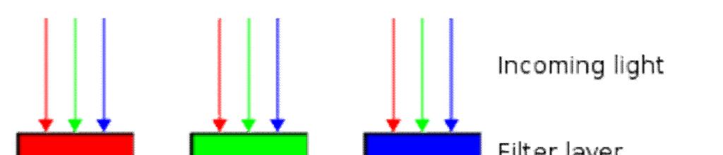
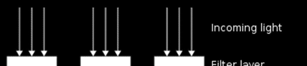
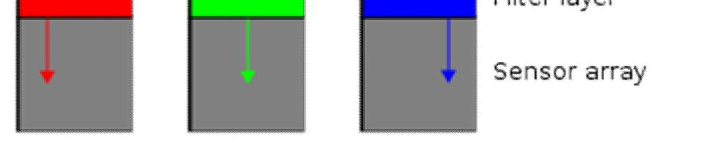

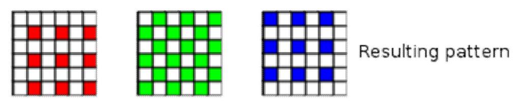
35 Color separation
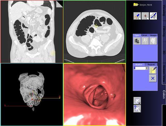
36 Nuclear particle radiation detectors Nuclear particles create electronhole pairs within the detector Electric field separates the electrons and holes and they are collected from their respective contacts High energy particles may create 85 electron-hole pairs per micron when penetrating inside the silicon wafer In order to achieve a good signal to noise level a sensitive volume of a few hundred cubic microns is therefore required


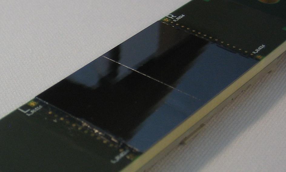
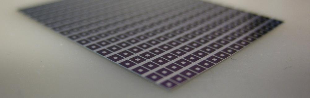
37 Development of tileable silicon photodiodes for X-ray imaging

38 CT = Computed Tomography

39 I( x) = I exp( -a x) os N j wij mi = -ln i= 1 I 0 I

40 CT in diagnostics 1/4 Sharpness
41 CT in diangostics 2/4

42 CT in diagnostics 3/4 Dynamic range?

43 CT in diagnostics 4/4 54-year-old female No obesity Atypical chest pain Hypercholesterolemia Family history of coronary artery disease Cardiac CT demonstrate healthy heart Resolution?


44 Detectors the eyes of the machine multi slice imaging Photodiode matrix covered with scintillator to convert X-rays to visible light Wiring from the edges


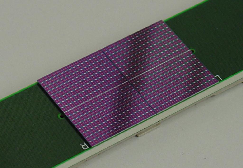
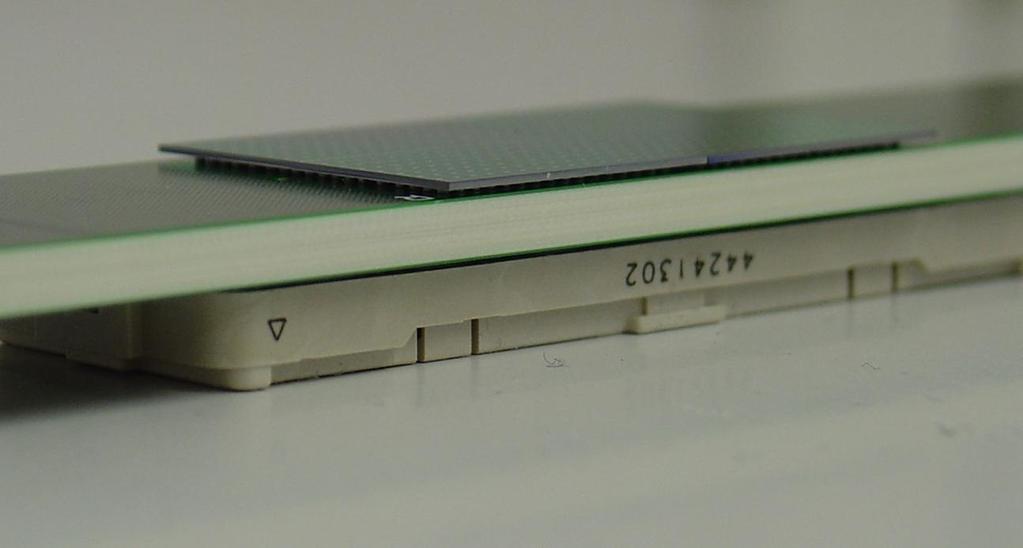
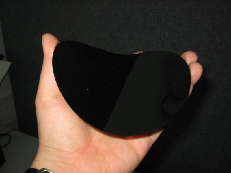
45 Why tileable detectors Larger detectors needed Desire to image the whole organ in one rotation Need to connect from edges prevent expansion Thickness about 25 µm, half of human hair How to make detectors that can be tiled next to each other to form arbitrarily large detecting surface


46 Tileable technologies developed 1/3 Cathode Readout Cross talk? UK patent GB B, US Patent 7,375,340 B2, etc.
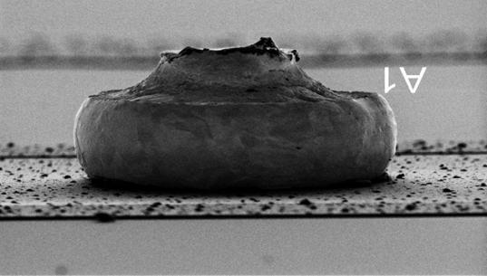
47 Tileable technologies developed 2/3 Through Silicon Vias 50 µm Al SiO SiO 2 2 0,002 mm 2 p anode area Poly Si conductor n type Sin type Si substrate substrate p anode area n type Si substrate Al anode contact Al cathode contact UK patent GB B


48 Method Etching the T Etching through PolySi fill Grind and polish Poly Si Scale: hair 2 µm SiO 2 Si Si Scale: red blood cells UK Patent GB B
49 Demonstration module with TSV s
50 Tileable technologies developed 3/3 Back Side Illuminated Diodes Light Signal (charge) is generated within first few 1 µm of the diode back side. N+ - implantation N+ - implntation Diffusion Cross talk? Diode implantation Al SiO 2 A

51 Long Distance Diffusion Several ms charge carrier lifetime Several mm diffusion distance Treatment of back surface to reflect holes Collecting diode on front surface => virtually all signaali gets collected Still, thinning to ~100 µm improves the outcome
52
53
54
The Charge-Coupled Device. Many overheads courtesy of Simon Tulloch
 The Charge-Coupled Device Astronomy 1263 Many overheads courtesy of Simon Tulloch smt@ing.iac.es Jan 24, 2013 What does a CCD Look Like? The fine surface electrode structure of a thick CCD is clearly visible
CCD Analogy BUCKETS (PIXELS) HORIZONTAL CONVEYOR BELT (SERIAL REGISTER) VERTICAL CONVEYOR BELTS (CCD COLUMNS) RAIN (PHOTONS)
 HORIZONTAL CONVEYOR BELT (SERIAL REGISTER) VERTICAL CONVEYOR BELTS (CCD COLUMNS) RAIN (PHOTONS)") CCD Analogy RAIN (PHOTONS) VERTICAL CONVEYOR BELTS (CCD COLUMNS) BUCKETS (PIXELS) HORIZONTAL CONVEYOR BELT (SERIAL REGISTER) MEASURING CYLINDER (OUTPUT AMPLIFIER) Exposure finished, buckets now contain
CCD Analogy RAIN (PHOTONS) VERTICAL CONVEYOR BELTS (CCD COLUMNS) BUCKETS (PIXELS) HORIZONTAL CONVEYOR BELT (SERIAL REGISTER) MEASURING CYLINDER (OUTPUT AMPLIFIER) Exposure finished, buckets now contain
An Introduction to CCDs. The basic principles of CCD Imaging is explained.
 An Introduction to CCDs. The basic principles of CCD Imaging is explained. Morning Brain Teaser What is a CCD? Charge Coupled Devices (CCDs), invented in the 1970s as memory devices. They improved the
Fundamentals of CMOS Image Sensors
 CHAPTER 2 Fundamentals of CMOS Image Sensors Mixed-Signal IC Design for Image Sensor 2-1 Outline Photoelectric Effect Photodetectors CMOS Image Sensor(CIS) Array Architecture CIS Peripherals Design Considerations
Lecture 18: Photodetectors
 Lecture 18: Photodetectors Contents 1 Introduction 1 2 Photodetector principle 2 3 Photoconductor 4 4 Photodiodes 6 4.1 Heterojunction photodiode.................... 8 4.2 Metal-semiconductor photodiode................
Photons and solid state detection
 Photons and solid state detection Photons represent discrete packets ( quanta ) of optical energy Energy is hc/! (h: Planck s constant, c: speed of light,! : wavelength) For solid state detection, photons
LEDs, Photodetectors and Solar Cells
 LEDs, Photodetectors and Solar Cells Chapter 7 (Parker) ELEC 424 John Peeples Why the Interest in Photons? Answer: Momentum and Radiation High electrical current density destroys minute polysilicon and
Optical Receivers Theory and Operation
 Optical Receivers Theory and Operation Photo Detectors Optical receivers convert optical signal (light) to electrical signal (current/voltage) Hence referred O/E Converter Photodetector is the fundamental
14.2 Photodiodes 411
 14.2 Photodiodes 411 Maximum reverse voltage is specified for Ge and Si photodiodes and photoconductive cells. Exceeding this voltage can cause the breakdown and severe deterioration of the sensor s performance.
Detectors for microscopy - CCDs, APDs and PMTs. Antonia Göhler. Nov 2014
 Detectors for microscopy - CCDs, APDs and PMTs Antonia Göhler Nov 2014 Detectors/Sensors in general are devices that detect events or changes in quantities (intensities) and provide a corresponding output,
Detectors for Optical Communications
 Optical Communications: Circuits, Systems and Devices Chapter 3: Optical Devices for Optical Communications lecturer: Dr. Ali Fotowat Ahmady Sep 2012 Sharif University of Technology 1 Photo All detectors
Key Questions ECE 340 Lecture 28 : Photodiodes
 Things you should know when you leave Key Questions ECE 340 Lecture 28 : Photodiodes Class Outline: How do the I-V characteristics change with illumination? How do solar cells operate? How do photodiodes
Simulation of High Resistivity (CMOS) Pixels
 Pixels") Simulation of High Resistivity (CMOS) Pixels Stefan Lauxtermann, Kadri Vural Sensor Creations Inc. AIDA-2020 CMOS Simulation Workshop May 13 th 2016 OUTLINE 1. Definition of High Resistivity Pixel Also
Simulation of High Resistivity (CMOS) Pixels Stefan Lauxtermann, Kadri Vural Sensor Creations Inc. AIDA-2020 CMOS Simulation Workshop May 13 th 2016 OUTLINE 1. Definition of High Resistivity Pixel Also
Charged Coupled Device (CCD) S.Vidhya
 S.Vidhya") Charged Coupled Device (CCD) S.Vidhya 02.04.2016 Sensor Physical phenomenon Sensor Measurement Output A sensor is a device that measures a physical quantity and converts it into a signal which can be read
Charged Coupled Device (CCD) S.Vidhya 02.04.2016 Sensor Physical phenomenon Sensor Measurement Output A sensor is a device that measures a physical quantity and converts it into a signal which can be read
Part I. CCD Image Sensors
 Part I CCD Image Sensors 2 Overview of CCD CCD is the abbreviation for charge-coupled device. CCD image sensors are silicon-based integrated circuits (ICs), consisting of a dense matrix of photodiodes
Lecture Notes 5 CMOS Image Sensor Device and Fabrication
 Lecture Notes 5 CMOS Image Sensor Device and Fabrication CMOS image sensor fabrication technologies Pixel design and layout Imaging performance enhancement techniques Technology scaling, industry trends
OPTOELECTRONIC and PHOTOVOLTAIC DEVICES
 OPTOELECTRONIC and PHOTOVOLTAIC DEVICES Outline 1. Introduction to the (semiconductor) physics: energy bands, charge carriers, semiconductors, p-n junction, materials, etc. 2. Light emitting diodes Light
Recent Development and Study of Silicon Solid State Photomultiplier (MRS Avalanche Photodetector)
") Recent Development and Study of Silicon Solid State Photomultiplier (MRS Avalanche Photodetector) Valeri Saveliev University of Obninsk, Russia Vienna Conference on Instrumentation Vienna, 20 February
Recent Development and Study of Silicon Solid State Photomultiplier (MRS Avalanche Photodetector) Valeri Saveliev University of Obninsk, Russia Vienna Conference on Instrumentation Vienna, 20 February
Three Ways to Detect Light. Following: Lord Rosse image of M33 vs. Hubble image demonstrate how critical detector technology is.
 Three Ways to Detect Light In photon detectors, the light interacts with the detector material to produce free charge carriers photon-by-photon. The resulting miniscule electrical currents are amplified
Lecture 8 Optical Sensing. ECE 5900/6900 Fundamentals of Sensor Design
 ECE 5900/6900: Fundamentals of Sensor Design Lecture 8 Optical Sensing 1 Optical Sensing Q: What are we measuring? A: Electromagnetic radiation labeled as Ultraviolet (UV), visible, or near,mid-, far-infrared
Engineering Medical Optics BME136/251 Winter 2018
 Engineering Medical Optics BME136/251 Winter 2018 Monday/Wednesday 2:00-3:20 p.m. Beckman Laser Institute Library, MSTB 214 (lab) *1/17 UPDATE Wednesday, 1/17 Optics and Photonic Devices III: homework
10/14/2009. Semiconductor basics pn junction Solar cell operation Design of silicon solar cell
 PHOTOVOLTAICS Fundamentals PV FUNDAMENTALS Semiconductor basics pn junction Solar cell operation Design of silicon solar cell SEMICONDUCTOR BASICS Allowed energy bands Valence and conduction band Fermi
Three Ways to Detect Light. We now establish terminology for photon detectors:
 Three Ways to Detect Light In photon detectors, the light interacts with the detector material to produce free charge carriers photon-by-photon. The resulting miniscule electrical currents are amplified
UNIT VIII-SPECIAL PURPOSE ELECTRONIC DEVICES. 1. Explain tunnel Diode operation with the help of energy band diagrams.
 UNIT III-SPECIAL PURPOSE ELECTRONIC DEICES 1. Explain tunnel Diode operation with the help of energy band diagrams. TUNNEL DIODE: A tunnel diode or Esaki diode is a type of semiconductor diode which is
Department of Electrical Engineering IIT Madras
 Department of Electrical Engineering IIT Madras Sample Questions on Semiconductor Devices EE3 applicants who are interested to pursue their research in microelectronics devices area (fabrication and/or
MOSFET short channel effects
 MOSFET short channel effects overview Five different short channel effects can be distinguished: velocity saturation drain induced barrier lowering (DIBL) impact ionization surface scattering hot electrons
PSD Characteristics. Position Sensing Detectors
 PSD Characteristics Position Sensing Detectors Silicon photodetectors are commonly used for light power measurements in a wide range of applications such as bar-code readers, laser printers, medical imaging,
Two-phase full-frame CCD with double ITO gate structure for increased sensitivity
 Two-phase full-frame CCD with double ITO gate structure for increased sensitivity William Des Jardin, Steve Kosman, Neal Kurfiss, James Johnson, David Losee, Gloria Putnam *, Anthony Tanbakuchi (Eastman
Electronic devices-i. Difference between conductors, insulators and semiconductors
 Electronic devices-i Semiconductor Devices is one of the important and easy units in class XII CBSE Physics syllabus. It is easy to understand and learn. Generally the questions asked are simple. The unit
CONTENTS. 2.2 Schrodinger's Wave Equation 31. PART I Semiconductor Material Properties. 2.3 Applications of Schrodinger's Wave Equation 34
 CONTENTS Preface x Prologue Semiconductors and the Integrated Circuit xvii PART I Semiconductor Material Properties CHAPTER 1 The Crystal Structure of Solids 1 1.0 Preview 1 1.1 Semiconductor Materials
Chapter 3 OPTICAL SOURCES AND DETECTORS
 Chapter 3 OPTICAL SOURCES AND DETECTORS 3. Optical sources and Detectors 3.1 Introduction: The success of light wave communications and optical fiber sensors is due to the result of two technological breakthroughs.
OFCS OPTICAL DETECTORS 11/9/2014 LECTURES 1
 OFCS OPTICAL DETECTORS 11/9/2014 LECTURES 1 1-Defintion & Mechanisms of photodetection It is a device that converts the incident light into electrical current External photoelectric effect: Electrons are
In the name of God, the most merciful Electromagnetic Radiation Measurement
 In the name of God, the most merciful Electromagnetic Radiation Measurement In these slides, many figures have been taken from the Internet during my search in Google. Due to the lack of space and diversity
Where detectors are used in science & technology
 Lecture 9 Outline Role of detectors Photomultiplier tubes (photoemission) Modulation transfer function Photoconductive detector physics Detector architecture Where detectors are used in science & technology
Design and Simulation of a Silicon Photomultiplier Array for Space Experiments
 Journal of the Korean Physical Society, Vol. 52, No. 2, February 2008, pp. 487491 Design and Simulation of a Silicon Photomultiplier Array for Space Experiments H. Y. Lee, J. Lee, J. E. Kim, S. Nam, I.
An Introduction to Scientific Imaging C h a r g e - C o u p l e d D e v i c e s
 p a g e 2 S C I E N T I F I C I M A G I N G T E C H N O L O G I E S, I N C. Introduction to the CCD F u n d a m e n t a l s The CCD Imaging A r r a y An Introduction to Scientific Imaging C h a r g e -
Performance and Characteristics of Silicon Avalanche Photodetectors in
 Performance and Characteristics of Silicon Avalanche Photodetectors in the C5 Process Paper Authors: Dennis Montierth 1, Timothy Strand 2, James Leatham 2, Lloyd Linder 3, and R. Jacob Baker 1 1 Dept.
Introduction. Chapter 1
 1 Chapter 1 Introduction During the last decade, imaging with semiconductor devices has been continuously replacing conventional photography in many areas. Among all the image sensors, the charge-coupled-device
Lecture 2. Part 2 (Semiconductor detectors =sensors + electronics) Segmented detectors with pn-junction. Strip/pixel detectors
 Segmented detectors with pn-junction. Strip/pixel detectors") Lecture 2 Part 1 (Electronics) Signal formation Readout electronics Noise Part 2 (Semiconductor detectors =sensors + electronics) Segmented detectors with pn-junction Strip/pixel detectors Drift detectors
Lecture 2 Part 1 (Electronics) Signal formation Readout electronics Noise Part 2 (Semiconductor detectors =sensors + electronics) Segmented detectors with pn-junction Strip/pixel detectors Drift detectors
Development of Solid-State Detector for X-ray Computed Tomography
 Proceedings of the Korea Nuclear Society Autumn Meeting Seoul, Korea, October 2001 Development of Solid-State Detector for X-ray Computed Tomography S.W Kwak 1), H.K Kim 1), Y. S Kim 1), S.C Jeon 1), G.
Design and Performance of a Pinned Photodiode CMOS Image Sensor Using Reverse Substrate Bias
 Design and Performance of a Pinned Photodiode CMOS Image Sensor Using Reverse Substrate Bias 13 September 2017 Konstantin Stefanov Contents Background Goals and objectives Overview of the work carried
Lecture 9 External Modulators and Detectors
 Optical Fibres and Telecommunications Lecture 9 External Modulators and Detectors Introduction Where are we? A look at some real laser diodes. External modulators Mach-Zender Electro-absorption modulators
Integrated diodes. The forward voltage drop only slightly depends on the forward current. ELEKTRONIKOS ĮTAISAI
 1 Integrated diodes pn junctions of transistor structures can be used as integrated diodes. The choice of the junction is limited by the considerations of switching speed and breakdown voltage. The forward
VII. IR Arrays & Readout VIII.CCDs & Readout. This lecture course follows the textbook Detection of
 Detection of Light VII. IR Arrays & Readout VIII.CCDs & Readout This lecture course follows the textbook Detection of Light 4-3-2016 by George Rieke, Detection Cambridge of Light Bernhard Brandl University
INTRODUCTION TO MOS TECHNOLOGY
 INTRODUCTION TO MOS TECHNOLOGY 1. The MOS transistor The most basic element in the design of a large scale integrated circuit is the transistor. For the processes we will discuss, the type of transistor
Design and Simulation of N-Substrate Reverse Type Ingaasp/Inp Avalanche Photodiode
 International Refereed Journal of Engineering and Science (IRJES) ISSN (Online) 2319-183X, (Print) 2319-1821 Volume 2, Issue 8 (August 2013), PP.34-39 Design and Simulation of N-Substrate Reverse Type
CCDS. Lesson I. Wednesday, August 29, 12
 CCDS Lesson I CCD OPERATION The predecessor of the CCD was a device called the BUCKET BRIGADE DEVICE developed at the Phillips Research Labs The BBD was an analog delay line, made up of capacitors such
PHYSICAL ELECTRONICS(ECE3540) APPLICATIONS OF PHYSICAL ELECTRONICS PART I
 APPLICATIONS OF PHYSICAL ELECTRONICS PART I") PHYSICAL ELECTRONICS(ECE3540) APPLICATIONS OF PHYSICAL ELECTRONICS PART I Tennessee Technological University Monday, October 28, 2013 1 Introduction In the following slides, we will discuss the summary
PHYSICAL ELECTRONICS(ECE3540) APPLICATIONS OF PHYSICAL ELECTRONICS PART I Tennessee Technological University Monday, October 28, 2013 1 Introduction In the following slides, we will discuss the summary
1 Semiconductor-Photon Interaction
 1 SEMICONDUCTOR-PHOTON INTERACTION 1 1 Semiconductor-Photon Interaction Absorption: photo-detectors, solar cells, radiation sensors. Radiative transitions: light emitting diodes, displays. Stimulated emission:
Chap14. Photodiode Detectors
 Chap14. Photodiode Detectors Mohammad Ali Mansouri-Birjandi mansouri@ece.usb.ac.ir mamansouri@yahoo.com Faculty of Electrical and Computer Engineering University of Sistan and Baluchestan (USB) Design
Figure Responsivity (A/W) Figure E E-09.
 Figure E E-09.") OSI Optoelectronics, is a leading manufacturer of fiber optic components for communication systems. The products offer range for Silicon, GaAs and InGaAs to full turnkey solutions. Photodiodes are semiconductor
OSI Optoelectronics, is a leading manufacturer of fiber optic components for communication systems. The products offer range for Silicon, GaAs and InGaAs to full turnkey solutions. Photodiodes are semiconductor
Jan Bogaerts imec
 imec 2007 1 Radiometric Performance Enhancement of APS 3 rd Microelectronic Presentation Days, Estec, March 7-8, 2007 Outline Introduction Backside illuminated APS detector Approach CMOS APS (readout)
Overview. Charge-coupled Devices. MOS capacitor. Charge-coupled devices. Charge-coupled devices:
 Overview Charge-coupled Devices Charge-coupled devices: MOS capacitors Charge transfer Architectures Color Limitations 1 2 Charge-coupled devices MOS capacitor The most popular image recording technology
What is the highest efficiency Solar Cell?
 What is the highest efficiency Solar Cell? GT CRC Roof-Mounted PV System Largest single PV structure at the time of it s construction for the 1996 Olympic games Produced more than 1 billion watt hrs. of
Muon detection in security applications and monolithic active pixel sensors
 Muon detection in security applications and monolithic active pixel sensors Tracking in particle physics Gaseous detectors Silicon strips Silicon pixels Monolithic active pixel sensors Cosmic Muon tomography
Soft X-Ray Silicon Photodiodes with 100% Quantum Efficiency
 PFC/JA-94-4 Soft X-Ray Silicon Photodiodes with 1% Quantum Efficiency K. W. Wenzel, C. K. Li, D. A. Pappas, Raj Kordel MIT Plasma Fusion Center Cambridge, Massachusetts 2139 USA March 1994 t Permanent
Optical/IR Observational Astronomy Detectors II. David Buckley, SAAO
 David Buckley, SAAO 1 The Next Revolution: Charge Couple Device Detectors (CCDs) 2 Optical/IR Observational Astronomy CCDs Integrated semi-conductor detector From photon detection (pair production) to
UV/EUV CONTINUOUS POSITION SENSOR
 UV/EUV CONTINUOUS POSITION SENSOR ODD-SXUV-DLPSD FEATURES Submicron position resolution Stable response after exposure to UV/EUV 5 mm x 5 mm active area TO-8 windowless package RoHS ELECTRO-OPTICAL CHARACTERISTICS
Section 2: Lithography. Jaeger Chapter 2 Litho Reader. The lithographic process
 Section 2: Lithography Jaeger Chapter 2 Litho Reader The lithographic process Photolithographic Process (a) (b) (c) (d) (e) (f) (g) Substrate covered with silicon dioxide barrier layer Positive photoresist
SILICON NANOWIRE HYBRID PHOTOVOLTAICS
 SILICON NANOWIRE HYBRID PHOTOVOLTAICS Erik C. Garnett, Craig Peters, Mark Brongersma, Yi Cui and Mike McGehee Stanford Univeristy, Department of Materials Science, Stanford, CA, USA ABSTRACT Silicon nanowire
STA1600LN x Element Image Area CCD Image Sensor
 ST600LN 10560 x 10560 Element Image Area CCD Image Sensor FEATURES 10560 x 10560 Photosite Full Frame CCD Array 9 m x 9 m Pixel 95.04mm x 95.04mm Image Area 100% Fill Factor Readout Noise 2e- at 50kHz
Section 2: Lithography. Jaeger Chapter 2 Litho Reader. EE143 Ali Javey Slide 5-1
 Section 2: Lithography Jaeger Chapter 2 Litho Reader EE143 Ali Javey Slide 5-1 The lithographic process EE143 Ali Javey Slide 5-2 Photolithographic Process (a) (b) (c) (d) (e) (f) (g) Substrate covered
Single Sided and Double Sided Silicon MicroStrip Detector R&D
 Single Sided and Double Sided Silicon MicroStrip Detector R&D Tariq Aziz Tata Institute, Mumbai, India SuperBelle, KEK December 10-12, 2008 Indian Effort Mask Design at TIFR, Processing at BEL Single Sided
Photodiode Characteristics and Applications
 Photodiode Characteristics and Applications Silicon photodiodes are semiconductor devices responsive to highenergy particles and photons. Photodiodes operate by absorption of photons or charged particles
CMOS 0.18 m SPAD. TowerJazz February, 2018 Dr. Amos Fenigstein
 CMOS 0.18 m SPAD TowerJazz February, 2018 Dr. Amos Fenigstein Outline CMOS SPAD motivation Two ended vs. Single Ended SPAD (bulk isolated) P+/N two ended SPAD and its optimization Application of P+/N two
UNIT-VI FIELD EFFECT TRANSISTOR. 1. Explain about the Field Effect Transistor and also mention types of FET s.
 UNIT-I FIELD EFFECT TRANSISTOR 1. Explain about the Field Effect Transistor and also mention types of FET s. The Field Effect Transistor, or simply FET however, uses the voltage that is applied to their
Chemistry Instrumental Analysis Lecture 10. Chem 4631
 Chemistry 4631 Instrumental Analysis Lecture 10 Types of Instrumentation Single beam Double beam in space Double beam in time Multichannel Speciality Types of Instrumentation Single beam Requires stable
QUANTUM EFFICIENCY (Q.E)
") 31 I נספח 1: אופייני פוטודיודות SPETAL ESPONSE The photocurrent produced by a given level of incident light varies with wavelength This wavelength/ response relationship is known as the spectral response
31 I נספח 1: אופייני פוטודיודות SPETAL ESPONSE The photocurrent produced by a given level of incident light varies with wavelength This wavelength/ response relationship is known as the spectral response
Unit 2 Semiconductor Devices. Lecture_2.5 Opto-Electronic Devices
 Unit 2 Semiconductor Devices Lecture_2.5 Opto-Electronic Devices Opto-electronics Opto-electronics is the study and application of electronic devices that interact with light. Electronics (electrons) Optics
Introduction to silicon photomultipliers (SiPMs) White paper
 White paper") Introduction to silicon photomultipliers (SiPMs) White paper Basic structure and operation The silicon photomultiplier (SiPM) is a radiation detector with extremely high sensitivity, high efficiency, and
Introduction to silicon photomultipliers (SiPMs) White paper Basic structure and operation The silicon photomultiplier (SiPM) is a radiation detector with extremely high sensitivity, high efficiency, and
Characterisation of SiPM Index :
 Characterisation of SiPM --------------------------------------------------------------------------------------------Index : 1. Basics of SiPM* 2. SiPM module 3. Working principle 4. Experimental setup
OPTI510R: Photonics. Khanh Kieu College of Optical Sciences, University of Arizona Meinel building R.626
 OPTI510R: Photonics Khanh Kieu College of Optical Sciences, University of Arizona kkieu@optics.arizona.edu Meinel building R.626 Photodetectors Introduction Most important characteristics Photodetector
Dynamic Range. Can I look at bright and faint things at the same time?
 Detector Basics The purpose of any detector is to record the light collected by the telescope. All detectors transform the incident radiation into a some other form to create a permanent record, such as
Solar Cell Parameters and Equivalent Circuit
 9 Solar Cell Parameters and Equivalent Circuit 9.1 External solar cell parameters The main parameters that are used to characterise the performance of solar cells are the peak power P max, the short-circuit
Lecture 7. July 24, Detecting light (converting light to electrical signal)
") Lecture 7 July 24, 2017 Detecting light (converting light to electrical signal) Photoconductor Photodiode Managing electrical signal Metal-oxide-semiconductor (MOS) capacitor Charge coupled device (CCD)
Lecture 7 July 24, 2017 Detecting light (converting light to electrical signal) Photoconductor Photodiode Managing electrical signal Metal-oxide-semiconductor (MOS) capacitor Charge coupled device (CCD)
SINPHOS SINGLE PHOTON SPECTROMETER FOR BIOMEDICAL APPLICATION
 -LNS SINPHOS SINGLE PHOTON SPECTROMETER FOR BIOMEDICAL APPLICATION Salvatore Tudisco 9th Topical Seminar on Innovative Particle and Radiation Detectors 23-26 May 2004 Siena, Italy Delayed Luminescence
Semiconductor Detector Systems
 Semiconductor Detector Systems Helmuth Spieler Physics Division, Lawrence Berkeley National Laboratory OXFORD UNIVERSITY PRESS ix CONTENTS 1 Detector systems overview 1 1.1 Sensor 2 1.2 Preamplifier 3
Section 2: Lithography. Jaeger Chapter 2. EE143 Ali Javey Slide 5-1
 Section 2: Lithography Jaeger Chapter 2 EE143 Ali Javey Slide 5-1 The lithographic process EE143 Ali Javey Slide 5-2 Photolithographic Process (a) (b) (c) (d) (e) (f) (g) Substrate covered with silicon
Scintillation Counters
 PHY311/312 Detectors for Nuclear and Particle Physics Dr. C.N. Booth Scintillation Counters Unlike many other particle detectors, which exploit the ionisation produced by the passage of a charged particle,
Strip Detectors. Principal: Silicon strip detector. Ingrid--MariaGregor,SemiconductorsasParticleDetectors. metallization (Al) p +--strips
 p +--strips") Strip Detectors First detector devices using the lithographic capabilities of microelectronics First Silicon detectors -- > strip detectors Can be found in all high energy physics experiments of the last
Strip Detectors First detector devices using the lithographic capabilities of microelectronics First Silicon detectors -- > strip detectors Can be found in all high energy physics experiments of the last
Optical Fiber Communication Lecture 11 Detectors
 Optical Fiber Communication Lecture 11 Detectors Warriors of the Net Detector Technologies MSM (Metal Semiconductor Metal) PIN Layer Structure Semiinsulating GaAs Contact InGaAsP p 5x10 18 Absorption InGaAs
Optical Communications
 Optical Communications Telecommunication Engineering School of Engineering University of Rome La Sapienza Rome, Italy 2005-2006 Lecture #4, May 9 2006 Receivers OVERVIEW Photodetector types: Photodiodes
Lecture: Integration of silicon photonics with electronics. Prepared by Jean-Marc FEDELI CEA-LETI
 Lecture: Integration of silicon photonics with electronics Prepared by Jean-Marc FEDELI CEA-LETI Context The goal is to give optical functionalities to electronics integrated circuit (EIC) The objectives
EE 5611 Introduction to Microelectronic Technologies Fall Thursday, September 04, 2014 Lecture 02
 EE 5611 Introduction to Microelectronic Technologies Fall 2014 Thursday, September 04, 2014 Lecture 02 1 Lecture Outline Review on semiconductor materials Review on microelectronic devices Example of microelectronic
IV DETECTORS. Daguerrotype of the Moon, John W. Draper. March 26, 1840 New York
 IV DETECTORS Lit.: C.R.Kitchin: Astrophysical Techniques, 2009 C.D.Mckay: CCD s in Astronomy, Ann.Rev. A.&A. 24, 1986 G.H.Rieke: Infrared Detector Arrays for Astronomy, Ann.Rev. A&A 45, 2007 up to 1837:
Ultra-high resolution 14,400 pixel trilinear color image sensor
 Ultra-high resolution 14,400 pixel trilinear color image sensor Thomas Carducci, Antonio Ciccarelli, Brent Kecskemety Microelectronics Technology Division Eastman Kodak Company, Rochester, New York 14650-2008
10/27/2009 Reading: Chapter 10 of Hambley Basic Device Physics Handout (optional)
") EE40 Lec 17 PN Junctions Prof. Nathan Cheung 10/27/2009 Reading: Chapter 10 of Hambley Basic Device Physics Handout (optional) Slide 1 PN Junctions Semiconductor Physics of pn junctions (for reference
EE40 Lec 17 PN Junctions Prof. Nathan Cheung 10/27/2009 Reading: Chapter 10 of Hambley Basic Device Physics Handout (optional) Slide 1 PN Junctions Semiconductor Physics of pn junctions (for reference
How Does One Obtain Spectral/Imaging Information! "
 How Does One Obtain Spectral/Imaging Information! How do we measure the position, energy, and arrival time of! an X-ray photon?! " What we observe depends on the instruments that one observes with!" In
CCD1600A Full Frame CCD Image Sensor x Element Image Area
 - 1 - General Description CCD1600A Full Frame CCD Image Sensor 10560 x 10560 Element Image Area General Description The CCD1600 is a 10560 x 10560 image element solid state Charge Coupled Device (CCD)
SiPMs for solar neutrino detector? J. Kaspar, 6/10/14
 SiPMs for solar neutrino detector? J. Kaspar, 6/0/4 SiPM is photodiode APD Geiger Mode APD V APD full depletion take a photo-diode reverse-bias it above breakdown voltage (Geiger mode avalanche photo diode)
Components of Optical Instruments. Chapter 7_III UV, Visible and IR Instruments
 Components of Optical Instruments Chapter 7_III UV, Visible and IR Instruments 1 Grating Monochromators Principle of operation: Diffraction Diffraction sources: grooves on a reflecting surface Fabrication:
Charged-Coupled Devices
 Charged-Coupled Devices Charged-Coupled Devices Useful texts: Handbook of CCD Astronomy Steve Howell- Chapters 2, 3, 4.4 Measuring the Universe George Rieke - 3.1-3.3, 3.6 CCDs CCDs were invented in 1969
Micro-sensors - what happens when you make "classical" devices "small": MEMS devices and integrated bolometric IR detectors
 Micro-sensors - what happens when you make "classical" devices "small": MEMS devices and integrated bolometric IR detectors Dean P. Neikirk 1 MURI bio-ir sensors kick-off 6/16/98 Where are the targets
Semiconductor Physics and Devices
 Metal-Semiconductor and Semiconductor Heterojunctions The Metal-Oxide-Semiconductor Field-Effect Transistor (MOSFET) is one of two major types of transistors. The MOSFET is used in digital circuit, because
CCD47-10 NIMO Back Illuminated Compact Pack High Performance CCD Sensor
 CCD47-10 NIMO Back Illuminated Compact Pack High Performance CCD Sensor FEATURES 1024 by 1024 Nominal (1056 by 1027 Usable Pixels) Image area 13.3 x 13.3mm Back Illuminated format for high quantum efficiency
Development of the Pixelated Photon Detector. Using Silicon on Insulator Technology. for TOF-PET
 July 24, 2015 Development of the Pixelated Photon Detector Using Silicon on Insulator Technology for TOF-PET A.Koyama 1, K.Shimazoe 1, H.Takahashi 1, T. Orita 2, Y.Arai 3, I.Kurachi 3, T.Miyoshi 3, D.Nio
FUTURE PROSPECTS FOR CMOS ACTIVE PIXEL SENSORS
 FUTURE PROSPECTS FOR CMOS ACTIVE PIXEL SENSORS Dr. Eric R. Fossum Jet Propulsion Laboratory Dr. Philip H-S. Wong IBM Research 1995 IEEE Workshop on CCDs and Advanced Image Sensors April 21, 1995 CMOS APS
Based on lectures by Bernhard Brandl
 Astronomische Waarneemtechnieken (Astronomical Observing Techniques) Based on lectures by Bernhard Brandl Lecture 10: Detectors 2 1. CCD Operation 2. CCD Data Reduction 3. CMOS devices 4. IR Arrays 5.
Redefining Measurement ID101 OEM Visible Photon Counter
 Redefining Measurement ID OEM Visible Photon Counter Miniature Photon Counter for OEM Applications Intended for large-volume OEM applications, the ID is the smallest, most reliable and most efficient single-photon
Electromagnetic spectrum
 Slide 1 Electromagnetic spectrum insert wavelengths of blue to red. 6.071 Optoelectronics 1 Slide 2 Electromagnetic spectrum E = hν = kt e E - Energy k - Plank s constant ν - frequency k - Boltzman s constant