Low Light Level CCD Performance and Issues
|
|
|
- Doris Fields
- 6 years ago
- Views:
Transcription
1 Low Light Level CCD Performance and Issues Nagaraja Bezawada UK Astronomy Technology Centre 04 July 2007
2 Overview of the Talk Introduction to L3CCD (EM CCD) ULTRASPEC Performance and Issues New L3 CCD Proposal 2
3 Introduction to L3CCD Conventional CCD Close to ideal performance Read noise ~3e- (low readout rates) Long time to readout Noise increases with pixel rate Readout noise dominates in low light level applications Increase S/N Reduce read noise Boost the input signal Integrate longer Photo-multiply before readout 3

4 Low Light Level CCD Electron multiplication takes place in avalanche gain Register using an HV clock (38-43Volts). Image Area Store Area CCD x1024 1e- in S N S N = = S S R 2 S S Normal Serial register 1000e- signal out Multiplication register 2 g R Standard output Gain term High voltage clock 4
5 Charge Coupling Mechanism Pixel 2 Pixel 1 Phase 3 Phase 2 Phase 1 t0 - t1 t1 - t2 t2 - t3 t3 - t4 Gates Si-SiO2 e- e- e- e-e-e-ee- e- e- e- e- e-e-e-ee- e- ee- e- e- e- echarge Transfer Phase 2 Phase 3 Phase 1 t0 t1 t2 t3 t4 5
6 Avalanche Gain Mechanism Impact Ionisation High electric field set by HV clock ~100kV/cm Two electrodes one at fixed DC, other clocked HV Transferring electrons collide with crystal lattice and liberate new electrons These liberate further new electrons Probability is 1-2% per stage Gain = (1+P)N Depends on number of gain stages Applied electric field Operating temperature A 600 stage gain register with probability can give ~7500 signal gain 6
7 Electron Multiplication 7
8 Avalanche Gain Process Statistical Process Mean gain Variance in the gain Increases the variance in the output signal by 2 Effective QE reduces by factor of 2 8
9 Monte-Carlo Analysis of the Gain process The sigma of the distribution is 2 times higher than the Poissonian distribution S N = Modelled distribution with avalanche gain Expected Poissonian distribution S 2S R 2 g Input = 30e-, Avalanche gain = 100 9
10 L3 CCD Wins in Low Light Regime High time resolution imaging, spectroscopy no RON, only shot noise SNR 4 standard ccd with RON 3 avalanche noise Adaptive optics Photon counting 2 Cross over point 1 RON+avalanche noise+avalanche gain Lucky Astronomy photons per pixel per frame Even with the gain variance, the L3CCD wins over the standard CCD for low light level applications 10
11 Gain of the Multiplication Register Statistics of the multiplication process give range of output values for 1e input events Monte-Carlo simulation using IDL for 1e input events x/ g P x = e g Input = 1e-, Avalanche gain =
12 Gain of the Multiplication Register Plot Log e of the histogram The inverse slope gives the gain of the avalanche register Gain calculated this way agrees very well when compared with standard output 12
13 Talk Overview Introduction to L3CCD (EM CCD) ULTRASPEC Performance and Issues New L3 CCD Proposal 13
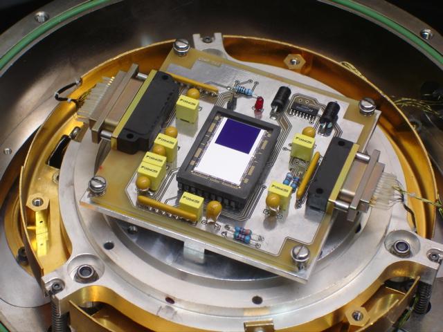
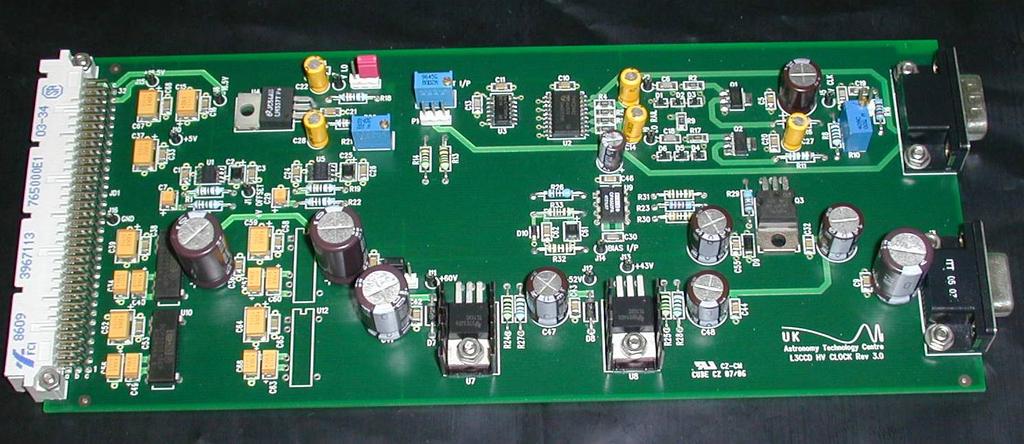
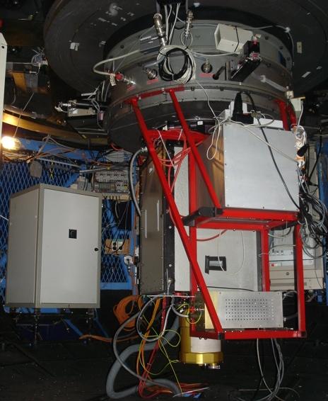
14 ULTRASPEC ULTRASPEC high speed spectro-photometer camera commissioned on ESO La Silla 3.6 m telescope on EFOSC instrument Based on new Electron Multiplication CCD technology OPTICON funded project to show benefits of this technology Frame transfer architecture also given read out efficiency improvements New high voltage clock board developed for SDSU-III controller 14

15 E2V CCD201 1K Frame Transfer CCD 2-Phase Image / storage registers Two Outputs Conventional output Avalanche output 604 Multiplication elements 15
16 ULTRASPEC High-speed Spectroscopy with zero read noise 16
17 Talk Overview Introduction to L3CCD (EM CCD) ULTRASPEC Performance and Issues New L3 CCD Proposal 17
18 Performance Read Noise Avalanche Output (Avalanche Gain = 1) Normal Output Parameter Slow Speed Fast Speed Slow Speed Fast Speed Gain (e/dn) Read Noise 4.0e 10.2e 10.6e 24.7e Frame time 4.8s 1.7s 9.7s 3.4s Window (Y=100) 0.24s 0.09s 0.46s 0.17s 18
19 Gain Controlled by HV Clock Gain HV Clock High (V) Under software control Possible to have different gain for different parts of the CCD Gain can also be switched off no gain noise 19
20 Gain Varies with Temperature Gain increases at lower temperature due to increased probability of the impact ionisation Lattice vibrations are less at lower temperatures 20
21 Clock Induced Charge Clock induced charge occurs in every CCD Dominated by readout noise in standard CCD S N = S 2 g C 2S R Serial register only Serial and prallel 21
22 Performance - CIC Average CIC in a frame System Sensitivity Avalanche Gain Transimpedance Read Noise Average CIC in a frame = = = = = = ADU ADU/e e/adu e = 2.94 ADU e/pixel/frame 22

23 CIC Simulated Overscan 23


24 L3 Performance Dark Non-inverted operation Inverted operation 24

25 Operating Regimes The three operating modes of an EMCCD, shown in terms of the exposure time required to reach a given signal to noise ratio compared to a perfect shot noise limited detector, all else being equal. 25
26 Photon Counting Photon detection efficiency versus detection threshold Photon detection efficiency vs. threshold % detection of input photo electrons y = 100e -1x No loss in S/N Ideal performance Low CIC Critical threshold Detection threshold (electrons at input to L3 register) Threshold is normally set at 5σ Avalanche gain is set at 10 times of the threshold 26
 Top: 10s Spectrum using avalanche output of the UltraSpec Bottom: 10s of Spectrum using normal output (conventional CCDs) S/N Gain: Factor of three 3.6m Telescope with L3 CCD is equivalent to 6.")
27 Normal vs. Avalanche Outputs L3 Camera commissioned with EFOSC2 at ESO s 3.6m Telescope in La Silla (Dec. 06) Top: 10s Spectrum using avalanche output of the UltraSpec Bottom: 10s of Spectrum using normal output (conventional CCDs) S/N Gain: Factor of three 3.6m Telescope with L3 CCD is equivalent to 6.4m telescope with conventional CCD Dead time negligible with EM CCDs compared to the conventional CCDs ESO Messenger, March 07 27
28 Ageing Effect Drop in multiplication gain over time Shift in the high voltage clock amplitude Ageing time constants Short term Long term Depends on signal size Function of gain 28
29 Talk Overview Introduction to L3CCD (EM CCD) ULTRASPEC Performance and Issues New L3 CCD Proposal 29
30 New L3 CCD Proposal Looking for 1M funding for new EM CCD to cover spatial/spectral range and increased read speeds because of FT architecture ESO agreed to lend the NGC 30
31 Details of Specifications 4096 x 1024 pixels for imaging and likewise for storage 2µm-15µm square pixels, with 100% pixel fill factor. 8 outputs, 3 e rms at 100 khz pixel but can operate at 7.5 MHz. 10 Hz full frame rate. Thinned and back illuminated. E2V Technologies Astro broadband AR coating. 2 phase vertical clocking. A minimum of Grade 1 cosmetic quality. Flatness better than 15 µm peak to valley across full length of detector. Reference/dark rows, columns and blank elements to be supplied on the CCD. Each of output to have separate Output Drain (OD) and Reset Drain (RD) pins. 31
32 Efficiency of the New Design Observing speed improvement for L3CCD against standard CCD (3e rms read noise) versus photon rate Observing speed factor improvement 100 SN=5 with EM 10 SN=10 with EM SN=25 with EM SN=50 with EM SN=100 with EM SN=200 with EM SN=5, FT, no EM SN=10, FT, no EM 1 SN=25, FT, no EM SN=50, FT, no EM SN=100, FT, no EM SN=200, FT, no EM 0.1 electrons/pixel/second
33 Thank You 33
ULTRASPEC An Electron Multiplication CCD camera for very low light level high speed astronomical spectrometry
 ULTRASPEC An Electron Multiplication CCD camera for very low light level high speed astronomical spectrometry Derek Ives *a, Nagaraja Bezawada a, Vik Dhillon b, Tom Marsh c a UK Astronomy Technology Centre,
Electron Multiplying Charge Coupled Devices. Craig Mackay, Institute of Astronomy, University of Cambridge.
 Electron Multiplying Charge Coupled Devices Craig Mackay, Institute of Astronomy, University of Cambridge. Outline Introduction to EMCCDs: General Characteristics Applications of EMCCDs: Current and Potential
AstraLux SNR and DR considerations
 AstraLux SNR page 1 AstraLux SNR and DR considerations Stefan Hippler, hippler@mpia.de, March 2008 AstraLux Homepage: http://www.mpia.de/astralux Contents 1 Signal to Noise (SNR) considerations for AstraLux
THE CCD RIDDLE REVISTED: SIGNAL VERSUS TIME LINEAR SIGNAL VERSUS VARIANCE NON-LINEAR
 THE CCD RIDDLE REVISTED: SIGNAL VERSUS TIME LINEAR SIGNAL VERSUS VARIANCE NON-LINEAR Mark Downing 1, Peter Sinclaire 1. 1 ESO, Karl Schwartzschild Strasse-2, 85748 Munich, Germany. ABSTRACT The photon
CCD97-00 Back Illuminated 2-Phase IMO Series Electron Multiplying CCD Sensor
 CCD97-00 Back Illuminated 2-Phase IMO Series Electron Multiplying CCD Sensor INTRODUCTION The CCD97 is part of the L3Vision TM range of products from e2v technologies. This device uses a novel output amplifier
CCDS. Lesson I. Wednesday, August 29, 12
 CCDS Lesson I CCD OPERATION The predecessor of the CCD was a device called the BUCKET BRIGADE DEVICE developed at the Phillips Research Labs The BBD was an analog delay line, made up of capacitors such
the need for an intensifier
 * The LLLCCD : Low Light Imaging without the need for an intensifier Paul Jerram, Peter Pool, Ray Bell, David Burt, Steve Bowring, Simon Spencer, Mike Hazelwood, Ian Moody, Neil Catlett, Philip Heyes Marconi
E2V Technologies CCD42-80 Back Illuminated High Performance CCD Sensor
 E2V Technologies CCD42-80 Back Illuminated High Performance CCD Sensor FEATURES * 2048 by 4096 Pixel Format * 1.5 mm Square Pixels * Image Area 27.6 x 55. mm * Wide Dynamic Range * Symmetrical Anti-static
CCD42-40 NIMO Back Illuminated High Performance CCD Sensor
 CCD42-40 NIMO Back Illuminated High Performance CCD Sensor FEATURES 2048 by 2048 pixel format 13.5 mm square pixels Image area 27.6 x 27.6 mm Back Illuminated format for high quantum efficiency Full-frame
CCD42-10 Back Illuminated High Performance AIMO CCD Sensor
 CCD42-10 Back Illuminated High Performance AIMO CCD Sensor FEATURES 2048 by 512 pixel format 13.5 µm square pixels Image area 27.6 x 6.9 mm Wide Dynamic Range Symmetrical anti-static gate protection Back
CCD30 11 Back Illuminated High Performance CCD Sensor
 CCD30 11 Back Illuminated High Performance CCD Sensor FEATURES * 1024 by 256 Pixel Format * 26 mm Square Pixels * Image Area 26.6 x 6.7 mm * Wide Dynamic Range * Symmetrical Anti-static Gate Protection
CCD Back Illuminated 2-Phase IMO Series Electron Multiplying CCD Sensor
 CCD201-20 Back Illuminated 2-Phase IMO Series Electron Multiplying CCD Sensor INTRODUCTION The CCD201 is a large format sensor (41k 2 ) in the L3Vision TM range of products from e2v technologies. This
CCD42-80 Back Illuminated High Performance CCD Sensor
 CCD42-80 Back Illuminated High Performance CCD Sensor FEATURES * 2048 by 4096 Pixel Format * 13.5 mm Square Pixels * Image Area 27.6 x 55.3 mm * Wide Dynamic Range * Symmetrical Anti-static Gate Protection
CCD47-10 NIMO Back Illuminated Compact Pack High Performance CCD Sensor
 CCD47-10 NIMO Back Illuminated Compact Pack High Performance CCD Sensor FEATURES 1024 by 1024 Nominal (1056 by 1027 Usable Pixels) Image area 13.3 x 13.3mm Back Illuminated format for high quantum efficiency
Electron Multiplying CCDs
 SNIC Symposium, Stanford, California 3-6 April 2006 Electron Multiplying CCDs P.A.Jerram, P. J. Pool, D. J. Burt, R. T. Bell, M.S.Robbins e2v technologies ltd, 106, Waterhouse Lane, Chelmsford, Essex,
Optical/IR Observational Astronomy Detectors II. David Buckley, SAAO
 David Buckley, SAAO 1 The Next Revolution: Charge Couple Device Detectors (CCDs) 2 Optical/IR Observational Astronomy CCDs Integrated semi-conductor detector From photon detection (pair production) to
CCD47-20 Back Illuminated NIMO High Performance NIMO Back Illuminated CCD Sensor
 CCD47-20 Back Illuminated NIMO High Performance NIMO Back Illuminated CCD Sensor FEATURES * 1024 by 1024 1:1 Image Format * Image Area 13.3 x 13.3 mm * Back Illuminated Format * Frame Transfer Operation
E2V Technologies CCD42-10 Inverted Mode Sensor High Performance AIMO CCD Sensor
 E2V Technologies CCD42-1 Inverted Mode Sensor High Performance AIMO CCD Sensor FEATURES * 248 by 512 Pixel Format * 13.5 mm Square Pixels * Image Area 27.6 x 6.9 mm * Wide Dynamic Range * Symmetrical Anti-static
An Introduction to CCDs. The basic principles of CCD Imaging is explained.
 An Introduction to CCDs. The basic principles of CCD Imaging is explained. Morning Brain Teaser What is a CCD? Charge Coupled Devices (CCDs), invented in the 1970s as memory devices. They improved the
CCD67 Back Illuminated AIMO High Performance Compact Pack CCD Sensor
 CCD67 Back Illuminated AIMO High Performance Compact Pack CCD Sensor FEATURES * 256 x 256 Pixel Image Area. * 26 mm Square Pixels. * Low Noise, High Responsivity Output Amplifier. * 1% Active Area. * Gated
MAIN FEATURES OVERVIEW GENERAL DATA ORDERING INFORMATION
 CCD201-20 Datasheet Electron Multiplying CCD Sensor Back Illuminated, 1024 x 1024 Pixels 2-Phase IMO MAIN FEATURES 1024 x 1024 active pixels 13µm square pixels Variable multiplicative gain Additional conventional
CCD97 00 Front Illuminated 2-Phase IMO Series Electron Multiplying CCD Sensor
 CCD97 00 Front Illuminated 2-Phase IMO Series Electron Multiplying CCD Sensor INTRODUCTION The CCD97 is part of the new L3Vision 2 range of products from e2v technologies. This device uses a novel output
Introduction to CCD camera
 Observational Astronomy 2011/2012 Introduction to CCD camera Charge Coupled Device (CCD) photo sensor coupled to shift register Jörg R. Hörandel Radboud University Nijmegen http://particle.astro.ru.nl/goto.html?astropract1-1112
Olivier Daigle a,b, Claude Carignan a, Sébastien Blais-Ouellette b
 Faint flux performance of an EMCCD Olivier Daigle a,b, Claude Carignan a, Sébastien Blais-Ouellette b a Laboratoire d Astrophysique Expérimentale, Département de physique, Université de Montréal, C.P.
TAOS II: Three 88-Megapixel astronomy arrays of large area, backthinned, and low-noise CMOS sensors
 TAOS II: Three 88-Megapixel astronomy arrays of large area, backthinned, and low-noise CMOS sensors CMOS Image Sensors for High Performance Applications TOULOUSE WORKSHOP - 26th & 27th NOVEMBER 2013 Jérôme
CCD42-40 NIMO Back Illuminated High Performance CCD Sensor
 CCD4240 NIMO Back Illuminated High Performance CCD Sensor FEATURES 2048 by 2048 pixel format 13.5 mm square pixels Image area 27.6 x 27.6 mm Back Illuminated format for high quantum efficiency Fullframe
BASLER A601f / A602f
 Camera Specification BASLER A61f / A6f Measurement protocol using the EMVA Standard 188 3rd November 6 All values are typical and are subject to change without prior notice. CONTENTS Contents 1 Overview
Detectors for microscopy - CCDs, APDs and PMTs. Antonia Göhler. Nov 2014
 Detectors for microscopy - CCDs, APDs and PMTs Antonia Göhler Nov 2014 Detectors/Sensors in general are devices that detect events or changes in quantities (intensities) and provide a corresponding output,
ING Technical Note 132
 ING Technical Note 132 Simon Tulloch Department of Physics & Astronomy The University of Sheffield October 25th 2010 1 Contents 1 Introduction 4 2 Key EMCCD concepts 4 2.1 EMCCD structure..................................
Camera Test Protocol. Introduction TABLE OF CONTENTS. Camera Test Protocol Technical Note Technical Note
 Technical Note CMOS, EMCCD AND CCD CAMERAS FOR LIFE SCIENCES Camera Test Protocol Introduction The detector is one of the most important components of any microscope system. Accurate detector readings
CCD55-30 Inverted Mode Sensor High Performance CCD Sensor
 CCD55-3 Inverted Mode Sensor High Performance CCD Sensor FEATURES * 1252 (H) by 1152 (V) Pixel Format * 28 by 26 mm Active Area * Visible Light and X-Ray Sensitive * New Improved Very Low Noise Amplifier
Marconi Applied Technologies CCD39-01 Back Illuminated High Performance CCD Sensor
 Marconi Applied Technologies CCD39-01 Back Illuminated High Performance CCD Sensor FEATURES * 80 by 80 1:1 Image Format * Image Area 1.92 x 1.92 mm * Split-frame Transfer Operation * 24 mm Square Pixels
The Charge-Coupled Device. Many overheads courtesy of Simon Tulloch
 The Charge-Coupled Device Astronomy 1263 Many overheads courtesy of Simon Tulloch smt@ing.iac.es Jan 24, 2013 What does a CCD Look Like? The fine surface electrode structure of a thick CCD is clearly visible
Marconi Applied Technologies CCD30-11 Inverted Mode Sensor High Performance CCD Sensor
 Marconi Applied Technologies CCD30-11 Inverted Mode Sensor High Performance CCD Sensor FEATURES * 1024 by 256 Pixel Format * 26 mm Square Pixels * Image Area 26.6 x 6.7 mm * Wide Dynamic Range * Symmetrical
Last class. This class. CCDs Fancy CCDs. Camera specs scmos
 CCDs and scmos Last class CCDs Fancy CCDs This class Camera specs scmos Fancy CCD cameras: -Back thinned -> higher QE -Unexposed chip -> frame transfer -Electron multiplying -> higher SNR -Fancy ADC ->
CCD42-40 Ceramic AIMO Back Illuminated Compact Package High Performance CCD Sensor
 CCD42-40 Ceramic AIMO Back Illuminated Compact Package High Performance CCD Sensor FEATURES * 2048 by 2048 pixel format * 1.5 mm square pixels * Image area 27.6 x 27.6 mm * Back Illuminated format for
Marconi Applied Technologies CCD47-20 High Performance CCD Sensor
 Marconi Applied Technologies CCD47-20 High Performance CCD Sensor FEATURES * 1024 by 1024 1:1 Image Format * Image Area 13.3 x 13.3 mm * Frame Transfer Operation * 13 mm Square Pixels * Symmetrical Anti-static
Charged-Coupled Devices
 Charged-Coupled Devices Charged-Coupled Devices Useful texts: Handbook of CCD Astronomy Steve Howell- Chapters 2, 3, 4.4 Measuring the Universe George Rieke - 3.1-3.3, 3.6 CCDs CCDs were invented in 1969
Light gathering Power: Magnification with eyepiece:
 Telescopes Light gathering Power: The amount of light that can be gathered by a telescope in a given amount of time: t 1 /t 2 = (D 2 /D 1 ) 2 The larger the diameter the smaller the amount of time. If
Properties of a Detector
 Properties of a Detector Quantum Efficiency fraction of photons detected wavelength and spatially dependent Dynamic Range difference between lowest and highest measurable flux Linearity detection rate
Padova and Asiago Observatories
 ISSN 1594-1906 Padova and Asiago Observatories The Echelle E2V CCD47-10 CCD H. Navasardyan, M. D'Alessandro, E. Giro, Technical Report n. 22 September 2004 Document available at: http://www.pd.astro.it/
Requirements for high-speed spectroscopy using L3CCDs
 Requirements for high-speed spectroscopy using L3CCDs 1 Introduction Vik Dhillon & Tom Marsh, 10 February 2006 This document describes the functional and performance requirements for a high-speed spectroscopic
High-Speed, Photon Counting CCD Cameras for Astronomy
 High-Speed, Photon Counting CCD Cameras for Astronomy Craig Mackay a, *, Tim D. Staley a, David King a, Frank Suess a and Keith Weller a a Institute of Astronomy, University of Cambridge, Madingley Road,
CCD30-11 NIMO Back Illuminated Deep Depleted High Performance CCD Sensor
 CCD30-11 NIMO Back Illuminated Deep Depleted High Performance CCD Sensor FEATURES 1024 by 256 Pixel Format 26µm Square Pixels Image area 26.6 x 6.7mm Back Illuminated format for high quantum efficiency
Where detectors are used in science & technology
 Lecture 9 Outline Role of detectors Photomultiplier tubes (photoemission) Modulation transfer function Photoconductive detector physics Detector architecture Where detectors are used in science & technology
STA1600LN x Element Image Area CCD Image Sensor
 ST600LN 10560 x 10560 Element Image Area CCD Image Sensor FEATURES 10560 x 10560 Photosite Full Frame CCD Array 9 m x 9 m Pixel 95.04mm x 95.04mm Image Area 100% Fill Factor Readout Noise 2e- at 50kHz
An Introduction to Scientific Imaging C h a r g e - C o u p l e d D e v i c e s
 p a g e 2 S C I E N T I F I C I M A G I N G T E C H N O L O G I E S, I N C. Introduction to the CCD F u n d a m e n t a l s The CCD Imaging A r r a y An Introduction to Scientific Imaging C h a r g e -
CCD30-11 Front Illuminated Advanced Inverted Mode High Performance CCD Sensor
 CCD30-11 Front Illuminated Advanced Inverted Mode High Performance CCD Sensor FEATURES 1024 by 256 Pixel Format 26 µm Square Pixels Image Area 26.6 x 6.7 mm Wide Dynamic Range Symmetrical Anti-static Gate
DU-897 (back illuminated)
") IMAGING Andor s ixon EM + DU-897 back illuminated EMCCD has single photon detection capability without an image intensifier, combined with greater than 90% QE of a back-illuminated sensor. Containing a
IMAGING Andor s ixon EM + DU-897 back illuminated EMCCD has single photon detection capability without an image intensifier, combined with greater than 90% QE of a back-illuminated sensor. Containing a
CCD77-00 Front Illuminated High Performance IMO Device
 CCD77- Front Illuminated High Performance IMO Device FEATURES * 512 by 512 Image Format * Image Area 12.3 x 12.3 mm * Full-Frame Operation * 24 mm Square Pixels * Low Noise Output Amplifiers * 1% Active
Detailed Characterisation of a New Large Area CCD Manufactured on High Resistivity Silicon
 Detailed Characterisation of a New Large Area CCD Manufactured on High Resistivity Silicon Mark S. Robbins *, Pritesh Mistry, Paul R. Jorden e2v technologies Ltd, 106 Waterhouse Lane, Chelmsford, Essex
Single Photon Counting in the Visible
 Single Photon Counting in the Visible OUTLINE System Definition DePMOS and RNDR Device Concept RNDR working principle Experimental results Gatable APS devices Achieved and achievable performance Conclusions
Infrared detectors for wavefront sensing
 Infrared detectors for wavefront sensing Jean-Luc Gach et al. The project has received funding from the European Union's Horizon 2020 research and innovation programme under grant agreement No 673944 First
Astronomical Imaging With EMCCDs Using Long Exposures
 Astronomical Imaging With EMCCDs Using Long Exposures Olivier Daigle a, Oleg Djazovski b, Jean Dupuis b, René Doyon c, and Étienne Artigau c a Nüvü Camēras, 5155 Decelles Avenue, Pavillon JA Bombardier,
CCD reductions techniques
 CCD reductions techniques Origin of noise Noise: whatever phenomena that increase the uncertainty or error of a signal Origin of noises: 1. Poisson fluctuation in counting photons (shot noise) 2. Pixel-pixel
CCD Procurement Specification EUV Imaging Spectrometer
 Solar-B EIS * CCD Procurement Specification EUV Imaging Spectrometer Title CCD Procurement specification Doc ID MSSL/SLB-EIS/SP/02 ver 2.0 Author Chris McFee Date 25 March 2001 Ver 2.0 Page 2 of 10 Contents
CCD Characteristics Lab
 CCD Characteristics Lab Observational Astronomy 6/6/07 1 Introduction In this laboratory exercise, you will be using the Hirsch Observatory s CCD camera, a Santa Barbara Instruments Group (SBIG) ST-8E.
STA3600A 2064 x 2064 Element Image Area CCD Image Sensor
 ST600A 2064 x 2064 Element Image Area CCD Image Sensor FEATURES 2064 x 2064 CCD Image Array 15 m x 15 m Pixel 30.96 mm x 30.96 mm Image Area Near 100% Fill Factor Readout Noise Less Than 3 Electrons at
EM-CCD Technical Note (Dec./2009)
") R EM-CCD CAMERA C90-13, -14 EM-CCD Technical Note (Dec./2009) 1. CCD Structures and Characteristics 1.1 Interline Transfer CCD (IL-CCD) 1.2 Full Frame (FFT-CCD) and Frame Transfer CCD (FT-CCD) 1.3 Back-Thinned
R EM-CCD CAMERA C90-13, -14 EM-CCD Technical Note (Dec./2009) 1. CCD Structures and Characteristics 1.1 Interline Transfer CCD (IL-CCD) 1.2 Full Frame (FFT-CCD) and Frame Transfer CCD (FT-CCD) 1.3 Back-Thinned
DV420 SPECTROSCOPY. issue 2 rev 1 page 1 of 5m. associated with LN2
 SPECTROSCOPY Andor s DV420 CCD cameras offer the best price/performance for a wide range of spectroscopy applications. The 1024 x 256 array with 26µm 2 pixels offers the best dynamic range versus resolution.
Low noise readout techniques for Charge Coupled Devices (CCD) Gustavo Cancelo, Juan Estrada, Guillermo Fernandez Moroni, Ken Treptow, Ted Zmuda
 Gustavo Cancelo, Juan Estrada, Guillermo Fernandez Moroni, Ken Treptow, Ted Zmuda") Low noise readout techniques for Charge Coupled Devices (CCD) Gustavo Cancelo, Juan Estrada, Guillermo Fernandez Moroni, Ken Treptow, Ted Zmuda Charge Coupled Devices (CCD) Potential well Characteristics:
Low noise readout techniques for Charge Coupled Devices (CCD) Gustavo Cancelo, Juan Estrada, Guillermo Fernandez Moroni, Ken Treptow, Ted Zmuda Charge Coupled Devices (CCD) Potential well Characteristics:
CCD42-90 Back Illuminated High Performance CCD Sensor
 CCD42-90 Back Illuminated High Performance CCD Sensor FEATURES * 2048 by 4608 Pixel Format * 1.5 mm Square Pixels * Image Area 27.6 x 62.2 mm * Back Illuminated Format for High Quantum Efficiency * Low
Backgrounds in DMTPC. Thomas Caldwell. Massachusetts Institute of Technology DMTPC Collaboration
 Backgrounds in DMTPC Thomas Caldwell Massachusetts Institute of Technology DMTPC Collaboration Cygnus 2009 June 12, 2009 Outline Expected backgrounds for surface run Detector operation Characteristics
Characterisation of a CMOS Charge Transfer Device for TDI Imaging
 Preprint typeset in JINST style - HYPER VERSION Characterisation of a CMOS Charge Transfer Device for TDI Imaging J. Rushton a, A. Holland a, K. Stefanov a and F. Mayer b a Centre for Electronic Imaging,
Basler aca640-90gm. Camera Specification. Measurement protocol using the EMVA Standard 1288 Document Number: BD Version: 02
 Basler aca64-9gm Camera Specification Measurement protocol using the EMVA Standard 1288 Document Number: BD584 Version: 2 For customers in the U.S.A. This equipment has been tested and found to comply
Electron-Multiplying (EM) Gain 2006, 2007 QImaging. All rights reserved.
 Gain 2006, 2007 QImaging. All rights reserved.") D IGITAL IMAGING made easy TECHNICAL NOTE Electron-Multiplying (EM) Gain 26, 27 QImaging. All rights reserved. In order to gain a clearer understanding of biological processes at the single-molecule level,
D IGITAL IMAGING made easy TECHNICAL NOTE Electron-Multiplying (EM) Gain 26, 27 QImaging. All rights reserved. In order to gain a clearer understanding of biological processes at the single-molecule level,
Single Electron per Pixel Counting with Fully Depleted Charge Coupled Devices
 Single Electron per Pixel Counting with Fully Depleted Charge Coupled Devices Miguel Sofo Haro 1,2,3 1 Instituto Balseiro, Universidad Nacional de Cuyo, Argentina. 2 Consejo Nacional de Investigaciones
Electron-Bombarded CMOS
 New Megapixel Single Photon Position Sensitive HPD: Electron-Bombarded CMOS University of Lyon / CNRS-IN2P3 in collaboration with J. Baudot, E. Chabanat, P. Depasse, W. Dulinski, N. Estre, M. Winter N56:
Low light electron multiplying image sensors modeling and characterization : Study of the EMCMOS concept. Timothée Brugière
 Low light electron multiplying image sensors modeling and characterization : Study of the EMCMOS concept Timothée Brugière NDP 2014-30 juin 2014 Groupe ebcmos Why low ux? 2/13 Fast detection Acquisition
CCD44-82 Back Illuminated High Performance CCD Sensor
 CCD44-82 Back Illuminated High Performance CCD Sensor FEATURES * 2048 by 4096 Pixel Format * 15.0 mm Square Pixels * Image Area 30.7 x 61.4 mm * Back Illuminated Format for High Quantum Efficiency * Low
MAOP-702. CCD 47 Characterization
 Doc # : MAOP702 Date: 2013Apr03 Page: 1 of 14 MAOP702 Prepared By: Name(s) and Signature(s) Date Jared R. Males Approved By Name and Signature Title Laird Close PI Victor Gasho Program Manager Date Revision
Photons and solid state detection
 Photons and solid state detection Photons represent discrete packets ( quanta ) of optical energy Energy is hc/! (h: Planck s constant, c: speed of light,! : wavelength) For solid state detection, photons
CCD Analogy BUCKETS (PIXELS) HORIZONTAL CONVEYOR BELT (SERIAL REGISTER) VERTICAL CONVEYOR BELTS (CCD COLUMNS) RAIN (PHOTONS)
 HORIZONTAL CONVEYOR BELT (SERIAL REGISTER) VERTICAL CONVEYOR BELTS (CCD COLUMNS) RAIN (PHOTONS)") CCD Analogy RAIN (PHOTONS) VERTICAL CONVEYOR BELTS (CCD COLUMNS) BUCKETS (PIXELS) HORIZONTAL CONVEYOR BELT (SERIAL REGISTER) MEASURING CYLINDER (OUTPUT AMPLIFIER) Exposure finished, buckets now contain
CCD Analogy RAIN (PHOTONS) VERTICAL CONVEYOR BELTS (CCD COLUMNS) BUCKETS (PIXELS) HORIZONTAL CONVEYOR BELT (SERIAL REGISTER) MEASURING CYLINDER (OUTPUT AMPLIFIER) Exposure finished, buckets now contain
The DSI for Autostar Suite
 An Introduction To DSI Imaging John E. Hoot President Software Systems Consulting 1 The DSI for Autostar Suite Meade Autostar Suite Not Just A Project, A Mission John E. Hoot System Architect 2 1 DSI -
Astronomy 341 Fall 2012 Observational Astronomy Haverford College. CCD Terminology
 CCD Terminology Read noise An unavoidable pixel-to-pixel fluctuation in the number of electrons per pixel that occurs during chip readout. Typical values for read noise are ~ 10 or fewer electrons per
X-ray Spectroscopy Laboratory Suresh Sivanandam Dunlap Institute for Astronomy & Astrophysics, University of Toronto
 X-ray Spectroscopy Laboratory Suresh Sivanandam, 1 Introduction & Objectives At X-ray, ultraviolet, optical and infrared wavelengths most astronomical instruments employ the photoelectric effect to convert
*Sub-Electron Read Noise at MHz Pixel Rates
 *Sub-Electron Read Noise at MHz Pixel Rates Craig D. Mackay, Robert N. Tubbs, Institute of Astronomy, University of Cambridge, Madingley Road, Cambridge, CB3 0HA, UK Ray Bell, David Burt, Paul Jerram,
PIXIS-XO: 1024B 1024 x 1024 imaging array 13 x 13 µm pixels
 The PIXIS-XO series of fully integrated imaging cameras utilizes back-illuminated (BI) and back-illuminated, deepdepletion CCDs without AR coating, for direct detection of the widest range of X-rays between
Southern African Large Telescope SALTICAM Preliminary Design Review. Document Number 3360AE0001: Detector Document
 3360AE0001: Detector Document 1 Southern African Large Telescope SALTICAM Preliminary Design Review Document Number 3360AE0001: Detector Document Darragh O Donoghue Dave Carter Geoff Evans Willie Koorts
Charge coupled devices at ESO - Performances and results
 Charge coupled devices at ESO - Performances and results Cyril Cavadore and Reinhold J. Dorn and James W. Beletic European Southern Observatory, Germany Abstract: The Optical Detector Team at the European
Cerro Tololo Inter-American Observatory. CHIRON manual. A. Tokovinin Version 2. May 25, 2011 (manual.pdf)
") Cerro Tololo Inter-American Observatory CHIRON manual A. Tokovinin Version 2. May 25, 2011 (manual.pdf) 1 1 Overview Calibration lamps Quartz, Th Ar Fiber Prism Starlight GAM mirror Fiber Viewer FEM Guider
Cerro Tololo Inter-American Observatory CHIRON manual A. Tokovinin Version 2. May 25, 2011 (manual.pdf) 1 1 Overview Calibration lamps Quartz, Th Ar Fiber Prism Starlight GAM mirror Fiber Viewer FEM Guider
PIXIS-XO: 400B 1340 x 400 imaging array 20 x 20 µm pixels Direct detection
 PIXIS-XO: 400B 1340 x 400 imaging array 20 x 20 µm pixels Direct detection The PIXIS-XO series of fully integrated imaging cameras utilizes back-illuminated (BI) and back-illuminated, deepdepletion (BR)
Basler aca gm. Camera Specification. Measurement protocol using the EMVA Standard 1288 Document Number: BD Version: 01
 Basler aca5-14gm Camera Specification Measurement protocol using the EMVA Standard 188 Document Number: BD563 Version: 1 For customers in the U.S.A. This equipment has been tested and found to comply with
Upgrade to Andor s high-resolution Luca EM R EMCCD; the new price/performance benchmark.
 Features & benefits EMCCD Technology Ultimate in sensitivity from EMCCD gain. Even single photons are amplified above the noise. Full QE of the sensor is harnessed (visit www.emccd.com) Megapixel sensor
IV DETECTORS. Daguerrotype of the Moon, John W. Draper. March 26, 1840 New York
 IV DETECTORS Lit.: C.R.Kitchin: Astrophysical Techniques, 2009 C.D.Mckay: CCD s in Astronomy, Ann.Rev. A.&A. 24, 1986 G.H.Rieke: Infrared Detector Arrays for Astronomy, Ann.Rev. A&A 45, 2007 up to 1837:
PIXIS-XO: 1024B 1024 x 1024 imaging array 13 x 13 µm pixels
 The PIXIS-XO series of fully integrated imaging cameras utilizes back-illuminated and back-illuminated deep depletion CCDs without AR coating, for direct detection of the widest range of X-rays between
Abstract. Preface. Acknowledgments
 Contents Abstract Preface Acknowledgments iv v vii 1 Introduction 1 1.1 A Very Brief History of Visible Detectors in Astronomy................ 1 1.2 The CCD: Astronomy s Champion Workhorse......................
CCDs for Earth Observation James Endicott 1 st September th UK China Workshop on Space Science and Technology, Milton Keynes, UK
 CCDs for Earth Observation James Endicott 1 st September 2011 7 th UK China Workshop on Space Science and Technology, Milton Keynes, UK Introduction What is this talk all about? e2v sensors in spectrometers
PRELIMINARY. CCD 3041 Back-Illuminated 2K x 2K Full Frame CCD Image Sensor FEATURES
 CCD 3041 Back-Illuminated 2K x 2K Full Frame CCD Image Sensor FEATURES 2048 x 2048 Full Frame CCD 15 µm x 15 µm Pixel 30.72 mm x 30.72 mm Image Area 100% Fill Factor Back Illuminated Multi-Pinned Phase
CCD1600A Full Frame CCD Image Sensor x Element Image Area
 - 1 - General Description CCD1600A Full Frame CCD Image Sensor 10560 x 10560 Element Image Area General Description The CCD1600 is a 10560 x 10560 image element solid state Charge Coupled Device (CCD)
NGC user report. Gert Finger
 NGC user report Gert Finger Overview user s perspective of the transition from IRACE to NGC Performance of NGC prototypes with optical and infrared detectors Implementation of two special features on the
CCD Back Illuminated Scientific CCD Sensor 2048 x 2048 Pixels, Four Outputs and Inverted Mode Operation
 CCD230-42 Back Illuminated Scientific CCD Sensor 2048 x 2048 Pixels, Four Outputs and Inverted Mode Operation INTRODUCTION This device extends e2v s family of scientific CCD sensors. The CCD230 has been
AST Lab exercise: CCD
 AST2210 - Lab exercise: CCD 1 Introduction In this project we will study the performance of a standard CCD, similar to those used in astronomical observations. In particular, the exercise will take you
Description of the UCam detector control system with a particular emphasis to a development of 4Kx4K camera systems
 Description of the UCam detector control system with a particular emphasis to a development of 4Kx4K camera systems Nagaraja Bezawada* a, Stewart McLay a and Derek Ives b a UK Astronomy Technology Centre,
A large format, high-performance CCD sensor for medical x-ray applications
 A large format, high-performance CCD sensor for medical x-ray applications William Des Jardin, Chris Parks, Hung Doan, Neal Kurfiss, and Keith Wetzel Eastman Kodak Company, Rochester, NY, 14650-2008 USA
Basler aca km. Camera Specification. Measurement protocol using the EMVA Standard 1288 Document Number: BD Version: 03
 Basler aca-18km Camera Specification Measurement protocol using the EMVA Standard 188 Document Number: BD59 Version: 3 For customers in the U.S.A. This equipment has been tested and found to comply with
Optional AR coating and wedge windows are available
 TThe PIXIS series from Princeton Instruments (PI) are fully integrated, low noise cameras designed for quantitative scientific imaging optical spectroscopy applications. Designed utilizing PI s exclusive
IR Detectors Developments for Space Applications
 CMOS Image Sensors for High Performance Applications Toulouse, France, 6 th & 7 th December 2011 IR Detectors Developments for Space Applications Harald Weller SELEX GALILEO Infrared Ltd, Southampton,
Silicon sensors for radiant signals. D.Sc. Mikko A. Juntunen
 Silicon sensors for radiant signals D.Sc. Mikko A. Juntunen 2017 01 16 Today s outline Introduction Basic physical principles PN junction revisited Applications Light Ionizing radiation X-Ray sensors in
Pixel Response Effects on CCD Camera Gain Calibration
 1 of 7 1/21/2014 3:03 PM HO M E P R O D UC T S B R IE F S T E C H NO T E S S UP P O RT P UR C HA S E NE W S W E B T O O L S INF O C O NTA C T Pixel Response Effects on CCD Camera Gain Calibration Copyright