TAOS II: Three 88-Megapixel astronomy arrays of large area, backthinned, and low-noise CMOS sensors
|
|
|
- Theodora Green
- 6 years ago
- Views:
Transcription
 Shiang-Yu Wang and Matt Lehner (ASIAA) John Geary (Harvard Smithsonian Center for")
1 TAOS II: Three 88-Megapixel astronomy arrays of large area, backthinned, and low-noise CMOS sensors CMOS Image Sensors for High Performance Applications TOULOUSE WORKSHOP - 26th & 27th NOVEMBER 2013 Jérôme Pratlong, Bruno Gilli, Steve Bowring, Paul Jerram, Paul Jorden, Paul Trinder and Andrew Payne (e2v) Shiang-Yu Wang and Matt Lehner (ASIAA) John Geary (Harvard Smithsonian Center for Astrophysics)
2 NAS

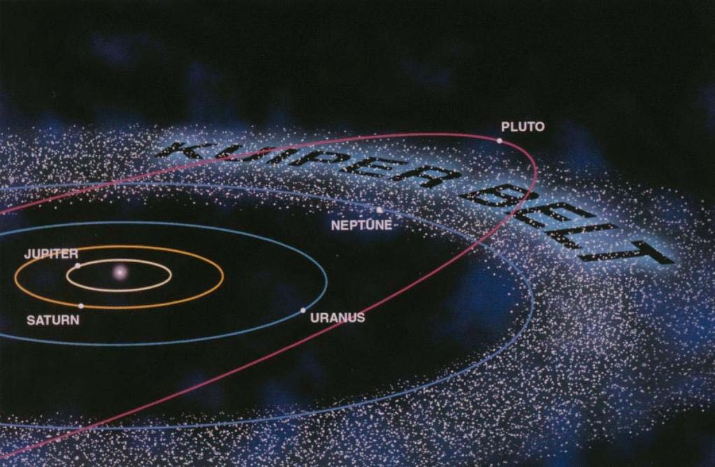
3 TNOs smaller than 20Km diameter can t be directly detected by any telescope Occultation is the only way to detect them

4 Diffraction of Occultation The period for the occultation is about 0.2s. Better resolution in time can provide more information for the size and distance of the objects. TAOS2 sampling is 20Hz
 Readout the area with stars only 1000 stars in each chip 6x6 pixels per star @20Hz <100KHz CMOS sensor EM CCD generates more noise for bright objects and requires good gain control.")
5 Plausible Options Readout at 20MHz but with low noise Typical rate ~ few Ke 2e read noise can be achieved by amplifying the signal before readout Electron multiplication CCD (EM or L3 CCD) Readout the area with stars only 1000 stars in each chip 6x6 pixels per <100KHz CMOS sensor EM CCD generates more noise for bright objects and requires good gain control.
6 CMOS sensor needs Format : 4608 x 1920 (16µm pixel pitch) Pixel size : 10~16 microns QE : > 80% from 500~750nm Read noise : < 5e Full well : > 10000e Window switching time : < 0.5ms Total pixel rate : > 16Mpixel/s Dark rate : < 1e /s
7 Challenges CMOS detector design: Flexible access for windowing Large buttable device using stitching technology Low noise Astronomy detector therefore needs: Flatness of the packaging Backthinned High red QE Cryogenic cooling Slide 7
8 TAOSII detector: Architecture overview Focal plane using 10 image sensors of 1920 x 4608 size butted 16 µm square pixel pitch Array composed of 8 segments for parallel read-out Pixel array access by half row (left and right) independently ROI mode to speed up frame rate Multi-ROI mode access (both directions column and row) to concentrate on different area of the pixel array. Noise floor below 5e - RMS and low dark current. Slide 8
9 TAOSII detector: Architecture details 6 dummy rows Stitched block decoder Row decoder Row buffer 6 dummcolumns ioutput 1920 X 4608 Useful pixel (12x11 Dummy pixels 1 test line) 6 dummcolumns Row buffer Row decoder Stitched block decoder 5 dummy rows + 1 test line Read out path Global analogue bias Column decoder Serial column interface Serial row interface Output buffer Test block Serial row interface Pad Ring Slide 9
10 TAOSII detector: Generic access Option to acquire the next row while reading out the previous one. Slide 10
11 TAOSII detector: Readoutpath allowing acquisition of a row while reading Slide 11
12 TAOSII detector: row and column access Serial data in col_ser<7:0> col_clk col_load Column decoder approach by loading the address in a register first before sending the information to the local column decoder via a second register. Same concept used for row access. row_ser_in_l/r row_clk_l/r 13 bits register Pixel array The row address is sent to a register and when ready released to the local row decoder. row_load_l/r Row register 13 bits Row decoder This implementation does not any additional pin than a scan approach. A segment B segment Slide 12
13 TAOSII technology: Overview Tower have overcome potential lag effect. Photodiode - PPD Transfer gate STI PDP PD STI Dedicated light N-implant PWELL PDN PWELL Ground potential V PINNED P-Sub VSWING Reset potential Technology: 5T pinned photodiode pixel for low noise and anti-blooming feature 1-D Stitching Backthinned imager for high QE at high wavelength Epi starting material 18µm thinned down to 9µm (will be adjusted for best MTF) High resistance material 1Kohm.cm-1 Two layers ARC for high QE over the range of 500nm to 750nm Operational temperature between -40oC and possibly -100oC Slide 13
14 TAOSII Pixel: 5T approach Vrefr max about 2.8V Dark level 2.6V after feedthrough. 5 th transistor is working in anti-blooming With 0V on the gate. The 5 th transistor is driven by a logic signal: If programmed to 0V then it is an anti-blooming If programmed to toggle from 0V to supply then it acts as a global reset. Item Description TRANSISTORS M SF Nmos Source Follower amplifier transistor: low noise process. M SEL Nmos select transistor: low noise process. M TRA Nmos transfer transistor. M RST Nmos reset transistor: low noise process Nmos global reset transistor or Nmos anti-blooming transistor. Parasitic conversion capacitance SIGNALS sn Internal to the pixel sense node name sel Select command that connects to the gate of the transistor M SEL. tra Transfer command that connects to the gate of the transistor M TRA. rst Reset command that connects to the gate of the transistor M RST. g_rst Global reset command that connects to the gate of the transistor M G_RST. col Column connection output of the pixel. It is a common signal to all pixel from that column. vrefr Reset voltage level that is applied to the sense node prior to charge transfer. This supply is global to the array. vpix Source follower supply. This supply is global to the array. asub Substrate connection to minimise substrate effect due to the high resistivity material (1kOhm.cm -1 ) used. M G_RST C CONV Slide 14

15 TAOSII Pixel: Layout implementation This pixel is laid out that it is easily sizeable to 12µm pitch. Slide 15

16 Sensor organization Sensor organization as a function of the Stitch plan Segment A contains: Readout Pad ring Column and row registers Column decoders Bottom dummy pixels Segment B is repeated 4 times and contains: Useful pixels 1152 rows per section Column dummy pixels Row decoder and buffer Segment C contains: Top dummy pixels Seal ring Slide 16
17 TAOSII package: 3 sides buttable package Package non-sensitive area Sensor non-sensitive area 50µm 450µm ZIF socket interface (8x10 or 9x9) IMAGE SENSOR Readout area (non-sensitive are IMAGE SENSOR Sensitive area Sensor non-sensitive area 30.7mm 31.6mm Sensor non-sensitive area Package non-sensitive area 450µm 50µm 73.7mm Package 50µm ~76.3±0.3mm 200µm 50µm Requirement for the package: 3 sides buttability Flatness: Peak-to-Valley better than 30µm Value Focal plane sensitive area only 22626mm 2 Focal plane total image area 23818mm 2 Ratio between non-sensitive area and sensitive area Equivalent Fill Factor at focal plane 94% level. Slide 17
 Provision for Temperature Sensor (Not Shown) Stainless Steel Screws & Invar 36 washers Ceramic PGA Slide")
18 TAOSII Backthinned design packaging with 89 pins CMOS Device Invar 36 Package Invar 36 Shims (3 off) Spare Shim Position, not used 2 off Invar 36 Precision Pins PGA Pins Glue Channel Bond pads & Bond wires connecting device to PGA Invar 36 Shim Studs (3 off) Provision for Temperature Sensor (Not Shown) Stainless Steel Screws & Invar 36 washers Ceramic PGA Slide 18
19 TAOSII: Performance Parameter Description Typical estimated performance Units Pixel pitch 16 x16 µm Wavelength application 800 nm FF_BI Back Illuminated Fill Factor in Pixel > 87 % QE Quantum > 60 % Q LIN Linear charge capacity. 15 ke - Q SAT Saturation charge capacity: dominated by 22 ke - the conversion node and not the Pinned Photodiode. CVF Conversion Gain Factor at the output of 75 µv/e - the sensor Lag Residual charge after transfer from the 1 % pinned photodiode to the conversion node. RON Read Out Noise 3 e - RMS DC Dark o C e-/pixel/s MOVS Maximum Output Voltage Swing: 1.8 V Reset level Saturation level. FSR Full Scale Range: output Voltage Swing 1.2 V within linearity level. DR Dynamic range over FSR 74 db Detector will be cooled low enough (about -40oC or below) to meet the 1e-/pixel/s requirement. Non Linearity Error Non Linearity from 5% to 90% of FSR. +/-1 to +/-2 % MTF Modulation transfer 48 % Slide 19
20 TAOSII detector: Flexibility in format BASELINE OPTIONS 4608 X X X X µm pixel pitch: 16µm pixel pitch: 16µm pixel pitch: 16µm pixel pitch: ~ 76.5mm X 31.6mm ~ 58mm X 31.6mm ~ 39.6mm X 31.6mm ~ 21mm X 31.6mm 12µm pixel pitch: 12µm pixel pitch: 12µm pixel pitch: 12µm pixel pitch: ~ 57.5mm X 23.5mm ~ 43.6mm X 23.5mm ~ 30.0mm X 23.5mm ~ 16.0mm X 23.5mm Slide 20
21 TAOSII: Planning 27 th November 2013 Mid-December 2013 Tape-out End March 2014 Wafers at e2v End July 2014 end characterisation Slide 21
22 TAOSII: e2v back face QE measurements on CIS107-4T - 7µm pixel pitch QE Plot at 20 C ) 100% 90% 80% 70% 60% 50% 40% 30% 20% QE Astrium % 0% Wavelength (nm) NB this data is for a two layer AR coating. The model and the measured results are in good agreement indicating that all or nearly all of the generated electrons are gathered by the photodiode. QE is >80% from 450 to 750nm Slide 22

23 TAOSII: Etalon effect front face and back face comparison measured on CIS107 CIS107 4T pixel 7µm pixel pitch FrontFace QE CIS107 4T pixel 7µm pixel pitch BackFace QE Slide 23


24 TAOSII: e2v MTF measurement on high resistivity material CIS107 Thinned to 11µm with a depletion of about 7µm to 8µm. Thinned to 7µm with a depletion of about 1µm to 2µm.. On TAOSII the target will be to thinned between 9µm to 11µm. Experiment might be done to optimise this parameter versus QE Slide 24
25 Conclusion In order to meet the TAOSII image sensor requirements a CMOS detector has been chosen specified with an high level of flexibility leading to the following features: Pixel: 5T technology with a pixel pitch of 16µm. Noise floor aimed at 3e - RMS and 74dB dynamic range (in rolling shutter only) Cryogenic dark current < 1e-/pixel/s (on-going activity at e2v to test similar pixel down to -80oC) 8 each or 16MHz in total with possibility to extend each output to 7MHz. Region of interest and Multi-ROI available in both directions. Possibility to jump in both directions. Row access by half of the row: left half and right half independent access. Read while acquiring pixel of the next row. High frame rate, combining pixel acquisition while reading and ROI/JUMP, down to 6µs. Rolling shutter and electronic global shutter modes available. Anti-blooming built-in. Solution stitch-able 1D. The first results are expected by end summer Slide 25

26 Acknowledgements Special Thanks Shiang-Yu Wang from ASIAA Matt Lehner from ASIAA John Geary from Harvard Smithsonian Center for Astrophysics e2v co-writers and reviewers Slide 26
Low temperature measurements of the large-area, backthinned, and lownoise TAOSII CMOS sensors
 Low temperature measurements of the large-area, backthinned, and lownoise TAOSII CMOS sensors Steven Johnson, Jérôme Pratlong, Amr Ibrahim, Paul Jerram, Paul Jorden (e2v technologies) Shiang-Yu Wang and
Characteristic of e2v CMOS Sensors for Astronomical Applications
 Characteristic of e2v CMOS Sensors for Astronomical Applications Shiang-Yu Wang* a, Hung-Hsu Ling a, Yen-Sang Hu a, John C. Geary b, Stephen M. Amato b, Jerome Pratlong c, Andrew Pike c, Paul Jorden c
EVALUATION OF RADIATION HARDNESS DESIGN TECHNIQUES TO IMPROVE RADIATION TOLERANCE FOR CMOS IMAGE SENSORS DEDICATED TO SPACE APPLICATIONS
 EVALUATION OF RADIATION HARDNESS DESIGN TECHNIQUES TO IMPROVE RADIATION TOLERANCE FOR CMOS IMAGE SENSORS DEDICATED TO SPACE APPLICATIONS P. MARTIN-GONTHIER, F. CORBIERE, N. HUGER, M. ESTRIBEAU, C. ENGEL,
CMOS sensor for TAOS 2
 CMOS sensor for TAOS 2 Shiang-Yu Wang ( 王祥宇 ) Academia Sinica, Institute of Astronomy & Astrophysics Taiwan American Occultation Survey Institute of Astronomy & Astrophysics, Academia Sinica, Taiwan Sun-Kun
Laboratory, University of Arizona, Tucson, AZ 85721; c ImagerLabs, 1995 S. Myrtle Ave., Monrovia CA INTRODUCTION ABSTRACT
 A CMOS Visible Image Sensor with Non-Destructive Readout Capability Gary R. Sims* a, Gene Atlas c, Eric Christensen b, Roger W. Cover a, Stephen Larson b, Hans J. Meyer a, William V. Schempp a a Spectral
Jan Bogaerts imec
 imec 2007 1 Radiometric Performance Enhancement of APS 3 rd Microelectronic Presentation Days, Estec, March 7-8, 2007 Outline Introduction Backside illuminated APS detector Approach CMOS APS (readout)
E2V Technologies CCD42-80 Back Illuminated High Performance CCD Sensor
 E2V Technologies CCD42-80 Back Illuminated High Performance CCD Sensor FEATURES * 2048 by 4096 Pixel Format * 1.5 mm Square Pixels * Image Area 27.6 x 55. mm * Wide Dynamic Range * Symmetrical Anti-static
Design and Performance of a Pinned Photodiode CMOS Image Sensor Using Reverse Substrate Bias
 Design and Performance of a Pinned Photodiode CMOS Image Sensor Using Reverse Substrate Bias 13 September 2017 Konstantin Stefanov Contents Background Goals and objectives Overview of the work carried
A 1Mjot 1040fps 0.22e-rms Stacked BSI Quanta Image Sensor with Cluster-Parallel Readout
 A 1Mjot 1040fps 0.22e-rms Stacked BSI Quanta Image Sensor with Cluster-Parallel Readout IISW 2017 Hiroshima, Japan Saleh Masoodian, Jiaju Ma, Dakota Starkey, Yuichiro Yamashita, Eric R. Fossum May 2017
CCD42-80 Back Illuminated High Performance CCD Sensor
 CCD42-80 Back Illuminated High Performance CCD Sensor FEATURES * 2048 by 4096 Pixel Format * 13.5 mm Square Pixels * Image Area 27.6 x 55.3 mm * Wide Dynamic Range * Symmetrical Anti-static Gate Protection
More Imaging Luc De Mey - CEO - CMOSIS SA
 More Imaging Luc De Mey - CEO - CMOSIS SA Annual Review / June 28, 2011 More Imaging CMOSIS: Vision & Mission CMOSIS s Business Concept On-Going R&D: More Imaging CMOSIS s Vision Image capture is a key
European Low Flux CMOS Image Sensor
 European Low Flux CMOS Image Sensor Description and Preliminary Results Ajit Kumar Kalgi 1, Wei Wang 1, Bart Dierickx 1, Dirk Van Aken 1, Kaiyuan Wu 1, Alexander Klekachev 1, Gerlinde Ruttens 1, Kyriaki
Light gathering Power: Magnification with eyepiece:
 Telescopes Light gathering Power: The amount of light that can be gathered by a telescope in a given amount of time: t 1 /t 2 = (D 2 /D 1 ) 2 The larger the diameter the smaller the amount of time. If
2 nd Generation CMOS Charge Transfer TDI: Results on Proton Irradiation
 2 nd Generation CMOS Charge Transfer TDI: Results on Proton Irradiation F. Mayer, J. Endicott, F. Devriere e2v, Avenue de Rochepleine, BP123, 38521 Saint Egrève Cedex, France J. Rushton, K. Stefanov, A.
Marconi Applied Technologies CCD39-01 Back Illuminated High Performance CCD Sensor
 Marconi Applied Technologies CCD39-01 Back Illuminated High Performance CCD Sensor FEATURES * 80 by 80 1:1 Image Format * Image Area 1.92 x 1.92 mm * Split-frame Transfer Operation * 24 mm Square Pixels
Detailed Characterisation of a New Large Area CCD Manufactured on High Resistivity Silicon
 Detailed Characterisation of a New Large Area CCD Manufactured on High Resistivity Silicon Mark S. Robbins *, Pritesh Mistry, Paul R. Jorden e2v technologies Ltd, 106 Waterhouse Lane, Chelmsford, Essex
Fully depleted, thick, monolithic CMOS pixels with high quantum efficiency
 Fully depleted, thick, monolithic CMOS pixels with high quantum efficiency Andrew Clarke a*, Konstantin Stefanov a, Nicholas Johnston a and Andrew Holland a a Centre for Electronic Imaging, The Open University,
CCDs for Earth Observation James Endicott 1 st September th UK China Workshop on Space Science and Technology, Milton Keynes, UK
 CCDs for Earth Observation James Endicott 1 st September 2011 7 th UK China Workshop on Space Science and Technology, Milton Keynes, UK Introduction What is this talk all about? e2v sensors in spectrometers
CMOS Today & Tomorrow
 CMOS Today & Tomorrow Uwe Pulsfort TDALSA Product & Application Support Overview Image Sensor Technology Today Typical Architectures Pixel, ADCs & Data Path Image Quality Image Sensor Technology Tomorrow
Marconi Applied Technologies CCD47-20 High Performance CCD Sensor
 Marconi Applied Technologies CCD47-20 High Performance CCD Sensor FEATURES * 1024 by 1024 1:1 Image Format * Image Area 13.3 x 13.3 mm * Frame Transfer Operation * 13 mm Square Pixels * Symmetrical Anti-static
TDI-CMOS Image Sensor for Earth Observation
 TDI-CMOS Image Sensor for Earth Observation Jérôme Pratlong *a, Paul Jerram a, Georgios Tsiolis a, Vincent Arkesteijn b ; Paul Donegan c ; Laurens Korthout d a Teledyne-e2v, Waterhouse Lane, Chelmsford,
High QE, Thinned Backside-Illuminated, 3e- RoN, Fast 700fps, 1760x1760 Pixels Wave-Front Sensor Imager with Highly Parallel Readout
 High QE, Thinned Backside-Illuminated, 3e- RoN, Fast 700fps, 1760x1760 Pixels Wave-Front Sensor Imager with Highly Parallel Readout Mark Downing, Dietrich Baade, Norbert Hubin, Olaf Iwert, Javier Reyes
CCD55-30 Inverted Mode Sensor High Performance CCD Sensor
 CCD55-3 Inverted Mode Sensor High Performance CCD Sensor FEATURES * 1252 (H) by 1152 (V) Pixel Format * 28 by 26 mm Active Area * Visible Light and X-Ray Sensitive * New Improved Very Low Noise Amplifier
Simulation of High Resistivity (CMOS) Pixels
 Pixels") Simulation of High Resistivity (CMOS) Pixels Stefan Lauxtermann, Kadri Vural Sensor Creations Inc. AIDA-2020 CMOS Simulation Workshop May 13 th 2016 OUTLINE 1. Definition of High Resistivity Pixel Also
Simulation of High Resistivity (CMOS) Pixels Stefan Lauxtermann, Kadri Vural Sensor Creations Inc. AIDA-2020 CMOS Simulation Workshop May 13 th 2016 OUTLINE 1. Definition of High Resistivity Pixel Also
CCD and CMOS Imaging Devices for Large (Ground Based) Telescopes. Veljko Radeka BNL SNIC April 3, 2006
 Telescopes. Veljko Radeka BNL SNIC April 3, 2006") CCD and CMOS Imaging Devices for Large (Ground Based) Telescopes Veljko Radeka BNL SNIC April 3, 2006 1 Large Telescopes Survey telescope Deep probe Primary Mirror dia.=d m, Area= A Large (~8m) Very large
CCD and CMOS Imaging Devices for Large (Ground Based) Telescopes Veljko Radeka BNL SNIC April 3, 2006 1 Large Telescopes Survey telescope Deep probe Primary Mirror dia.=d m, Area= A Large (~8m) Very large
FUTURE PROSPECTS FOR CMOS ACTIVE PIXEL SENSORS
 FUTURE PROSPECTS FOR CMOS ACTIVE PIXEL SENSORS Dr. Eric R. Fossum Jet Propulsion Laboratory Dr. Philip H-S. Wong IBM Research 1995 IEEE Workshop on CCDs and Advanced Image Sensors April 21, 1995 CMOS APS
Low Light Level CCD Performance and Issues
 Low Light Level CCD Performance and Issues Nagaraja Bezawada UK Astronomy Technology Centre 04 July 2007 Overview of the Talk Introduction to L3CCD (EM CCD) ULTRASPEC Performance and Issues New L3 CCD
CCD44-82 Back Illuminated High Performance CCD Sensor
 CCD44-82 Back Illuminated High Performance CCD Sensor FEATURES * 2048 by 4096 Pixel Format * 15.0 mm Square Pixels * Image Area 30.7 x 61.4 mm * Back Illuminated Format for High Quantum Efficiency * Low
CCD42-40 NIMO Back Illuminated High Performance CCD Sensor
 CCD42-40 NIMO Back Illuminated High Performance CCD Sensor FEATURES 2048 by 2048 pixel format 13.5 mm square pixels Image area 27.6 x 27.6 mm Back Illuminated format for high quantum efficiency Full-frame
CCD42-10 Back Illuminated High Performance AIMO CCD Sensor
 CCD42-10 Back Illuminated High Performance AIMO CCD Sensor FEATURES 2048 by 512 pixel format 13.5 µm square pixels Image area 27.6 x 6.9 mm Wide Dynamic Range Symmetrical anti-static gate protection Back
Detectors that cover a dynamic range of more than 1 million in several dimensions
 Detectors that cover a dynamic range of more than 1 million in several dimensions Detectors for Astronomy Workshop Garching, Germany 10 October 2009 James W. Beletic Teledyne Providing the best images
CCD30-11 NIMO Back Illuminated Deep Depleted High Performance CCD Sensor
 CCD30-11 NIMO Back Illuminated Deep Depleted High Performance CCD Sensor FEATURES 1024 by 256 Pixel Format 26µm Square Pixels Image area 26.6 x 6.7mm Back Illuminated format for high quantum efficiency
CCD47-10 NIMO Back Illuminated Compact Pack High Performance CCD Sensor
 CCD47-10 NIMO Back Illuminated Compact Pack High Performance CCD Sensor FEATURES 1024 by 1024 Nominal (1056 by 1027 Usable Pixels) Image area 13.3 x 13.3mm Back Illuminated format for high quantum efficiency
CCD42-90 Back Illuminated High Performance CCD Sensor
 CCD42-90 Back Illuminated High Performance CCD Sensor FEATURES * 2048 by 4608 Pixel Format * 1.5 mm Square Pixels * Image Area 27.6 x 62.2 mm * Back Illuminated Format for High Quantum Efficiency * Low
PRELIMINARY. CCD 3041 Back-Illuminated 2K x 2K Full Frame CCD Image Sensor FEATURES
 CCD 3041 Back-Illuminated 2K x 2K Full Frame CCD Image Sensor FEATURES 2048 x 2048 Full Frame CCD 15 µm x 15 µm Pixel 30.72 mm x 30.72 mm Image Area 100% Fill Factor Back Illuminated Multi-Pinned Phase
CCD30 11 Back Illuminated High Performance CCD Sensor
 CCD30 11 Back Illuminated High Performance CCD Sensor FEATURES * 1024 by 256 Pixel Format * 26 mm Square Pixels * Image Area 26.6 x 6.7 mm * Wide Dynamic Range * Symmetrical Anti-static Gate Protection
E2V Technologies CCD42-10 Inverted Mode Sensor High Performance AIMO CCD Sensor
 E2V Technologies CCD42-1 Inverted Mode Sensor High Performance AIMO CCD Sensor FEATURES * 248 by 512 Pixel Format * 13.5 mm Square Pixels * Image Area 27.6 x 6.9 mm * Wide Dynamic Range * Symmetrical Anti-static
IT FR R TDI CCD Image Sensor
 4k x 4k CCD sensor 4150 User manual v1.0 dtd. August 31, 2015 IT FR 08192 00 R TDI CCD Image Sensor Description: With the IT FR 08192 00 R sensor ANDANTA GmbH builds on and expands its line of proprietary
Marconi Applied Technologies CCD30-11 Inverted Mode Sensor High Performance CCD Sensor
 Marconi Applied Technologies CCD30-11 Inverted Mode Sensor High Performance CCD Sensor FEATURES * 1024 by 256 Pixel Format * 26 mm Square Pixels * Image Area 26.6 x 6.7 mm * Wide Dynamic Range * Symmetrical
DV420 SPECTROSCOPY. issue 2 rev 1 page 1 of 5m. associated with LN2
 SPECTROSCOPY Andor s DV420 CCD cameras offer the best price/performance for a wide range of spectroscopy applications. The 1024 x 256 array with 26µm 2 pixels offers the best dynamic range versus resolution.
Where detectors are used in science & technology
 Lecture 9 Outline Role of detectors Photomultiplier tubes (photoemission) Modulation transfer function Photoconductive detector physics Detector architecture Where detectors are used in science & technology
CCD Back Illuminated 2-Phase IMO Series Electron Multiplying CCD Sensor
 CCD201-20 Back Illuminated 2-Phase IMO Series Electron Multiplying CCD Sensor INTRODUCTION The CCD201 is a large format sensor (41k 2 ) in the L3Vision TM range of products from e2v technologies. This
Fundamentals of CMOS Image Sensors
 CHAPTER 2 Fundamentals of CMOS Image Sensors Mixed-Signal IC Design for Image Sensor 2-1 Outline Photoelectric Effect Photodetectors CMOS Image Sensor(CIS) Array Architecture CIS Peripherals Design Considerations
CCD47-20 Back Illuminated NIMO High Performance NIMO Back Illuminated CCD Sensor
 CCD47-20 Back Illuminated NIMO High Performance NIMO Back Illuminated CCD Sensor FEATURES * 1024 by 1024 1:1 Image Format * Image Area 13.3 x 13.3 mm * Back Illuminated Format * Frame Transfer Operation
STA1600LN x Element Image Area CCD Image Sensor
 ST600LN 10560 x 10560 Element Image Area CCD Image Sensor FEATURES 10560 x 10560 Photosite Full Frame CCD Array 9 m x 9 m Pixel 95.04mm x 95.04mm Image Area 100% Fill Factor Readout Noise 2e- at 50kHz
CCD Scientific CCD Sensor Back Illuminated, 2048 x 4096 Pixels, Non Inverted Mode Operation Enhanced red sensitivity
 CCD261-84 Scientific CCD Sensor Back Illuminated, 2048 x 4096 Pixels, Non Inverted Mode Operation Enhanced red sensitivity INTRODUCTION This device is primarily a full-frame sensor with an image area of
KAF E. 512(H) x 512(V) Pixel. Enhanced Response. Full-Frame CCD Image Sensor. Performance Specification. Eastman Kodak Company
 x 512(V) Pixel. Enhanced Response. Full-Frame CCD Image Sensor. Performance Specification. Eastman Kodak Company") KAF - 0261E 512(H) x 512(V) Pixel Enhanced Response Full-Frame CCD Image Sensor Performance Specification Eastman Kodak Company Image Sensor Solutions Rochester, New York 14650 Revision 2 December 21,
KAF - 0261E 512(H) x 512(V) Pixel Enhanced Response Full-Frame CCD Image Sensor Performance Specification Eastman Kodak Company Image Sensor Solutions Rochester, New York 14650 Revision 2 December 21,
CCD67 Back Illuminated AIMO High Performance Compact Pack CCD Sensor
 CCD67 Back Illuminated AIMO High Performance Compact Pack CCD Sensor FEATURES * 256 x 256 Pixel Image Area. * 26 mm Square Pixels. * Low Noise, High Responsivity Output Amplifier. * 1% Active Area. * Gated
Open Research Online The Open University s repository of research publications and other research outputs
 Open Research Online The Open University s repository of research publications and other research outputs Fully depleted and backside biased monolithic CMOS image sensor Conference or Workshop Item How
Last class. This class. CCDs Fancy CCDs. Camera specs scmos
 CCDs and scmos Last class CCDs Fancy CCDs This class Camera specs scmos Fancy CCD cameras: -Back thinned -> higher QE -Unexposed chip -> frame transfer -Electron multiplying -> higher SNR -Fancy ADC ->
A High Image Quality Fully Integrated CMOS Image Sensor
 A High Image Quality Fully Integrated CMOS Image Sensor Matt Borg, Ray Mentzer and Kalwant Singh Hewlett-Packard Company, Corvallis, Oregon Abstract We describe the feature set and noise characteristics
Ultra-high resolution 14,400 pixel trilinear color image sensor
 Ultra-high resolution 14,400 pixel trilinear color image sensor Thomas Carducci, Antonio Ciccarelli, Brent Kecskemety Microelectronics Technology Division Eastman Kodak Company, Rochester, New York 14650-2008
CCD Scientific Sensor Back Illuminated, 2048 x 4096 Pixels, Non Inverted Mode Operation High-Rho Enhanced Red Sensitivity
 CCD261-84 Scientific Sensor Back Illuminated, 2048 x 4096 Pixels, Non Inverted Mode Operation High-Rho Enhanced Red Sensitivity INTRODUCTION This device is primarily a full-frame sensor with an image area
ABSTRACTT. developments. applications. 1.2 GigaPixel. 2.1 CIS113 (Vega) figures below. illustrate the. another paper. 3. The
 figures below. illustrate the. another paper. 3. The") e2v CCD and CMOS sensors and systems designed for astronomical applications Paul Jorden*, Paul Jerram, J Doug Jordan, Jérôme Pratlong, Markk Robbins e2v technologies, 106 Waterhouse Lane, Chelmsford, Essex,
e2v CCD and CMOS sensors and systems designed for astronomical applications Paul Jorden*, Paul Jerram, J Doug Jordan, Jérôme Pratlong, Markk Robbins e2v technologies, 106 Waterhouse Lane, Chelmsford, Essex,
the need for an intensifier
 * The LLLCCD : Low Light Imaging without the need for an intensifier Paul Jerram, Peter Pool, Ray Bell, David Burt, Steve Bowring, Simon Spencer, Mike Hazelwood, Ian Moody, Neil Catlett, Philip Heyes Marconi
ONE TE C H N O L O G Y PLACE HOMER, NEW YORK TEL: FAX: /
 ONE TE C H N O L O G Y PLACE HOMER, NEW YORK 13077 TEL: +1 607 749 2000 FAX: +1 607 749 3295 www.panavisionimaging.com / sales@panavisionimaging.com High Performance Linear Image Sensors ELIS-1024 IMAGER
High Dynamic Range, PSN Limited, Synchronous Shutter Image sensor
 10 Presented at the Caeleste Visionary Workshop The Future of High-end Image Sensors 06 April 2016 High Dynamic Range, PSN Limited, Synchronous Shutter Image sensor A. Kalgi, B. Luyssaert, B. Dierickx,
pco.edge 4.2 LT 0.8 electrons 2048 x 2048 pixel 40 fps up to :1 up to 82 % pco. low noise high resolution high speed high dynamic range
 edge 4.2 LT scientific CMOS camera high resolution 2048 x 2048 pixel low noise 0.8 electrons USB 3.0 small form factor high dynamic range up to 37 500:1 high speed 40 fps high quantum efficiency up to
CCD30-11 Front Illuminated Advanced Inverted Mode High Performance CCD Sensor
 CCD30-11 Front Illuminated Advanced Inverted Mode High Performance CCD Sensor FEATURES 1024 by 256 Pixel Format 26 µm Square Pixels Image Area 26.6 x 6.7 mm Wide Dynamic Range Symmetrical Anti-static Gate
Characterisation of a CMOS Charge Transfer Device for TDI Imaging
 Preprint typeset in JINST style - HYPER VERSION Characterisation of a CMOS Charge Transfer Device for TDI Imaging J. Rushton a, A. Holland a, K. Stefanov a and F. Mayer b a Centre for Electronic Imaging,
CCD97 00 Front Illuminated 2-Phase IMO Series Electron Multiplying CCD Sensor
 CCD97 00 Front Illuminated 2-Phase IMO Series Electron Multiplying CCD Sensor INTRODUCTION The CCD97 is part of the new L3Vision 2 range of products from e2v technologies. This device uses a novel output
ELEN6350. Summary: High Dynamic Range Photodetector Hassan Eddrees, Matt Bajor
 ELEN6350 High Dynamic Range Photodetector Hassan Eddrees, Matt Bajor Summary: The use of image sensors presents several limitations for visible light spectrometers. Both CCD and CMOS one dimensional imagers
CCD42-40 NIMO Back Illuminated High Performance CCD Sensor
 CCD4240 NIMO Back Illuminated High Performance CCD Sensor FEATURES 2048 by 2048 pixel format 13.5 mm square pixels Image area 27.6 x 27.6 mm Back Illuminated format for high quantum efficiency Fullframe
Based on lectures by Bernhard Brandl
 Astronomische Waarneemtechnieken (Astronomical Observing Techniques) Based on lectures by Bernhard Brandl Lecture 10: Detectors 2 1. CCD Operation 2. CCD Data Reduction 3. CMOS devices 4. IR Arrays 5.
Open Research Online The Open University s repository of research publications and other research outputs
 Open Research Online The Open University s repository of research publications and other research outputs PSF and non-uniformity in a monolithic, fully depleted, 4T CMOS image sensor Conference or Workshop
Multiple shutter mode radiation hard IR detector ROIC
 Multiple shutter mode radiation hard IR detector ROIC A.K.Kalgi 1, B.Dierickx 1, D. Van Aken 1, A. Ciapponi 4, S.Veijalainen 1, K.Liekens 1, W. Verbruggen 1, P. Hargrave 2, R. Sudiwala 2, M. Haiml 3, H.
Low Power Sensor Concepts
 Low Power Sensor Concepts Konstantin Stefanov 11 February 2015 Introduction The Silicon Pixel Tracker (SPT): The main driver is low detector mass Low mass is enabled by low detector power Benefits the
Minimizes reflection losses from UV-IR; Optional AR coatings & wedge windows are available.
 Now Powered by LightField PyLoN:2K 2048 x 512 The PyLoN :2K is a controllerless, cryogenically-cooled CCD camera designed for quantitative scientific spectroscopy applications demanding the highest possible
IRIS3 Visual Monitoring Camera on a chip
 IRIS3 Visual Monitoring Camera on a chip ESTEC contract 13716/99/NL/FM(SC) G.Meynants, J.Bogaerts, W.Ogiers FillFactory, Mechelen (B) T.Cronje, T.Torfs, C.Van Hoof IMEC, Leuven (B) Microelectronics Presentation
Optional AR coating and wedge windows are available
 TThe PIXIS series from Princeton Instruments (PI) are fully integrated, low noise cameras designed for quantitative scientific imaging optical spectroscopy applications. Designed utilizing PI s exclusive
MAIN FEATURES OVERVIEW GENERAL DATA ORDERING INFORMATION
 CCD201-20 Datasheet Electron Multiplying CCD Sensor Back Illuminated, 1024 x 1024 Pixels 2-Phase IMO MAIN FEATURES 1024 x 1024 active pixels 13µm square pixels Variable multiplicative gain Additional conventional
Characterisation of a Novel Reverse-Biased PPD CMOS Image Sensor
 Characterisation of a Novel Reverse-Biased PPD CMOS Image Sensor Konstantin D. Stefanov, Andrew S. Clarke, James Ivory and Andrew D. Holland Centre for Electronic Imaging, The Open University, Walton Hall,
Minimizes reflection losses from UV to IR; No optical losses due to multiple optical surfaces; Optional AR coating and wedge windows available.
 SOPHIA: 2048B The SOPHIA : 2048B camera from Princeton Instruments (PI) is fully integrated, ultra-low noise 2048 x 2048, 15 µm pixel CCD camera designed expressly for the most demanding quantitative scientific
CCD42-40 Ceramic AIMO Back Illuminated Compact Package High Performance CCD Sensor
 CCD42-40 Ceramic AIMO Back Illuminated Compact Package High Performance CCD Sensor FEATURES * 2048 by 2048 pixel format * 1.5 mm square pixels * Image area 27.6 x 27.6 mm * Back Illuminated format for
CCD77-00 Front Illuminated High Performance IMO Device
 CCD77- Front Illuminated High Performance IMO Device FEATURES * 512 by 512 Image Format * Image Area 12.3 x 12.3 mm * Full-Frame Operation * 24 mm Square Pixels * Low Noise Output Amplifiers * 1% Active
ACTIVE PIXEL SENSORS VS. CHARGE-COUPLED DEVICES
 ACTIVE PIXEL SENSORS VS. CHARGE-COUPLED DEVICES Dr. Eric R. Fossum Imaging Systems Section Jet Propulsion Laboratory, California Institute of Technology (818) 354-3128 1993 IEEE Workshop on CCDs and Advanced
Multi-bit Quanta Image Sensors
 Multi-bit Quanta Image Sensors Eric R. Fossum International Image Sensor Workshop (IISW) Vaals, Netherlands June 10, 2015-1- Quanta Image Sensor Count Every Photoelectron Single-Bit QIS Jot = specialized
A 120dB dynamic range image sensor with single readout using in pixel HDR
 A 120dB dynamic range image sensor with single readout using in pixel HDR CMOS Image Sensors for High Performance Applications Workshop November 19, 2015 J. Caranana, P. Monsinjon, J. Michelot, C. Bouvier,
Active Pixel Sensors Fabricated in a Standard 0.18 um CMOS Technology
 Active Pixel Sensors Fabricated in a Standard.18 um CMOS Technology Hui Tian, Xinqiao Liu, SukHwan Lim, Stuart Kleinfelder, and Abbas El Gamal Information Systems Laboratory, Stanford University Stanford,
Charge coupled CMOS and hybrid detector arrays
 Charge coupled CMOS and hybrid detector arrays James Janesick Sarnoff Corporation, 4952 Warner Ave., Suite 300, Huntington Beach, CA. 92649 Headquarters: CN5300, 201 Washington Road Princeton, NJ 08543-5300
Specifications Summary 1. Array Size (pixels) Pixel Size. Sensor Size. Pixel Well Depth (typical) 95,000 e - 89,000 e -
 Pixel Size. Sensor Size. Pixel Well Depth (typical) 95,000 e - 89,000 e -") Apogee Alta Series System Features 1 High Resolution Sensor 1.0 Megapixel sensor with 13 mm pixels delivers a large field of view with high resolution. Programmable TE cooling down to 50 o C below ambient
Apogee Alta Series System Features 1 High Resolution Sensor 1.0 Megapixel sensor with 13 mm pixels delivers a large field of view with high resolution. Programmable TE cooling down to 50 o C below ambient
FEATURES GENERAL DESCRIPTION. CCD Element Linear Image Sensor CCD Element Linear Image Sensor
 CCD 191 6000 Element Linear Image Sensor FEATURES 6000 x 1 photosite array 10µm x 10µm photosites on 10µm pitch Anti-blooming and integration control Enhanced spectral response (particularly in the blue
CCD525 Time Delay Integration Line Scan Sensor
 CCD525 Time Delay Integration Line Scan Sensor FEATURES 248 Active Pixels Per Line 96 TDI Lines 13µm x13 µm Pixels 4 Speed Output Ports TDI Stages Selectable Between 96, 64, 48, 32, or 24 1 MHz Data Rate
CCD97-00 Back Illuminated 2-Phase IMO Series Electron Multiplying CCD Sensor
 CCD97-00 Back Illuminated 2-Phase IMO Series Electron Multiplying CCD Sensor INTRODUCTION The CCD97 is part of the L3Vision TM range of products from e2v technologies. This device uses a novel output amplifier
The Charge-Coupled Device. Many overheads courtesy of Simon Tulloch
 The Charge-Coupled Device Astronomy 1263 Many overheads courtesy of Simon Tulloch smt@ing.iac.es Jan 24, 2013 What does a CCD Look Like? The fine surface electrode structure of a thick CCD is clearly visible
A new Photon Counting Detector: Intensified CMOS- APS
 A new Photon Counting Detector: Intensified CMOS- APS M. Belluso 1, G. Bonanno 1, A. Calì 1, A. Carbone 3, R. Cosentino 1, A. Modica 4, S. Scuderi 1, C. Timpanaro 1, M. Uslenghi 2 1- I.N.A.F.-Osservatorio
MAPS-based ECAL Option for ILC
 MAPS-based ECAL Option for ILC, Spain Konstantin Stefanov On behalf of J. Crooks, P. Dauncey, A.-M. Magnan, Y. Mikami, R. Turchetta, M. Tyndel, G. Villani, N. Watson, J. Wilson v Introduction v ECAL with
An Introduction to CCDs. The basic principles of CCD Imaging is explained.
 An Introduction to CCDs. The basic principles of CCD Imaging is explained. Morning Brain Teaser What is a CCD? Charge Coupled Devices (CCDs), invented in the 1970s as memory devices. They improved the
DU-897 (back illuminated)
") IMAGING Andor s ixon EM + DU-897 back illuminated EMCCD has single photon detection capability without an image intensifier, combined with greater than 90% QE of a back-illuminated sensor. Containing a
IMAGING Andor s ixon EM + DU-897 back illuminated EMCCD has single photon detection capability without an image intensifier, combined with greater than 90% QE of a back-illuminated sensor. Containing a
A scientific HDR Multi-spectral imaging platform. B. Dupont, Pyxalis, France.
 A scientific HDR Multi-spectral imaging platform B. Dupont, Pyxalis, France. OUTLINE HDPYX HDR Scientific Sensor platform First usage as hyperspectral device by Resolution Spectra and CSUG Perspectives
Photons and solid state detection
 Photons and solid state detection Photons represent discrete packets ( quanta ) of optical energy Energy is hc/! (h: Planck s constant, c: speed of light,! : wavelength) For solid state detection, photons
Non-linear responsivity characterisation of a CMOS Active Pixel Sensor for high resolution imaging of the Jovian system
 Non-linear responsivity characterisation of a CMOS Active Pixel Sensor for high resolution imaging of the Jovian system Matthew Soman, a,* Konstantin Stefanov, a Daniel Weatherill, a Andrew Holland, a
A flexible compact readout circuit for SPAD arrays ABSTRACT Keywords: 1. INTRODUCTION 2. THE SPAD 2.1 Operation 7780C - 55
 A flexible compact readout circuit for SPAD arrays Danial Chitnis * and Steve Collins Department of Engineering Science University of Oxford Oxford England OX13PJ ABSTRACT A compact readout circuit that
CCD1600A Full Frame CCD Image Sensor x Element Image Area
 - 1 - General Description CCD1600A Full Frame CCD Image Sensor 10560 x 10560 Element Image Area General Description The CCD1600 is a 10560 x 10560 image element solid state Charge Coupled Device (CCD)
Single Photon Counting in the Visible
 Single Photon Counting in the Visible OUTLINE System Definition DePMOS and RNDR Device Concept RNDR working principle Experimental results Gatable APS devices Achieved and achievable performance Conclusions
High SEE Tolerance in a Radiation Hardened CMOS Image Sensor Designed for the Meteosat Third Generation FCI-VisDA Instrument
 CMOS Image Sensors for High Performance Applications 18 th and 19 th Nov 2015 High SEE Tolerance in a Radiation Hardened CMOS Image Sensor Designed for the Meteosat Third Generation FCI-VisDA Instrument
Demonstration of a Frequency-Demodulation CMOS Image Sensor
 Demonstration of a Frequency-Demodulation CMOS Image Sensor Koji Yamamoto, Keiichiro Kagawa, Jun Ohta, Masahiro Nunoshita Graduate School of Materials Science, Nara Institute of Science and Technology
Introduction. Chapter 1
 1 Chapter 1 Introduction During the last decade, imaging with semiconductor devices has been continuously replacing conventional photography in many areas. Among all the image sensors, the charge-coupled-device
High-end CMOS Active Pixel Sensor for Hyperspectral Imaging
 R11 High-end CMOS Active Pixel Sensor for Hyperspectral Imaging J. Bogaerts (1), B. Dierickx (1), P. De Moor (2), D. Sabuncuoglu Tezcan (2), K. De Munck (2), C. Van Hoof (2) (1) Cypress FillFactory, Schaliënhoevedreef
A new Photon Counting Detector: Intensified CMOS- APS
 A new Photon Counting Detector: Intensified CMOS- APS M. Belluso 1, G. Bonanno 1, A. Calì 1, A. Carbone 3, R. Cosentino 1, A. Modica 4, S. Scuderi 1, C. Timpanaro 1, M. Uslenghi 2 1-I.N.A.F.-Osservatorio