Photons and solid state detection
|
|
|
- Toby Austin
- 5 years ago
- Views:
Transcription
1 Photons and solid state detection Photons represent discrete packets ( quanta ) of optical energy Energy is hc/! (h: Planck s constant, c: speed of light,! : wavelength) For solid state detection, photons are converted to electrons Electrons can be measured as a current (flow through resistor) or as a voltage (accumulation in capacitor) Detection can be done at a single point (point = small area over which all detected photons are summed up) e.g. photodiode, photomultiplier tubes (PMT) Multiple point detectors can be arrayed to detect an image eg. complementary metal oxide semiconductor (CMOS) or charge coupled device (CCD) sensors. Recall shot noise: photon production is inherently noisy with a standard deviation proportional to the square root of intensity
2 Quantum efficiency and spectral sensitivity Photodiode responsivities. Quantum efficiency = number of electrons generated / incident photon Measured as a unit less fraction or in ampere/watt (called responsivity) QE and responsivity vary with the wavelength of light
3 Photoelectric effect Valence band (VB) is the energy band with bound electrons Conduction band (CB) is the energy band with free electrons Difference is the energy band gap Photoelectric effect describes how electrons can be kicked out of the valence band on supplying energy E g will move electrons to the CB. Eventually they will fall back Ionization energy (IE) will eject an electron from the material. This electron is lost
 above the previous one The electric field between dynodes accelerates electrons as they strike subsequent dynodes Secondary emission causes more electrons to be emitted")
4 Photomultiplier Tube Photoelectric effect dictates ejection of an electron from the photocathode Photoelectrons focused and made to strike an electrode (called dynode) Each dynode is at a +ve potential (10s-100s volts) above the previous one The electric field between dynodes accelerates electrons as they strike subsequent dynodes Secondary emission causes more electrons to be emitted than the number that struck a dynode causing a multiplicative gain (up to 10 8 ) The anode collects all electrons and leads to a current
5 Photodiode pn junction Pure semiconductor is an insulator but can be doped to p type (fixed negative charges, free holes) or n type (fixed positive charges, free electrons) A hole is not a real thing, it is the lack of an electron A depletion region forms with no free charges. There exists an electric field across this region. Region can be expanded by reverse biasing (n region voltage>p region voltage by a few volts)

6 Photodiode operation Photoelectric effect dictates generation of an electron-hole pair (EHP) In the p or the n region the EHP disappears due to recombination In or near the depletion region, the photogenerated free carriers come under the influence of the electric field and causes a current The fact that useful EHP are generated only in a specific region plays a role in determining QE and spectral sensitivity Photocurrent is linearly proportional to the optical power incident
7 Dark current and read noise Dark current is the output of a photodetector is the absence of any light. It is not a constant offset that can be rejected but is also noisy Caused by thermal vibrations leading to EHP creation (PD) or electron ejection (PMT) Limits the lowest light levels that can be detected Read noise is the excess electrical noise (apart from photon shot noise) that appears at the output of a photodetector Independent of optical power, so dominates at low light intensities Dark current (and dark current noise) and read noise can be reduced by cooling the detector
8 Charge coupled device imager Photoelectrons collected in potential wells A well is created if the gate voltage is high By using a cyclic sequence of voltages the collected photoelectrons are moved
9 Charge coupled device imager Photoelectrons of each pixel are moved horizontally (within the same row) into a series of output wells The charge is then transferred vertically A charge-to-voltage amplifier converts the photoelectron charge into a voltage Key ideas The readout is serial While the array is being read, it MUST be protected from light Charge Transfer Efficiency is a critical parameter and measures how much chargeislostpertransfer.itisdefinedas: (charge after transfer)/(charge before transfer)
10 Complementary metal oxide semiconductor imager Column selection Passive pixel array Any pixel can be connected to the charge-to-voltage amplifier using a row and column select mechanism Row selection Switches implemented using MOS transistors Because of the long metal lines between the pixels and the amplifier, this does not work very well Charge to voltage amplifier Output
11 Complementary metal oxide semiconductor imager Column selection Active pixel array Each pixel has its own chargeto-voltage amplifier Row selection Amps and switches implemented by MOS transistors Random access scheme is retained Key feature: processing circuits can be implemented at the pixel or at the column level Key feature: can read one pixel while others are collecting light Output
12 Array imager features Resolution: number of x and y pixels More lead to more detail, but for a given array size more means each pixel is smaller -> smaller photodiode -> poorer sensitivity Pixel pitch: size of one pixel. Down to 1-2 µm using latest fabrication technology Array size (format): size of the array in units of length. Must match image size Fixed pattern noise: spatial noise that is fixed in time. Due to fabrication related differences between individual pixels. Worse in CMOS because each pixel has its own circuitry Fill factor: ratio of area of photodiode to area of pixel Circuits (switches, amps) take up valuable photodiode space Corrective measures Microlenses: per pixel lens increasing light gathering Back-illuminated sensors Frame rate: images per second < 1/(readout time + exposure time) Intensity resolution (how fine a difference) & dynamic range (maximum/minimum)
13 Pixel pitch & sampling requirements Diffraction sets a resolution limit System magnification maps that resolution limit on to an image sensor Pixel pitch needs to be fine enough for adequate sampling Analogous to Nyquist sampling theorem if a signal has a maximum frequency content of B Hz, it must be sampled at > 2B Hz for reconstruction 200 nm apart (object) 20 µm apart (image) 100x magnification Pixel pitch >20 µm >10 µm <10 µm > : just greater than < : just lesser than Pixel pitch at least 2x smaller than optical resolution limit (Rayleigh limit)
14 Digital image representation An image is a two-dimensional array a[x,y] x,y indicate the position of the pixel within an image a[x,y] is the intensity of that pixel. 1 white, 0 black [ 0 1 ] 1 0 For an NxM image x: 1, 2,. N y: 1, 2,. M

15 Digital image representation


16 Spatial resolution Larger pixels lead to lesser detail because a pixel is the smallest unit of an image. It can hold only one intensity.


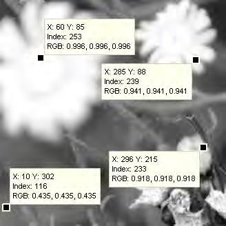
17 Intensity resolution Light intensity is continuous (red), but a digital image can only store discrete values (blue) Due to the binary system used in computers, the number of distinct levels in an N-bit image is 2 N Almost all computer displays are 8-bit which means they can show 256 distinct shades between black (gray level 0) and white (gray level 255) A good imager will have >8 bits, however most common image formats JPG, BMP, PNG are only 8 bit leading to potential loss of information TIFF image format can store up to 16 bits so is preferred Why are more bits useful? 8 bit 4 bit 8 bit 4 bit
18 Saturation and dynamic range Light intensity Saturation level. Any light intensity higher that this can not be differentiated from this level. level 2 N -1 level 2 N -2 level 2 N -3 level 2 level 1 level 0 Digital pixel levels Dynamic range (DR) is the ratio of the maximum to minimum light that can be detected ie (2 N -1)/1 May be smaller due to noise 2 N -1/(noise floor) Usually expressed in decibel (db) 20 log 10 (2 N -1)


19 Color image representation Split into three color channels red, green and blue Each channel can be thought of as a grayscale image

20 Sensing color Sense 1 color channel at a time with a grayscale/monochrome imager and combine images in software. Limitations? Bayer array: color filter array on top of each individual pixel color filters Why twice as many green? Needs interpolation to form image pixels Foveon sensor: uses 3D photodiodes and exploits the dependence of light penetration on wavelength Sensitivity, particularly of deeper structures, suffers blue diode green diode red diode
21 Intensity scaling b For an N-bit imager 255 a! 0 b " 2 N -1 b a >256 levels in image levels for display a <256 levels in image Note <256 levels does not neccesarily indicate <8-bit imager. Consider a 12-bit imager (light dependent levels from 0 to 4095) imaging in very low light. It is possible that the brightest pixel only goes up to <256

22 Contrast Contrast is the percieved difference between various intensity levels in an image Consider the same scene imaged using two cameras. Both have 65 levels. Neither image is scaled Intensity scaling enhances contrast allowing visualization of fine details Given images c, d can you tell which came from which camera? a: Levels 0-64 b: Levels IMPORTANT to be aware of scaling before comparing images c: a scaled to d: b scaled to 0-255
23 Temporal noise and SNR Observe the intensity of 1 particular pixel over multiple images Low noise High noise Both have same mean Pixel level Frame number Multiple images of the same scene Signal to noise ratio = mean(pixel level) / standard deviation(pixel level) SNR (in db) = 20 log 10 (SNR) What happens to SNR with increasing light intensity?
24 Imaging parameters Light available: number of photons available per unit time Exposure time: duration for which photons are collected for 1 image Quantum efficiency: electrons generated per photon Amplifier gain: electron-to-voltage or electron-to-current conversion factor How do we optimise SNR? Maximize collected photons signal # number(photons) shot noise # [number(photons)] 0.5 Minimize read noise
25 Photon Transfer Curve Noise in imagers read noise, shot noise, fixed pattern noise FPN can be eliminated. How? Read noise independent of light intensity Shot noise dependent on light intensity Output signal of imager dependent on light intensity PTC is a log-log plot of signal vs. noise log(noise) Three regions read noise shot noise saturation log(signal)
Engineering Medical Optics BME136/251 Winter 2018
 Engineering Medical Optics BME136/251 Winter 2018 Monday/Wednesday 2:00-3:20 p.m. Beckman Laser Institute Library, MSTB 214 (lab) *1/17 UPDATE Wednesday, 1/17 Optics and Photonic Devices III: homework
Fundamentals of CMOS Image Sensors
 CHAPTER 2 Fundamentals of CMOS Image Sensors Mixed-Signal IC Design for Image Sensor 2-1 Outline Photoelectric Effect Photodetectors CMOS Image Sensor(CIS) Array Architecture CIS Peripherals Design Considerations
Detectors for microscopy - CCDs, APDs and PMTs. Antonia Göhler. Nov 2014
 Detectors for microscopy - CCDs, APDs and PMTs Antonia Göhler Nov 2014 Detectors/Sensors in general are devices that detect events or changes in quantities (intensities) and provide a corresponding output,
EE 392B: Course Introduction
 EE 392B Course Introduction About EE392B Goals Topics Schedule Prerequisites Course Overview Digital Imaging System Image Sensor Architectures Nonidealities and Performance Measures Color Imaging Recent
OPTI510R: Photonics. Khanh Kieu College of Optical Sciences, University of Arizona Meinel building R.626
 OPTI510R: Photonics Khanh Kieu College of Optical Sciences, University of Arizona kkieu@optics.arizona.edu Meinel building R.626 Photodetectors Introduction Most important characteristics Photodetector
An Introduction to CCDs. The basic principles of CCD Imaging is explained.
 An Introduction to CCDs. The basic principles of CCD Imaging is explained. Morning Brain Teaser What is a CCD? Charge Coupled Devices (CCDs), invented in the 1970s as memory devices. They improved the
Ground-based optical auroral measurements
 Ground-based optical auroral measurements FYS 3610 Background Ground-based optical measurements provides a unique way to monitor spatial and temporal variation of auroral activity at high resolution up
Page 1. Ground-based optical auroral measurements. Background. CCD All-sky Camera with filterwheel. Image intensifier
 Ground-based optical auroral measurements FYS 3610 Background Ground-based optical measurements provides a unique way to monitor spatial and temporal variation of auroral activity at high resolution up
Optical Receivers Theory and Operation
 Optical Receivers Theory and Operation Photo Detectors Optical receivers convert optical signal (light) to electrical signal (current/voltage) Hence referred O/E Converter Photodetector is the fundamental
Camera Test Protocol. Introduction TABLE OF CONTENTS. Camera Test Protocol Technical Note Technical Note
 Technical Note CMOS, EMCCD AND CCD CAMERAS FOR LIFE SCIENCES Camera Test Protocol Introduction The detector is one of the most important components of any microscope system. Accurate detector readings
OFCS OPTICAL DETECTORS 11/9/2014 LECTURES 1
 OFCS OPTICAL DETECTORS 11/9/2014 LECTURES 1 1-Defintion & Mechanisms of photodetection It is a device that converts the incident light into electrical current External photoelectric effect: Electrons are
Homework Set 3.5 Sensitive optoelectronic detectors: seeing single photons
 Homework Set 3.5 Sensitive optoelectronic detectors: seeing single photons Due by 12:00 noon (in class) on Tuesday, Nov. 7, 2006. This is another hybrid lab/homework; please see Section 3.4 for what you
DETECTORS Important characteristics: 1) Wavelength response 2) Quantum response how light is detected 3) Sensitivity 4) Frequency of response
 Wavelength response 2) Quantum response how light is detected 3) Sensitivity 4) Frequency of response") DETECTORS Important characteristics: 1) Wavelength response 2) Quantum response how light is detected 3) Sensitivity 4) Frequency of response (response time) 5) Stability 6) Cost 7) convenience Photoelectric
DETECTORS Important characteristics: 1) Wavelength response 2) Quantum response how light is detected 3) Sensitivity 4) Frequency of response (response time) 5) Stability 6) Cost 7) convenience Photoelectric
Charged Coupled Device (CCD) S.Vidhya
 S.Vidhya") Charged Coupled Device (CCD) S.Vidhya 02.04.2016 Sensor Physical phenomenon Sensor Measurement Output A sensor is a device that measures a physical quantity and converts it into a signal which can be read
Charged Coupled Device (CCD) S.Vidhya 02.04.2016 Sensor Physical phenomenon Sensor Measurement Output A sensor is a device that measures a physical quantity and converts it into a signal which can be read
The Charge-Coupled Device. Many overheads courtesy of Simon Tulloch
 The Charge-Coupled Device Astronomy 1263 Many overheads courtesy of Simon Tulloch smt@ing.iac.es Jan 24, 2013 What does a CCD Look Like? The fine surface electrode structure of a thick CCD is clearly visible
Where detectors are used in science & technology
 Lecture 9 Outline Role of detectors Photomultiplier tubes (photoemission) Modulation transfer function Photoconductive detector physics Detector architecture Where detectors are used in science & technology
Silicon sensors for radiant signals. D.Sc. Mikko A. Juntunen
 Silicon sensors for radiant signals D.Sc. Mikko A. Juntunen 2017 01 16 Today s outline Introduction Basic physical principles PN junction revisited Applications Light Ionizing radiation X-Ray sensors in
CHAPTER 9 POSITION SENSITIVE PHOTOMULTIPLIER TUBES
 CHAPTER 9 POSITION SENSITIVE PHOTOMULTIPLIER TUBES The current multiplication mechanism offered by dynodes makes photomultiplier tubes ideal for low-light-level measurement. As explained earlier, there
CCD Characteristics Lab
 CCD Characteristics Lab Observational Astronomy 6/6/07 1 Introduction In this laboratory exercise, you will be using the Hirsch Observatory s CCD camera, a Santa Barbara Instruments Group (SBIG) ST-8E.
Semiconductor Detector Systems
 Semiconductor Detector Systems Helmuth Spieler Physics Division, Lawrence Berkeley National Laboratory OXFORD UNIVERSITY PRESS ix CONTENTS 1 Detector systems overview 1 1.1 Sensor 2 1.2 Preamplifier 3
Image acquisition. In both cases, the digital sensing element is one of the following: Line array Area array. Single sensor
 Image acquisition Digital images are acquired by direct digital acquisition (digital still/video cameras), or scanning material acquired as analog signals (slides, photographs, etc.). In both cases, the
Cameras CS / ECE 181B
 Cameras CS / ECE 181B Image Formation Geometry of image formation (Camera models and calibration) Where? Radiometry of image formation How bright? What color? Examples of cameras What is a Camera? A camera
2013 LMIC Imaging Workshop. Sidney L. Shaw Technical Director. - Light and the Image - Detectors - Signal and Noise
 2013 LMIC Imaging Workshop Sidney L. Shaw Technical Director - Light and the Image - Detectors - Signal and Noise The Anatomy of a Digital Image Representative Intensities Specimen: (molecular distribution)
CCDS. Lesson I. Wednesday, August 29, 12
 CCDS Lesson I CCD OPERATION The predecessor of the CCD was a device called the BUCKET BRIGADE DEVICE developed at the Phillips Research Labs The BBD was an analog delay line, made up of capacitors such
Lecture 8 Optical Sensing. ECE 5900/6900 Fundamentals of Sensor Design
 ECE 5900/6900: Fundamentals of Sensor Design Lecture 8 Optical Sensing 1 Optical Sensing Q: What are we measuring? A: Electromagnetic radiation labeled as Ultraviolet (UV), visible, or near,mid-, far-infrared
Part I. CCD Image Sensors
 Part I CCD Image Sensors 2 Overview of CCD CCD is the abbreviation for charge-coupled device. CCD image sensors are silicon-based integrated circuits (ICs), consisting of a dense matrix of photodiodes
Digital Imaging Rochester Institute of Technology
 Digital Imaging 1999 Rochester Institute of Technology So Far... camera AgX film processing image AgX photographic film captures image formed by the optical elements (lens). Unfortunately, the processing
Characterisation of SiPM Index :
 Characterisation of SiPM --------------------------------------------------------------------------------------------Index : 1. Basics of SiPM* 2. SiPM module 3. Working principle 4. Experimental setup
UNIT VIII-SPECIAL PURPOSE ELECTRONIC DEVICES. 1. Explain tunnel Diode operation with the help of energy band diagrams.
 UNIT III-SPECIAL PURPOSE ELECTRONIC DEICES 1. Explain tunnel Diode operation with the help of energy band diagrams. TUNNEL DIODE: A tunnel diode or Esaki diode is a type of semiconductor diode which is
Components of Optical Instruments
 Components of Optical Instruments General Design of Optical Instruments Sources of Radiation Wavelength Selectors (Filters, Monochromators, Interferometers) Sample Containers Radiation Transducers (Detectors)
Spectroscopy in the UV and Visible: Instrumentation. Spectroscopy in the UV and Visible: Instrumentation
 Spectroscopy in the UV and Visible: Instrumentation Typical UV-VIS instrument 1 Source - Disperser Sample (Blank) Detector Readout Monitor the relative response of the sample signal to the blank Transmittance
Lecture 7. July 24, Detecting light (converting light to electrical signal)
") Lecture 7 July 24, 2017 Detecting light (converting light to electrical signal) Photoconductor Photodiode Managing electrical signal Metal-oxide-semiconductor (MOS) capacitor Charge coupled device (CCD)
Lecture 7 July 24, 2017 Detecting light (converting light to electrical signal) Photoconductor Photodiode Managing electrical signal Metal-oxide-semiconductor (MOS) capacitor Charge coupled device (CCD)
Dynamic Range. Can I look at bright and faint things at the same time?
 Detector Basics The purpose of any detector is to record the light collected by the telescope. All detectors transform the incident radiation into a some other form to create a permanent record, such as
Overview. Charge-coupled Devices. MOS capacitor. Charge-coupled devices. Charge-coupled devices:
 Overview Charge-coupled Devices Charge-coupled devices: MOS capacitors Charge transfer Architectures Color Limitations 1 2 Charge-coupled devices MOS capacitor The most popular image recording technology
Optical Communications
 Optical Communications Telecommunication Engineering School of Engineering University of Rome La Sapienza Rome, Italy 2005-2006 Lecture #4, May 9 2006 Receivers OVERVIEW Photodetector types: Photodiodes
Chap14. Photodiode Detectors
 Chap14. Photodiode Detectors Mohammad Ali Mansouri-Birjandi mansouri@ece.usb.ac.ir mamansouri@yahoo.com Faculty of Electrical and Computer Engineering University of Sistan and Baluchestan (USB) Design
Ultra-high resolution 14,400 pixel trilinear color image sensor
 Ultra-high resolution 14,400 pixel trilinear color image sensor Thomas Carducci, Antonio Ciccarelli, Brent Kecskemety Microelectronics Technology Division Eastman Kodak Company, Rochester, New York 14650-2008
STA1600LN x Element Image Area CCD Image Sensor
 ST600LN 10560 x 10560 Element Image Area CCD Image Sensor FEATURES 10560 x 10560 Photosite Full Frame CCD Array 9 m x 9 m Pixel 95.04mm x 95.04mm Image Area 100% Fill Factor Readout Noise 2e- at 50kHz
Detectors for Optical Communications
 Optical Communications: Circuits, Systems and Devices Chapter 3: Optical Devices for Optical Communications lecturer: Dr. Ali Fotowat Ahmady Sep 2012 Sharif University of Technology 1 Photo All detectors
light sensing & sensors Mo: Tu:04 light sensing & sensors 167+1
 light sensing & sensors 16722 mws@cmu.edu Mo:20090302+Tu:04 light sensing & sensors 167+1 reading Fraden Section 3.13, Light, and Chapter 14, Light Detectors 16722 mws@cmu.edu Mo:20090302+Tu:04 light sensing
Chapter 3 OPTICAL SOURCES AND DETECTORS
 Chapter 3 OPTICAL SOURCES AND DETECTORS 3. Optical sources and Detectors 3.1 Introduction: The success of light wave communications and optical fiber sensors is due to the result of two technological breakthroughs.
Charge-integrating organic heterojunction
 In the format provided by the authors and unedited. DOI: 10.1038/NPHOTON.2017.15 Charge-integrating organic heterojunction Wide phototransistors dynamic range for organic wide-dynamic-range heterojunction
An Introduction to the Silicon Photomultiplier
 An Introduction to the Silicon Photomultiplier The Silicon Photomultiplier (SPM) addresses the challenge of detecting, timing and quantifying low-light signals down to the single-photon level. Traditionally
Components of Optical Instruments. Chapter 7_III UV, Visible and IR Instruments
 Components of Optical Instruments Chapter 7_III UV, Visible and IR Instruments 1 Grating Monochromators Principle of operation: Diffraction Diffraction sources: grooves on a reflecting surface Fabrication:
Introduction. Chapter 1
 1 Chapter 1 Introduction During the last decade, imaging with semiconductor devices has been continuously replacing conventional photography in many areas. Among all the image sensors, the charge-coupled-device
Light gathering Power: Magnification with eyepiece:
 Telescopes Light gathering Power: The amount of light that can be gathered by a telescope in a given amount of time: t 1 /t 2 = (D 2 /D 1 ) 2 The larger the diameter the smaller the amount of time. If
General Imaging System
 General Imaging System Lecture Slides ME 4060 Machine Vision and Vision-based Control Chapter 5 Image Sensing and Acquisition By Dr. Debao Zhou 1 2 Light, Color, and Electromagnetic Spectrum Penetrate
Digital camera. Sensor. Memory card. Circuit board
 Digital camera Circuit board Memory card Sensor Detector element (pixel). Typical size: 2-5 m square Typical number: 5-20M Pixel = Photogate Photon + Thin film electrode (semi-transparent) Depletion volume
Electronic devices-i. Difference between conductors, insulators and semiconductors
 Electronic devices-i Semiconductor Devices is one of the important and easy units in class XII CBSE Physics syllabus. It is easy to understand and learn. Generally the questions asked are simple. The unit
Lecture 30: Image Sensors (Cont) Computer Graphics and Imaging UC Berkeley CS184/284A
 Computer Graphics and Imaging UC Berkeley CS184/284A") Lecture 30: Image Sensors (Cont) Computer Graphics and Imaging UC Berkeley Reminder: The Pixel Stack Microlens array Color Filter Anti-Reflection Coating Stack height 4um is typical Pixel size 2um is typical
Lecture 30: Image Sensors (Cont) Computer Graphics and Imaging UC Berkeley Reminder: The Pixel Stack Microlens array Color Filter Anti-Reflection Coating Stack height 4um is typical Pixel size 2um is typical
Lecture 18: Photodetectors
 Lecture 18: Photodetectors Contents 1 Introduction 1 2 Photodetector principle 2 3 Photoconductor 4 4 Photodiodes 6 4.1 Heterojunction photodiode.................... 8 4.2 Metal-semiconductor photodiode................
Advanced Camera and Image Sensor Technology. Steve Kinney Imaging Professional Camera Link Chairman
 Advanced Camera and Image Sensor Technology Steve Kinney Imaging Professional Camera Link Chairman Content Physical model of a camera Definition of various parameters for EMVA1288 EMVA1288 and image quality
IT FR R TDI CCD Image Sensor
 4k x 4k CCD sensor 4150 User manual v1.0 dtd. August 31, 2015 IT FR 08192 00 R TDI CCD Image Sensor Description: With the IT FR 08192 00 R sensor ANDANTA GmbH builds on and expands its line of proprietary
E19 PTC and 4T APS. Cristiano Rocco Marra 20/12/2017
 POLITECNICO DI MILANO MSC COURSE - MEMS AND MICROSENSORS - 2017/2018 E19 PTC and 4T APS Cristiano Rocco Marra 20/12/2017 In this class we will introduce the photon transfer tecnique, a commonly-used routine
Charge-Coupled Device (CCD) Detectors pixel silicon chip electronics cryogenics
 Detectors pixel silicon chip electronics cryogenics") Charge-Coupled Device (CCD) Detectors As revolutionary in astronomy as the invention of the telescope and photography semiconductor detectors a collection of miniature photodiodes, each called a picture
Charge-Coupled Device (CCD) Detectors As revolutionary in astronomy as the invention of the telescope and photography semiconductor detectors a collection of miniature photodiodes, each called a picture
Properties of a Detector
 Properties of a Detector Quantum Efficiency fraction of photons detected wavelength and spatially dependent Dynamic Range difference between lowest and highest measurable flux Linearity detection rate
A 1.3 Megapixel CMOS Imager Designed for Digital Still Cameras
 A 1.3 Megapixel CMOS Imager Designed for Digital Still Cameras Paul Gallagher, Andy Brewster VLSI Vision Ltd. San Jose, CA/USA Abstract VLSI Vision Ltd. has developed the VV6801 color sensor to address
Introduction to CCD camera
 Observational Astronomy 2011/2012 Introduction to CCD camera Charge Coupled Device (CCD) photo sensor coupled to shift register Jörg R. Hörandel Radboud University Nijmegen http://particle.astro.ru.nl/goto.html?astropract1-1112
FIBER OPTICS. Prof. R.K. Shevgaonkar. Department of Electrical Engineering. Indian Institute of Technology, Bombay. Lecture: 20
 FIBER OPTICS Prof. R.K. Shevgaonkar Department of Electrical Engineering Indian Institute of Technology, Bombay Lecture: 20 Photo-Detectors and Detector Noise Fiber Optics, Prof. R.K. Shevgaonkar, Dept.
EE119 Introduction to Optical Engineering Spring 2003 Final Exam. Name:
 EE119 Introduction to Optical Engineering Spring 2003 Final Exam Name: SID: CLOSED BOOK. THREE 8 1/2 X 11 SHEETS OF NOTES, AND SCIENTIFIC POCKET CALCULATOR PERMITTED. TIME ALLOTTED: 180 MINUTES Fundamental
Class #9: Experiment Diodes Part II: LEDs
 Class #9: Experiment Diodes Part II: LEDs Purpose: The objective of this experiment is to become familiar with the properties and uses of LEDs, particularly as a communication device. This is a continuation
Application of CMOS sensors in radiation detection
 Application of CMOS sensors in radiation detection S. Ashrafi Physics Faculty University of Tabriz 1 CMOS is a technology for making low power integrated circuits. CMOS Complementary Metal Oxide Semiconductor
Coherent Receivers Principles Downconversion
 Coherent Receivers Principles Downconversion Heterodyne receivers mix signals of different frequency; if two such signals are added together, they beat against each other. The resulting signal contains
TDI Imaging: An Efficient AOI and AXI Tool
 TDI Imaging: An Efficient AOI and AXI Tool Yakov Bulayev Hamamatsu Corporation Bridgewater, New Jersey Abstract As a result of heightened requirements for quality, integrity and reliability of electronic
Radiation transducer. ** Modern electronic detectors: Taking the dark current into account, S = kp + bkgnd over the dynamic range.
 Radiation transducer ** Radiation transducer (photon detector) Any device that converts an amount of radiation into some other measurable phenomenon. electric signals. - External photoelectric (photomultiplier),
Figure Responsivity (A/W) Figure E E-09.
 Figure E E-09.") OSI Optoelectronics, is a leading manufacturer of fiber optic components for communication systems. The products offer range for Silicon, GaAs and InGaAs to full turnkey solutions. Photodiodes are semiconductor
OSI Optoelectronics, is a leading manufacturer of fiber optic components for communication systems. The products offer range for Silicon, GaAs and InGaAs to full turnkey solutions. Photodiodes are semiconductor
Trend of CMOS Imaging Device Technologies
 004 6 ( ) CMOS : Trend of CMOS Imaging Device Technologies 3 7110 Abstract Which imaging device survives in the current fast-growing and competitive market, imagers or CMOS imagers? Although this question
Lecture 12 OPTICAL DETECTORS
 Lecture 12 OPTICL DETECTOS (eference: Optical Electronics in Modern Communications,. Yariv, Oxford, 1977, Ch. 11.) Photomultiplier Tube (PMT) Highly sensitive detector for light from near infrared ultraviolet
Everything you always wanted to know about flat-fielding but were afraid to ask*
 Everything you always wanted to know about flat-fielding but were afraid to ask* Richard Crisp 24 January 212 rdcrisp@earthlink.net www.narrowbandimaging.com * With apologies to Woody Allen Purpose Part
Physics of Waveguide Photodetectors with Integrated Amplification
 Physics of Waveguide Photodetectors with Integrated Amplification J. Piprek, D. Lasaosa, D. Pasquariello, and J. E. Bowers Electrical and Computer Engineering Department University of California, Santa
Astronomical Detectors. Lecture 3 Astronomy & Astrophysics Fall 2011
 Astronomical Detectors Lecture 3 Astronomy & Astrophysics Fall 2011 Detector Requirements Record incident photons that have been captured by the telescope. Intensity, Phase, Frequency, Polarization Difficulty
CCD Analogy BUCKETS (PIXELS) HORIZONTAL CONVEYOR BELT (SERIAL REGISTER) VERTICAL CONVEYOR BELTS (CCD COLUMNS) RAIN (PHOTONS)
 HORIZONTAL CONVEYOR BELT (SERIAL REGISTER) VERTICAL CONVEYOR BELTS (CCD COLUMNS) RAIN (PHOTONS)") CCD Analogy RAIN (PHOTONS) VERTICAL CONVEYOR BELTS (CCD COLUMNS) BUCKETS (PIXELS) HORIZONTAL CONVEYOR BELT (SERIAL REGISTER) MEASURING CYLINDER (OUTPUT AMPLIFIER) Exposure finished, buckets now contain
CCD Analogy RAIN (PHOTONS) VERTICAL CONVEYOR BELTS (CCD COLUMNS) BUCKETS (PIXELS) HORIZONTAL CONVEYOR BELT (SERIAL REGISTER) MEASURING CYLINDER (OUTPUT AMPLIFIER) Exposure finished, buckets now contain
Field-Effect Transistor (FET) is one of the two major transistors; FET derives its name from its working mechanism;
 is one of the two major transistors; FET derives its name from its working mechanism;") Chapter 3 Field-Effect Transistors (FETs) 3.1 Introduction Field-Effect Transistor (FET) is one of the two major transistors; FET derives its name from its working mechanism; The concept has been known
Chapter 3 Field-Effect Transistors (FETs) 3.1 Introduction Field-Effect Transistor (FET) is one of the two major transistors; FET derives its name from its working mechanism; The concept has been known
SECONDARY ELECTRON DETECTION
 SECONDARY ELECTRON DETECTION CAMTEC Workshop Presentation Haitian Xu June 14 th 2010 Introduction SEM Raster scan specimen surface with focused high energy e- beam Signal produced by beam interaction with
Image Formation and Capture. Acknowledgment: some figures by B. Curless, E. Hecht, W.J. Smith, B.K.P. Horn, and A. Theuwissen
 Image Formation and Capture Acknowledgment: some figures by B. Curless, E. Hecht, W.J. Smith, B.K.P. Horn, and A. Theuwissen Image Formation and Capture Real world Optics Sensor Devices Sources of Error
Fully depleted, thick, monolithic CMOS pixels with high quantum efficiency
 Fully depleted, thick, monolithic CMOS pixels with high quantum efficiency Andrew Clarke a*, Konstantin Stefanov a, Nicholas Johnston a and Andrew Holland a a Centre for Electronic Imaging, The Open University,
CCD1600A Full Frame CCD Image Sensor x Element Image Area
 - 1 - General Description CCD1600A Full Frame CCD Image Sensor 10560 x 10560 Element Image Area General Description The CCD1600 is a 10560 x 10560 image element solid state Charge Coupled Device (CCD)
THE CCD RIDDLE REVISTED: SIGNAL VERSUS TIME LINEAR SIGNAL VERSUS VARIANCE NON-LINEAR
 THE CCD RIDDLE REVISTED: SIGNAL VERSUS TIME LINEAR SIGNAL VERSUS VARIANCE NON-LINEAR Mark Downing 1, Peter Sinclaire 1. 1 ESO, Karl Schwartzschild Strasse-2, 85748 Munich, Germany. ABSTRACT The photon
Light Microscopy for Biomedical Research
 Light Microscopy for Biomedical Research Tuesday 4:30 PM Quantification & Digital Images Michael Hooker Microscopy Facility Michael Chua microscopy@unc.edu 843-3268 6007 Thurston Bowles http://microscopy.unc.edu/lmbr
Photoelectric effect
 Photoelectric effect Objective Study photoelectric effect. Measuring and Calculating Planck s constant, h. Measuring Current-Voltage Characteristics of photoelectric Spectral Lines. Theory Experiments
IV DETECTORS. Daguerrotype of the Moon, John W. Draper. March 26, 1840 New York
 IV DETECTORS Lit.: C.R.Kitchin: Astrophysical Techniques, 2009 C.D.Mckay: CCD s in Astronomy, Ann.Rev. A.&A. 24, 1986 G.H.Rieke: Infrared Detector Arrays for Astronomy, Ann.Rev. A&A 45, 2007 up to 1837:
Infrared Detectors an overview
 Infrared Detectors an overview Mariangela Cestelli Guidi Sinbad IR beamline @ DaFne EDIT 2015, October 22 Frederick William Herschel (1738 1822) was born in Hanover, Germany but emigrated to Britain at
PRELIMINARY. CCD 3041 Back-Illuminated 2K x 2K Full Frame CCD Image Sensor FEATURES
 CCD 3041 Back-Illuminated 2K x 2K Full Frame CCD Image Sensor FEATURES 2048 x 2048 Full Frame CCD 15 µm x 15 µm Pixel 30.72 mm x 30.72 mm Image Area 100% Fill Factor Back Illuminated Multi-Pinned Phase
Lecture 29: Image Sensors. Computer Graphics and Imaging UC Berkeley CS184/284A
 Lecture 29: Image Sensors Computer Graphics and Imaging UC Berkeley Photon Capture The Photoelectric Effect Incident photons Ejected electrons Albert Einstein (wikipedia) Einstein s Nobel Prize in 1921
STA3600A 2064 x 2064 Element Image Area CCD Image Sensor
 ST600A 2064 x 2064 Element Image Area CCD Image Sensor FEATURES 2064 x 2064 CCD Image Array 15 m x 15 m Pixel 30.96 mm x 30.96 mm Image Area Near 100% Fill Factor Readout Noise Less Than 3 Electrons at
Chemistry Instrumental Analysis Lecture 7. Chem 4631
 Chemistry 4631 Instrumental Analysis Lecture 7 UV to IR Components of Optical Basic components of spectroscopic instruments: stable source of radiant energy transparent container to hold sample device
Wallace Hall Academy. CfE Higher Physics. Unit 3 - Electricity Notes Name
 Wallace Hall Academy CfE Higher Physics Unit 3 - Electricity Notes Name 1 Electrons and Energy Alternating current and direct current Alternating current electrons flow back and forth several times per
Last class. This class. CCDs Fancy CCDs. Camera specs scmos
 CCDs and scmos Last class CCDs Fancy CCDs This class Camera specs scmos Fancy CCD cameras: -Back thinned -> higher QE -Unexposed chip -> frame transfer -Electron multiplying -> higher SNR -Fancy ADC ->
A CMOS Image Sensor with Ultra Wide Dynamic Range Floating-Point Pixel-Level ADC
 A 640 512 CMOS Image Sensor with Ultra Wide Dynamic Range Floating-Point Pixel-Level ADC David X.D. Yang, Abbas El Gamal, Boyd Fowler, and Hui Tian Information Systems Laboratory Electrical Engineering
A flexible compact readout circuit for SPAD arrays ABSTRACT Keywords: 1. INTRODUCTION 2. THE SPAD 2.1 Operation 7780C - 55
 A flexible compact readout circuit for SPAD arrays Danial Chitnis * and Steve Collins Department of Engineering Science University of Oxford Oxford England OX13PJ ABSTRACT A compact readout circuit that
High collection efficiency MCPs for photon counting detectors
 High collection efficiency MCPs for photon counting detectors D. A. Orlov, * T. Ruardij, S. Duarte Pinto, R. Glazenborg and E. Kernen PHOTONIS Netherlands BV, Dwazziewegen 2, 9301 ZR Roden, The Netherlands
Active Pixel Sensors Fabricated in a Standard 0.18 um CMOS Technology
 Active Pixel Sensors Fabricated in a Standard.18 um CMOS Technology Hui Tian, Xinqiao Liu, SukHwan Lim, Stuart Kleinfelder, and Abbas El Gamal Information Systems Laboratory, Stanford University Stanford,
NON-AMPLIFIED HIGH SPEED PHOTODETECTOR USER S GUIDE
 NON-AMPLIFIED HIGH SPEED PHOTODETECTOR USER S GUIDE Thank you for purchasing your Non-amplified High Speed Photodetector. This user s guide will help answer any questions you may have regarding the safe
Introduction to Computer Vision
 Introduction to Computer Vision CS / ECE 181B Thursday, April 1, 2004 Course Details HW #0 and HW #1 are available. Course web site http://www.ece.ucsb.edu/~manj/cs181b Syllabus, schedule, lecture notes,
Simulation of High Resistivity (CMOS) Pixels
 Pixels") Simulation of High Resistivity (CMOS) Pixels Stefan Lauxtermann, Kadri Vural Sensor Creations Inc. AIDA-2020 CMOS Simulation Workshop May 13 th 2016 OUTLINE 1. Definition of High Resistivity Pixel Also
Simulation of High Resistivity (CMOS) Pixels Stefan Lauxtermann, Kadri Vural Sensor Creations Inc. AIDA-2020 CMOS Simulation Workshop May 13 th 2016 OUTLINE 1. Definition of High Resistivity Pixel Also
Optical Fiber Communication Lecture 11 Detectors
 Optical Fiber Communication Lecture 11 Detectors Warriors of the Net Detector Technologies MSM (Metal Semiconductor Metal) PIN Layer Structure Semiinsulating GaAs Contact InGaAsP p 5x10 18 Absorption InGaAs
PSD Characteristics. Position Sensing Detectors
 PSD Characteristics Position Sensing Detectors Silicon photodetectors are commonly used for light power measurements in a wide range of applications such as bar-code readers, laser printers, medical imaging,
Unit 2 Semiconductor Devices. Lecture_2.5 Opto-Electronic Devices
 Unit 2 Semiconductor Devices Lecture_2.5 Opto-Electronic Devices Opto-electronics Opto-electronics is the study and application of electronic devices that interact with light. Electronics (electrons) Optics
Putting It All Together: Computer Architecture and the Digital Camera
 461 Putting It All Together: Computer Architecture and the Digital Camera This book covers many topics in circuit analysis and design, so it is only natural to wonder how they all fit together and how
Control of Noise and Background in Scientific CMOS Technology
 Control of Noise and Background in Scientific CMOS Technology Introduction Scientific CMOS (Complementary metal oxide semiconductor) camera technology has enabled advancement in many areas of microscopy