Lecture 2. Part 2 (Semiconductor detectors =sensors + electronics) Segmented detectors with pn-junction. Strip/pixel detectors
|
|
|
- Naomi Bruce
- 5 years ago
- Views:
Transcription
1 Lecture 2 Part 1 (Electronics) Signal formation Readout electronics Noise Part 2 (Semiconductor detectors =sensors + electronics) Segmented detectors with pn-junction Strip/pixel detectors Drift detectors Photodiodes Monolithic detectors (CCD, CMOS) DEPFET
2 Literature Glen F. Knoll, Radiation Detection and Measurement, chapters 11,13 Semiconductor Radiation Detectors, Gerhard Lutz, Springer-Verlag, 1999
3 t
 more to the signal formation than electrons")
4 In wire chambers with avalanche amplification near anode wire the relation is: V V s ig n a l e le c tr o n s ig n a l io n r0 Q lc V Q lc V 0 r0 R 0 r0 dv Q r dr ln 0 dr 2 0l r0 dv Q R dr ln dr 2 0 l r0 lc=total capaitance since << R the positive ions contribute (~100x) more to the signal formation than electrons
5 Readout Electronics The readout electronics is needed for converting the charge pulse from the sensor to a voltage signal which can be discriminated or converted to a digital form in an Analogue to Digital Converter circuit (ADC) The readout electronics consist typically of a chain with a preamplifier which is charge sensitive and a shaper. The preamplifier is integrating the charge impulse over a time interval peaking time. The shaper is shaping the pulse to match the needs of the electronics further down the chain shaping time. The shaper is also filtering noise improving the signal to noise ratio S/N.
6 Sensor Pre-amplifier Shaper + Q U=-Q/C =RC
7 Noise (1) The noise of a charge sensitive amplifier can be described like a voltage source (in series) on and a current in (parallel) with the input of the amplifier, hence we call them: serial noise: The voltage on the input of the amplifier fluctuates and even if there is no signal on the input. Noise is injected because of the load created by the sensor capacitance. parallel noise: Noise created by mainly the leakage current in the sensor (shot noise) and the noise from the biasing circuit. For RC-CR shaping the relation between shaping time and S/N is: S N serial = S N para 1 =
8 Sensor Bias IB RF CF C RB IL Readout electronics IF c ~UN + CD Contributes to parallel noise Contributes to serial noise
9 Noise (3) Serial noise (for circuit on the previous slide) Q N S = U N CD CC C F =U N C tot UN is given by the amplifier design,processing etc. CC coupling capacitance need to be large CD we want to keep small CF is small to give good amplification In segmented sensors we will get an additional capacitance to the neighbouring cells which may dominate the total capacitance
10 Noise (4) Parallel noise The noise contribution from the bias resistor need to be added to the noise arising from the leakage current in the sensor (Lecture 2). The noise from the bias and feedback resistors is temperature dependent. The resistance of the feedback resistor is typically large, hence the contribution from the feedback resistor can be neglected. 4kT IB = 2qR
11 Segmented pn-junction based semiconductor detectors Apart from the excellent spectroscopic properties of the semiconductor detectors they are very frequently used because they can be segmented. Segmented detectors can be used for measuring the position of a track or to measure a intensity distribution (imaging) e.t.c. The sensors can be segmented in 1-dimension strip (in xy), circles (radially), or in 2-dimension pixelised
12 U S2 S1 Channel holes electrons d p-n sensor + The position of the track/interaction can be determined from the output pulse from the amplifiers (This requires that all pulse height information is read out). The resolution,, is proportional to the S/N. ( 1 m resolutions have been demonstrated) S x = 2 S 1 S 2 d
13 U S2 S1 Threshold Channel holes electrons d p-n sensor + Many times the pulse height information is not read out. The signal is discriminated by a threshold in the readout circuit. This readout method is called binary. The resolution for such system is given by Binary d = 12
14 Diffusion For segmented detectors the diffusion of free charge carriers in the semiconductor sensor will smear the resolution of the system. The interaction in a semiconductor creates a charge cloud with high concentration of free charge carriers. The probability for charge carriers to move from a region of high concentration to a region with lower concentration is higher than in the opposite direction diffusion. Diff = 2kT h e t drift q tdrift = time for the charge to drift out to the readout electrode mh(e) = mobility of hole or electron (depending upon what we collect)
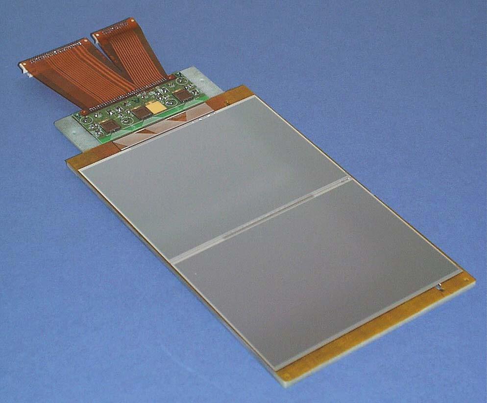
15 Strip (array) detectors Strip detectors are commonly used in particle physics and in event driven applications with high multiplicity. Characteristics Fully depleted sensor for good signal efficiency Low number of readout channels for a large active surface Fast readout speed If energy information is no critical the readout channel number can be reduced by capacitive and resistive charge division 1-dimensional position information orthogonal to strip direction. (2-dimensional position information can be achieved with double sided sensors) The strip electronics can contain complex electronics (discriminator, de-randomise buffer, counter e.t.c.) Typical strip pitch 25 m to 1mm, position resolution down to 1 m Used in high energy physics, autoradiography (betas), scanning devices in medicine (X-rays) e.t.c.
16 R Resistive charge division: Resistance will degrade noise performance, hence only applicable to large charge signals C Capacitive charge division: Small loss in S/N but only limited reduction of readout channels

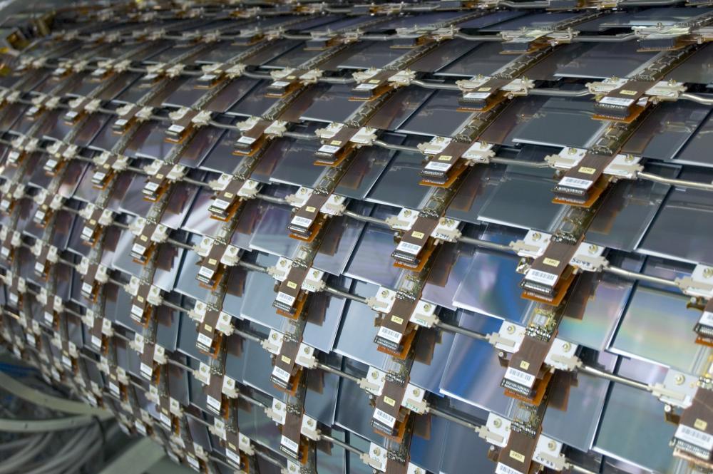
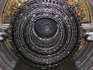
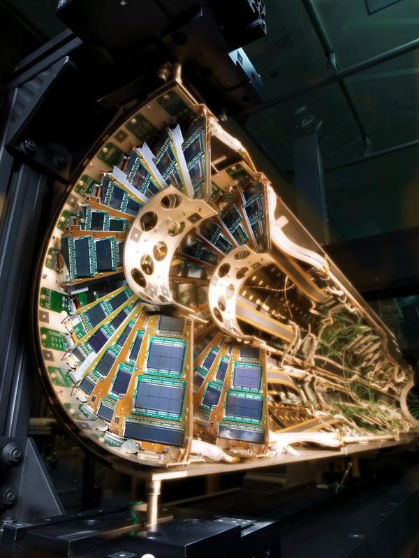
17 ATLAS SCT CMS TRACKER
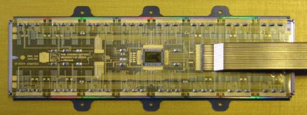
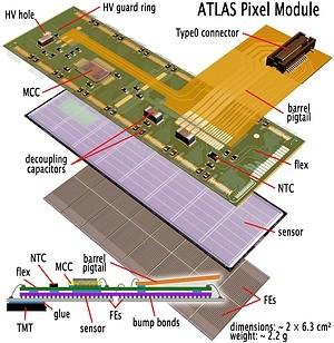
18 Pixel detectors A 2-dimensional sensor with readout electronics in every pixels. The sensor and the readout electronics are laid on top of each other flip-chip and connected by interconnecting bumps hybrid pixel detector. The monolithic pixel detectors is a recent development with readout electronics integrated into the pixel. Characteristics of pixel detectors: Fully depleted sensor for good signal efficiency Large number of readout channels Fast readout speed Can be used for imaging (integrating events) and for single event readout The pixel electronics can contain complex electronics (discriminator, de-randomise buffer, counter e.t.c.) Typical pixel pitch 25 m to 1mm, position resolution down to few m Used for medical(x-rays), space (X-rays), high energy physics e.t.c.
")

19 Charged track Sensor Bump (contact) Readout electronics Bumps before after reflow
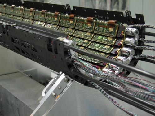
20 CMS ATLAS
21 Drift detectors Drift detectors give an alternative way of achieving 2-d readout to pixelised detectors. In the Drift detector the electric filed is horizontal (sidewards). A fully depleted drift detector has p+ strips implanted on both sides and a n+ strip/pad on one side. The p+ strips give the position information with the signal from drifting holes while the n+ strip collect electrons with fast time response and good energy resolution. Characteristics of a drift detector Fully depleted sensor for good signal efficiency Slow readout Good energy resolution Used in space (X.-rays), high multiplicity physics e.g. Heavy Ion and Nuclear Physics


22 ALICE silicon drift detector
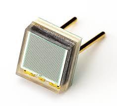
23 Photodiodes Semiconductors we have discussed have so far only provided the primary ionisation. In some applications (especially detecting low energy photons) the semiconductor sensor is turned into an amplifier by operating the sensor with very high fields causing charge multiplication Avalanche photodiodes. Avalanche photodiodes are widely used in optical data transmission where GaAs is the preferred material. Arrays of avalanche photodiodes are used in Silicon Photo Multipliers (used in calorimeters) Benefits: large signal from the sensor high speed compact (compared with other methods) work in magnetic field Penalty: linearity different amplification onset for electrons and holes. This effect is large for Si but small for GaAs.
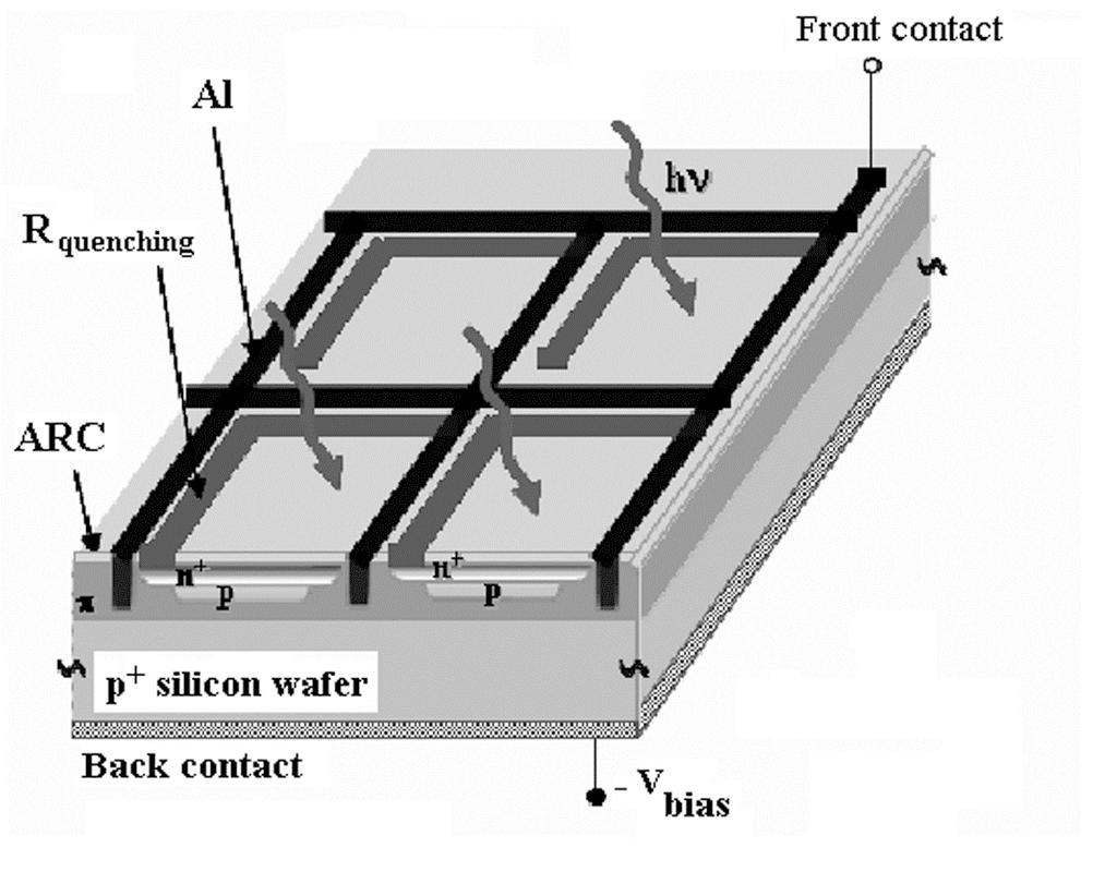
24 p+ (charge multiplication) n+ n n p undepleted bulk p+
 : ( S/N) - moderate gain (10-50) provided by thin highlydoped avalanche region (a few μm with high electrical field, ~a few 100")
25 LGAD (Low Gain Avalanche Diode) Low Gain Avalanche Diode pioneered by CNM. Now produced by HPK and FBK with similar performance (except breakdown values) BNL and Micro in near future. A lot of work also done within RD50 Gain (charge ratio of LGAD/diode) : ( S/N) - moderate gain (10-50) provided by thin highlydoped avalanche region (a few μm with high electrical field, ~a few 100 kv/cm) - depend on doping density - independent of sensor thickness Signal speed : ( trise) - Not very fast, rise time around ns - Rise time and duration depends on sensor thickness
26 Charge Couple Devices CCD's are widely used in video cameras. The sensors are not depleted structures but works with MOS depletion layers. For low noise and with low particle fluxes (like in astronomy) the CCD's must be cooled. In medicine CCD's are used together with converters like scintillators. The CCD's are pixelated by metal electrodes in one direction and by implants in the other direction. By changing the potential of the electrodes the charged collected by the CCD can be transported to the amplifier which is integrated with the CCD (monolithic). Characteristics of a CCD Non depleted (low efficiency for X-rays) Slow (since the charge has to be transported through many pixels) Pixels do not contain electronics hence no processing like setting threshold can be done in the pixel. Large number of pixels Typical pixel pitch 10 m, position resolution down to m Limited radiation tolerance Special processing that differs from industry road map.

27 Operation SLD pixel detector at SLAC
28 CMOS sensors Monolithic Analogue Pixel Sensors/CMOS sensors is a new emerging technology which is rapidly competing with CCDs in consumer products and HEP applications. Originally not depleted (low efficiency) new types developed for particle physics are now depleted Faster than CCD but still slow for innermost LHC regions Charge transport with diffusion (=> slow charge collection) Sufficient S/N at room temperature Uses CMOS processing technology and processes widely supported by industry Electronics in every pixel with common readout. Large number of pixels Typical pixel pitch 10 m, position resolution down to m Better radiation tolerance than CCDs, can now be used at LHC Technology preferred by Heavy Ion and Linear Collider communities. Can be made very thin => low X/X0


29 STAR CMOS pixel detector at RHIC and ALICE
 Each channel has an integrated")


30 DEPFET (DEpleted Field Effect Transistor structure) Each channel has an integrated FET to amplify the signal already in the detector which allow for building extremely thin sensors. MPI in Munich is building the vertex detector for Belle upgrade with this technology.
31 END LECTURE
32 Signal formation in the detector Delta pulse (photon) Continuous pulse (charged track)
Strip Detectors. Principal: Silicon strip detector. Ingrid--MariaGregor,SemiconductorsasParticleDetectors. metallization (Al) p +--strips
 p +--strips") Strip Detectors First detector devices using the lithographic capabilities of microelectronics First Silicon detectors -- > strip detectors Can be found in all high energy physics experiments of the last
Strip Detectors First detector devices using the lithographic capabilities of microelectronics First Silicon detectors -- > strip detectors Can be found in all high energy physics experiments of the last
Semiconductor Detector Systems
 Semiconductor Detector Systems Helmuth Spieler Physics Division, Lawrence Berkeley National Laboratory OXFORD UNIVERSITY PRESS ix CONTENTS 1 Detector systems overview 1 1.1 Sensor 2 1.2 Preamplifier 3
CMOS Detectors Ingeniously Simple!
 CMOS Detectors Ingeniously Simple! A.Schöning University Heidelberg B-Workshop Neckarzimmern 18.-20.2.2015 1 Detector System on Chip? 2 ATLAS Pixel Module 3 ATLAS Pixel Module MCC sensor FE-Chip FE-Chip
A High-Granularity Timing Detector for the Phase-II upgrade of the ATLAS Detector system
 A High-Granularity Timing Detector for the Phase-II upgrade of the ATLAS Detector system C.Agapopoulou on behalf of the ATLAS Lar -HGTD group 2017 IEEE Nuclear Science Symposium and Medical Imaging Conference
Silicon Detectors in High Energy Physics
 Thomas Bergauer (HEPHY Vienna) IPM Teheran 22 May 2011 Sunday: Schedule Semiconductor Basics (45 ) Silicon Detectors in Detector concepts: Pixels and Strips (45 ) Coffee Break Strip Detector Performance
Thin Silicon R&D for LC applications
 Thin Silicon R&D for LC applications D. Bortoletto Purdue University Status report Hybrid Pixel Detectors for LC Next Linear Collider:Physic requirements Vertexing 10 µ mgev σ r φ,z(ip ) 5µ m 3 / 2 p sin
A Prototype Amplifier-Discriminator Chip for the GLAST Silicon-Strip Tracker
 A Prototype Amplifier-Discriminator Chip for the GLAST Silicon-Strip Tracker Robert P. Johnson Pavel Poplevin Hartmut Sadrozinski Ned Spencer Santa Cruz Institute for Particle Physics The GLAST Project
Understanding the Properties of Gallium Implanted LGAD Timing Detectors
 Understanding the Properties of Gallium Implanted LGAD Timing Detectors Arifin Luthfi Maulana 1 and Stefan Guindon 2 1 Institut Teknologi Bandung, Bandung, Indonesia 2 CERN, Geneva, Switzerland Corresponding
UFSD: Ultra-Fast Silicon Detector
 UFSD: Ultra-Fast Silicon Detector Basic goals of UFSD (aka Low-Gain Avalanche Diode) A parameterization of time resolution State of the art How to do better Overview of the sensor design Example of application
Figure Responsivity (A/W) Figure E E-09.
 Figure E E-09.") OSI Optoelectronics, is a leading manufacturer of fiber optic components for communication systems. The products offer range for Silicon, GaAs and InGaAs to full turnkey solutions. Photodiodes are semiconductor
OSI Optoelectronics, is a leading manufacturer of fiber optic components for communication systems. The products offer range for Silicon, GaAs and InGaAs to full turnkey solutions. Photodiodes are semiconductor
Detector Electronics
 DoE Basic Energy Sciences (BES) Neutron & Photon Detector Workshop August 1-3, 2012 Gaithersburg, Maryland Detector Electronics spieler@lbl.gov Detector System Tutorials at http://www-physics.lbl.gov/~spieler
Simulation of High Resistivity (CMOS) Pixels
 Pixels") Simulation of High Resistivity (CMOS) Pixels Stefan Lauxtermann, Kadri Vural Sensor Creations Inc. AIDA-2020 CMOS Simulation Workshop May 13 th 2016 OUTLINE 1. Definition of High Resistivity Pixel Also
Simulation of High Resistivity (CMOS) Pixels Stefan Lauxtermann, Kadri Vural Sensor Creations Inc. AIDA-2020 CMOS Simulation Workshop May 13 th 2016 OUTLINE 1. Definition of High Resistivity Pixel Also
Figure Figure E E-09. Dark Current (A) 1.
 1.") OSI Optoelectronics, is a leading manufacturer of fiber optic components for communication systems. The products offer range for Silicon, GaAs and InGaAs to full turnkey solutions. Photodiodes are semiconductor
OSI Optoelectronics, is a leading manufacturer of fiber optic components for communication systems. The products offer range for Silicon, GaAs and InGaAs to full turnkey solutions. Photodiodes are semiconductor
SRM INSTITUTE OF SCIENCE AND TECHNOLOGY (DEEMED UNIVERSITY)
") SRM INSTITUTE OF SCIENCE AND TECHNOLOGY (DEEMED UNIVERSITY) QUESTION BANK I YEAR B.Tech (II Semester) ELECTRONIC DEVICES (COMMON FOR EC102, EE104, IC108, BM106) UNIT-I PART-A 1. What are intrinsic and
SRM INSTITUTE OF SCIENCE AND TECHNOLOGY (DEEMED UNIVERSITY) QUESTION BANK I YEAR B.Tech (II Semester) ELECTRONIC DEVICES (COMMON FOR EC102, EE104, IC108, BM106) UNIT-I PART-A 1. What are intrinsic and
PoS(EPS-HEP 2009)150. Silicon Detectors for the slhc - an Overview of Recent RD50 Results. Giulio Pellegrini 1. On behalf of CERN RD50 collaboration
150. Silicon Detectors for the slhc - an Overview of Recent RD50 Results. Giulio Pellegrini 1. On behalf of CERN RD50 collaboration") Silicon Detectors for the slhc - an Overview of Recent RD50 Results 1 Centro Nacional de Microelectronica CNM- IMB-CSIC, Barcelona Spain E-mail: giulio.pellegrini@imb-cnm.csic.es On behalf of CERN RD50
Silicon Detectors for the slhc - an Overview of Recent RD50 Results 1 Centro Nacional de Microelectronica CNM- IMB-CSIC, Barcelona Spain E-mail: giulio.pellegrini@imb-cnm.csic.es On behalf of CERN RD50
MAPS-based ECAL Option for ILC
 MAPS-based ECAL Option for ILC, Spain Konstantin Stefanov On behalf of J. Crooks, P. Dauncey, A.-M. Magnan, Y. Mikami, R. Turchetta, M. Tyndel, G. Villani, N. Watson, J. Wilson v Introduction v ECAL with
Recent Development and Study of Silicon Solid State Photomultiplier (MRS Avalanche Photodetector)
") Recent Development and Study of Silicon Solid State Photomultiplier (MRS Avalanche Photodetector) Valeri Saveliev University of Obninsk, Russia Vienna Conference on Instrumentation Vienna, 20 February
Recent Development and Study of Silicon Solid State Photomultiplier (MRS Avalanche Photodetector) Valeri Saveliev University of Obninsk, Russia Vienna Conference on Instrumentation Vienna, 20 February
A High-Granularity Timing Detector for the Phase-II upgrade of the ATLAS Calorimeter system Detector concept description and first beam test results
 A High-Granularity Timing Detector for the Phase-II upgrade of the ATLAS Calorimeter system Detector concept description and first beam test results 03/10/2017 ATL-LARG-SLIDE-2017-858 Didier Lacour On
Silicon sensors for radiant signals. D.Sc. Mikko A. Juntunen
 Silicon sensors for radiant signals D.Sc. Mikko A. Juntunen 2017 01 16 Today s outline Introduction Basic physical principles PN junction revisited Applications Light Ionizing radiation X-Ray sensors in
Development of Pixel Detectors for the Inner Tracker Upgrade of the ATLAS Experiment
 Development of Pixel Detectors for the Inner Tracker Upgrade of the ATLAS Experiment Natascha Savić L. Bergbreiter, J. Breuer, A. Macchiolo, R. Nisius, S. Terzo IMPRS, Munich # 29.5.215 Franz Dinkelacker
Engineering Medical Optics BME136/251 Winter 2018
 Engineering Medical Optics BME136/251 Winter 2018 Monday/Wednesday 2:00-3:20 p.m. Beckman Laser Institute Library, MSTB 214 (lab) *1/17 UPDATE Wednesday, 1/17 Optics and Photonic Devices III: homework
The Medipix3 Prototype, a Pixel Readout Chip Working in Single Photon Counting Mode with Improved Spectrometric Performance
 26 IEEE Nuclear Science Symposium Conference Record NM1-6 The Medipix3 Prototype, a Pixel Readout Chip Working in Single Photon Counting Mode with Improved Spectrometric Performance R. Ballabriga, M. Campbell,
Digital Integrated Circuits A Design Perspective. The Devices. Digital Integrated Circuits 2nd Devices
 Digital Integrated Circuits A Design Perspective The Devices The Diode The diodes are rarely explicitly used in modern integrated circuits However, a MOS transistor contains at least two reverse biased
Chromatic X-Ray imaging with a fine pitch CdTe sensor coupled to a large area photon counting pixel ASIC
 Chromatic X-Ray imaging with a fine pitch CdTe sensor coupled to a large area photon counting pixel ASIC R. Bellazzini a,b, G. Spandre a*, A. Brez a, M. Minuti a, M. Pinchera a and P. Mozzo b a INFN Pisa
Preparing for the Future: Upgrades of the CMS Pixel Detector
 : KSETA Plenary Workshop, Durbach, KIT Die Forschungsuniversität in der Helmholtz-Gemeinschaft www.kit.edu Large Hadron Collider at CERN Since 2015: proton proton collisions @ 13 TeV Four experiments:
Muon detection in security applications and monolithic active pixel sensors
 Muon detection in security applications and monolithic active pixel sensors Tracking in particle physics Gaseous detectors Silicon strips Silicon pixels Monolithic active pixel sensors Cosmic Muon tomography
Optical Receivers Theory and Operation
 Optical Receivers Theory and Operation Photo Detectors Optical receivers convert optical signal (light) to electrical signal (current/voltage) Hence referred O/E Converter Photodetector is the fundamental
Photodiode: LECTURE-5
 LECTURE-5 Photodiode: Photodiode consists of an intrinsic semiconductor sandwiched between two heavily doped p-type and n-type semiconductors as shown in Fig. 3.2.2. Sufficient reverse voltage is applied
Lecture 18: Photodetectors
 Lecture 18: Photodetectors Contents 1 Introduction 1 2 Photodetector principle 2 3 Photoconductor 4 4 Photodiodes 6 4.1 Heterojunction photodiode.................... 8 4.2 Metal-semiconductor photodiode................
 http://clicdp.cern.ch Hybrid Pixel Detectors with Active-Edge Sensors for the CLIC Vertex Detector Simon Spannagel on behalf of the CLICdp Collaboration Experimental Conditions at CLIC CLIC beam structure
Simulation and test of 3D silicon radiation detectors
 Simulation and test of 3D silicon radiation detectors C.Fleta 1, D. Pennicard 1, R. Bates 1, C. Parkes 1, G. Pellegrini 2, M. Lozano 2, V. Wright 3, M. Boscardin 4, G.-F. Dalla Betta 4, C. Piemonte 4,
Key Questions ECE 340 Lecture 28 : Photodiodes
 Things you should know when you leave Key Questions ECE 340 Lecture 28 : Photodiodes Class Outline: How do the I-V characteristics change with illumination? How do solar cells operate? How do photodiodes
Seminar. BELLE II Particle Identification Detector and readout system. Andrej Seljak advisor: Prof. Samo Korpar October 2010
 Seminar BELLE II Particle Identification Detector and readout system Andrej Seljak advisor: Prof. Samo Korpar October 2010 Outline Motivation BELLE experiment and future upgrade plans RICH proximity focusing
Design and Performance of a Pinned Photodiode CMOS Image Sensor Using Reverse Substrate Bias
 Design and Performance of a Pinned Photodiode CMOS Image Sensor Using Reverse Substrate Bias 13 September 2017 Konstantin Stefanov Contents Background Goals and objectives Overview of the work carried
UFSD: Ultra-Fast Silicon Detector
 UFSD: Ultra-Fast Silicon Detector Basic goals of UFSD A parameterization of time resolution State of the art How to do better Overview of the sensor design First Results Nicolo Cartiglia with M. Baselga,
High Luminosity ATLAS vs. CMOS Sensors
 High Luminosity ATLAS vs. CMOS Sensors Where we currently are and where we d like to be Jens Dopke, STFC RAL 1 Disclaimer I usually do talks on things where I generated all the imagery myself (ATLAS Pixels/IBL)
Integrated CMOS sensor technologies for the CLIC tracker
 CLICdp-Conf-2017-011 27 June 2017 Integrated CMOS sensor technologies for the CLIC tracker M. Munker 1) On behalf of the CLICdp collaboration CERN, Switzerland, University of Bonn, Germany Abstract Integrated
TPC Readout with GEMs & Pixels
 TPC Readout with GEMs & Pixels + Linear Collider Tracking Directional Dark Matter Detection Directional Neutron Spectroscopy? Sven Vahsen Lawrence Berkeley Lab Cygnus 2009, Cambridge Massachusetts 2 Our
Low Power Sensor Concepts
 Low Power Sensor Concepts Konstantin Stefanov 11 February 2015 Introduction The Silicon Pixel Tracker (SPT): The main driver is low detector mass Low mass is enabled by low detector power Benefits the
Prepared by: Dr. Rishi Prakash, Dept of Electronics and Communication Engineering Page 1 of 5
 Microwave tunnel diode Some anomalous phenomena were observed in diode which do not follows the classical diode equation. This anomalous phenomena was explained by quantum tunnelling theory. The tunnelling
Fundamentals of CMOS Image Sensors
 CHAPTER 2 Fundamentals of CMOS Image Sensors Mixed-Signal IC Design for Image Sensor 2-1 Outline Photoelectric Effect Photodetectors CMOS Image Sensor(CIS) Array Architecture CIS Peripherals Design Considerations
UNIT IX ELECTRONIC DEVICES
 UNT X ELECTRONC DECES Weightage Marks : 07 Semiconductors Semiconductors diode-- characteristics in forward and reverse bias, diode as rectifier. - characteristics of LED, Photodiodes, solarcell and Zener
the need for an intensifier
 * The LLLCCD : Low Light Imaging without the need for an intensifier Paul Jerram, Peter Pool, Ray Bell, David Burt, Steve Bowring, Simon Spencer, Mike Hazelwood, Ian Moody, Neil Catlett, Philip Heyes Marconi
ECE520 VLSI Design. Lecture 2: Basic MOS Physics. Payman Zarkesh-Ha
 ECE520 VLSI Design Lecture 2: Basic MOS Physics Payman Zarkesh-Ha Office: ECE Bldg. 230B Office hours: Wednesday 2:00-3:00PM or by appointment E-mail: pzarkesh@unm.edu Slide: 1 Review of Last Lecture Semiconductor
INTRODUCTION TO MOS TECHNOLOGY
 INTRODUCTION TO MOS TECHNOLOGY 1. The MOS transistor The most basic element in the design of a large scale integrated circuit is the transistor. For the processes we will discuss, the type of transistor
VII. IR Arrays & Readout VIII.CCDs & Readout. This lecture course follows the textbook Detection of
 Detection of Light VII. IR Arrays & Readout VIII.CCDs & Readout This lecture course follows the textbook Detection of Light 4-3-2016 by George Rieke, Detection Cambridge of Light Bernhard Brandl University
Week 9: Chap.13 Other Semiconductor Material
 Week 9: Chap.13 Other Semiconductor Material Exam Other Semiconductors and Geometries -- Why --- CZT properties -- Silicon Structures --- CCD s Gamma ray Backgrounds The MIT Semiconductor Subway (of links
Optimization of amplifiers for Monolithic Active Pixel Sensors
 Optimization of amplifiers for Monolithic Active Pixel Sensors A. Dorokhov a, on behalf of the CMOS & ILC group of IPHC a Institut Pluridisciplinaire Hubert Curien, Département Recherches Subatomiques,
Section:A Very short answer question
 Section:A Very short answer question 1.What is the order of energy gap in a conductor, semi conductor, and insulator?. Conductor - no energy gap Semi Conductor - It is of the order of 1 ev. Insulator -
Detectors for microscopy - CCDs, APDs and PMTs. Antonia Göhler. Nov 2014
 Detectors for microscopy - CCDs, APDs and PMTs Antonia Göhler Nov 2014 Detectors/Sensors in general are devices that detect events or changes in quantities (intensities) and provide a corresponding output,
The HGTD: A SOI Power Diode for Timing Detection Applications
 The HGTD: A SOI Power Diode for Timing Detection Applications Work done in the framework of RD50 Collaboration (CERN) M. Carulla, D. Flores, S. Hidalgo, D. Quirion, G. Pellegrini IMB-CNM (CSIC), Spain
A flexible compact readout circuit for SPAD arrays ABSTRACT Keywords: 1. INTRODUCTION 2. THE SPAD 2.1 Operation 7780C - 55
 A flexible compact readout circuit for SPAD arrays Danial Chitnis * and Steve Collins Department of Engineering Science University of Oxford Oxford England OX13PJ ABSTRACT A compact readout circuit that
Recent Technological Developments on LGAD and ilgad Detectors for Tracking and Timing Applications
 Recent Technological Developments on LGAD and ilgad Detectors for Tracking and Timing Applications G. Pellegrini 1, M. Baselga 1, M. Carulla 1, V. Fadeyev 2, P. Fernández-Martínez 1, M. Fernández García
Development of n-in-p Active Edge Pixel Detectors for ATLAS ITK Upgrade
 Development of n-in-p Active Edge Pixel Detectors for ATLAS ITK Upgrade Tasneem Rashid Supervised by: Abdenour Lounis. PHENIICS Fest 2017 30th OUTLINE Introduction: - The Large Hadron Collider (LHC). -
Production of HPDs for the LHCb RICH Detectors
 Production of HPDs for the LHCb RICH Detectors LHCb RICH Detectors Hybrid Photon Detector Production Photo Detector Test Facilities Test Results Conclusions IEEE Nuclear Science Symposium Wyndham, 24 th
ITk silicon strips detector test beam at DESY
 ITk silicon strips detector test beam at DESY Lucrezia Stella Bruni Nikhef Nikhef ATLAS outing 29/05/2015 L. S. Bruni - Nikhef 1 / 11 Qualification task I Participation at the ITk silicon strip test beams
XRF Instrumentation. Introduction to spectrometer
 XRF Instrumentation Introduction to spectrometer AMPTEK, INC., Bedford, MA 01730 Ph: +1 781 275 2242 Fax: +1 781 275 3470 sales@amptek.com 1 Instrument Excitation source Sample X-ray tube or radioisotope
Noise Performance Analysis for the Silicon Tracking System Detector and Front-End Electronics
 Noise Performance Analysis for the Silicon Tracking System Detector and Front-End Electronics Weronika Zubrzycka, Krzysztof Kasiński zubrzycka@agh.edu.pl, kasinski@agh.edu.pl Department of Measurement
Readout Electronics. P. Fischer, Heidelberg University. Silicon Detectors - Readout Electronics P. Fischer, ziti, Uni Heidelberg, page 1
 Readout Electronics P. Fischer, Heidelberg University Silicon Detectors - Readout Electronics P. Fischer, ziti, Uni Heidelberg, page 1 We will treat the following questions: 1. How is the sensor modeled?
STATE-OF-THE-ART SILICON DETECTORS FOR X-RAY SPECTROSCOPY
 Copyright JCPDS - International Centre for Diffraction Data 2004, Advances in X-ray Analysis, Volume 47. 47 STATE-OF-THE-ART SILICON DETECTORS FOR X-RAY SPECTROSCOPY P. Lechner* 1, R. Hartmann* 1, P. Holl*
MOSFET short channel effects
 MOSFET short channel effects overview Five different short channel effects can be distinguished: velocity saturation drain induced barrier lowering (DIBL) impact ionization surface scattering hot electrons
A timing layer for charge particles in CMS
 A timing layer for charge particles in CMS Is it possible to build a tracker with concurrent excellent time and position resolution? Barrel Can we provide in one, or in combination Endcap Timing resolution
UNIT VIII-SPECIAL PURPOSE ELECTRONIC DEVICES. 1. Explain tunnel Diode operation with the help of energy band diagrams.
 UNIT III-SPECIAL PURPOSE ELECTRONIC DEICES 1. Explain tunnel Diode operation with the help of energy band diagrams. TUNNEL DIODE: A tunnel diode or Esaki diode is a type of semiconductor diode which is
The High-Voltage Monolithic Active Pixel Sensor for the Mu3e Experiment
 The High-Voltage Monolithic Active Pixel Sensor for the Mu3e Experiment Shruti Shrestha On Behalf of the Mu3e Collaboration International Conference on Technology and Instrumentation in Particle Physics
Introduction. Chapter 1
 1 Chapter 1 Introduction During the last decade, imaging with semiconductor devices has been continuously replacing conventional photography in many areas. Among all the image sensors, the charge-coupled-device
Characterisation of Hybrid Pixel Detectors with capacitive charge division
 Characterisation of Hybrid Pixel Detectors with capacitive charge division M. Caccia 1, S.Borghi, R. Campagnolo,M. Battaglia, W. Kucewicz, H.Palka, A. Zalewska, K.Domanski, J.Marczewski, D.Tomaszewski
Fast CMOS Transimpedance Amplifier and Comparator circuit for readout of silicon strip detectors at LHC experiments
 Fast CMOS Transimpedance Amplifier and Comparator circuit for readout of silicon strip detectors at LHC experiments Jan Kaplon - CERN Wladek Dabrowski - FPN/UMM Cracow Pepe Bernabeu IFIC Valencia Carlos
Lecture 8 Optical Sensing. ECE 5900/6900 Fundamentals of Sensor Design
 ECE 5900/6900: Fundamentals of Sensor Design Lecture 8 Optical Sensing 1 Optical Sensing Q: What are we measuring? A: Electromagnetic radiation labeled as Ultraviolet (UV), visible, or near,mid-, far-infrared
Evaluation of the Radiation Tolerance of Several Generations of SiGe Heterojunction Bipolar Transistors Under Radiation Exposure
 1 Evaluation of the Radiation Tolerance of Several Generations of SiGe Heterojunction Bipolar Transistors Under Radiation Exposure J. Metcalfe, D. E. Dorfan, A. A. Grillo, A. Jones, F. Martinez-McKinney,
Objective Type Questions 1. Why pure semiconductors are insulators at 0 o K? 2. What is effect of temperature on barrier voltage? 3.
 Objective Type Questions 1. Why pure semiconductors are insulators at 0 o K? 2. What is effect of temperature on barrier voltage? 3. What is difference between electron and hole? 4. Why electrons have
Front-End and Readout Electronics for Silicon Trackers at the ILC
 2005 International Linear Collider Workshop - Stanford, U.S.A. Front-End and Readout Electronics for Silicon Trackers at the ILC M. Dhellot, J-F. Genat, H. Lebbolo, T-H. Pham, and A. Savoy Navarro LPNHE
An introduction to Depletion-mode MOSFETs By Linden Harrison
 An introduction to Depletion-mode MOSFETs By Linden Harrison Since the mid-nineteen seventies the enhancement-mode MOSFET has been the subject of almost continuous global research, development, and refinement
Why p-type is better than n-type? or Electric field in heavily irradiated silicon detectors
 Why p-type is better than n-type? or Electric field in heavily irradiated silicon detectors G.Kramberger, V. Cindro, I. Mandić, M. Mikuž, M. Milovanović, M. Zavrtanik Jožef Stefan Institute Ljubljana,
Semiconductor Devices Lecture 5, pn-junction Diode
 Semiconductor Devices Lecture 5, pn-junction Diode Content Contact potential Space charge region, Electric Field, depletion depth Current-Voltage characteristic Depletion layer capacitance Diffusion capacitance
Application of avalanche photodiodes as a readout for scintillator tile-fiber systems
 Application of avalanche photodiodes as a readout for scintillator tile-fiber systems C. Cheshkov a, G. Georgiev b, E. Gouchtchine c,l.litov a, I. Mandjoukov a, V. Spassov d a Faculty of Physics, Sofia
Photons and solid state detection
 Photons and solid state detection Photons represent discrete packets ( quanta ) of optical energy Energy is hc/! (h: Planck s constant, c: speed of light,! : wavelength) For solid state detection, photons
Tutors Dominik Dannheim, Thibault Frisson (CERN, Geneva, Switzerland)
") Danube School on Instrumentation in Elementary Particle & Nuclear Physics University of Novi Sad, Serbia, September 8 th 13 th, 2014 Lab Experiment: Characterization of Silicon Photomultipliers Dominik
Danube School on Instrumentation in Elementary Particle & Nuclear Physics University of Novi Sad, Serbia, September 8 th 13 th, 2014 Lab Experiment: Characterization of Silicon Photomultipliers Dominik
ATLAS strip detector upgrade for the HL-LHC
 ATL-INDET-PROC-2015-010 26 August 2015, On behalf of the ATLAS collaboration Santa Cruz Institute for Particle Physics, University of California, Santa Cruz E-mail: zhijun.liang@cern.ch Beginning in 2024,
SILICON DRIFT DETECTORS (SDDs) [1] with integrated. Preliminary Results on Compton Electrons in Silicon Drift Detector
![SILICON DRIFT DETECTORS (SDDs) [1] with integrated. Preliminary Results on Compton Electrons in Silicon Drift Detector](/thumbs/71/65601707.jpg "SILICON DRIFT DETECTORS (SDDs) [1] with integrated. Preliminary Results on Compton Electrons in Silicon Drift Detector") Preliminary Results on Compton Electrons in Silicon Drift Detector T. Çonka-Nurdan, K. Nurdan, K. Laihem, A. H. Walenta, C. Fiorini, B. Freisleben, N. Hörnel, N. A. Pavel, and L. Strüder Abstract Silicon
Preliminary Results on Compton Electrons in Silicon Drift Detector T. Çonka-Nurdan, K. Nurdan, K. Laihem, A. H. Walenta, C. Fiorini, B. Freisleben, N. Hörnel, N. A. Pavel, and L. Strüder Abstract Silicon
Calorimetry in particle physics experiments
 Calorimetry in particle physics experiments Unit n. 7 Front End and Trigger electronics Roberta Arcidiacono Lecture overview Signal processing Some info on calorimeter FE Pre-amplifiers Charge sensitive
Characterization Of Pin Diode Silicon Radiation Detector
 Journal on Intelligent Electronic Systems, Vol.1, No.1, November 007 Characterization Of Pin Diode Silicon Radiation Detector 47 Abstract 1 3 Samichi Srivastava, Rabinber Henry, Anita Topka R 1 PG Scholar,
Università degli Studi di Roma Tor Vergata Dipartimento di Ingegneria Elettronica. Analogue Electronics. Paolo Colantonio A.A.
 Università degli Studi di Roma Tor Vergata Dipartimento di Ingegneria Elettronica Analogue Electronics Paolo Colantonio A.A. 2015-16 Introduction: materials Conductors e.g. copper or aluminum have a cloud
Silicon Sensor Developments for the CMS Tracker Upgrade
 Silicon Sensor Developments for the CMS Tracker Upgrade on behalf of the CMS tracker collaboration University of Hamburg, Germany E-mail: Joachim.Erfle@desy.de CMS started a campaign to identify the future
Monolithic Pixel Sensors in SOI technology R&D activities at LBNL
 Monolithic Pixel Sensors in SOI technology R&D activities at LBNL Lawrence Berkeley National Laboratory M. Battaglia, L. Glesener (UC Berkeley & LBNL), D. Bisello, P. Giubilato (LBNL & INFN Padova), P.
Detectors for Optical Communications
 Optical Communications: Circuits, Systems and Devices Chapter 3: Optical Devices for Optical Communications lecturer: Dr. Ali Fotowat Ahmady Sep 2012 Sharif University of Technology 1 Photo All detectors
AVALANCHE PHOTODIODES FOR THE CMS ELECTROMAGNETIC CALORIMETER
 AVALANCHE PHOTODIODES FOR THE CMS ELECTROMAGNETIC CALORIMETER B. Patel, R. Rusack, P. Vikas(email:Pratibha.Vikas@cern.ch) University of Minnesota, Minneapolis, U.S.A. Y. Musienko, S. Nicol, S.Reucroft,
How Does One Obtain Spectral/Imaging Information! "
 How Does One Obtain Spectral/Imaging Information! How do we measure the position, energy, and arrival time of! an X-ray photon?! " What we observe depends on the instruments that one observes with!" In
X-ray Detectors at DESY
 X-ray Detectors at DESY (Contribution given at the FEL2006 meeting in Berlin) DESY The European XFEL Time structure: difference with others Electron bunch trains; up to 3000 bunches in 600 μsec, repeated
Silicon detectors for particle physics laboratory
 Silicon detectors for particle physics laboratory R. Bates 1, L. Eklund, N. Pacifico and M. Milovanovic 3 This laboratory would not have been possible without the financial help from the particle physics
FIBER OPTICS. Prof. R.K. Shevgaonkar. Department of Electrical Engineering. Indian Institute of Technology, Bombay. Lecture: 20
 FIBER OPTICS Prof. R.K. Shevgaonkar Department of Electrical Engineering Indian Institute of Technology, Bombay Lecture: 20 Photo-Detectors and Detector Noise Fiber Optics, Prof. R.K. Shevgaonkar, Dept.
Bipolar Junction Transistors
 Bipolar Junction Transistors Invented in 1948 at Bell Telephone laboratories Bipolar junction transistor (BJT) - one of the major three terminal devices Three terminal devices more useful than two terminal
NAME: Last First Signature
 UNIVERSITY OF CALIFORNIA, BERKELEY College of Engineering Department of Electrical Engineering and Computer Sciences EE 130: IC Devices Spring 2003 FINAL EXAMINATION NAME: Last First Signature STUDENT
CONTENTS. 2.2 Schrodinger's Wave Equation 31. PART I Semiconductor Material Properties. 2.3 Applications of Schrodinger's Wave Equation 34
 CONTENTS Preface x Prologue Semiconductors and the Integrated Circuit xvii PART I Semiconductor Material Properties CHAPTER 1 The Crystal Structure of Solids 1 1.0 Preview 1 1.1 Semiconductor Materials
Single Photon Counting in the Visible
 Single Photon Counting in the Visible OUTLINE System Definition DePMOS and RNDR Device Concept RNDR working principle Experimental results Gatable APS devices Achieved and achievable performance Conclusions
Reg. No. : Question Paper Code : B.E./B.Tech. DEGREE EXAMINATION, NOVEMBER/DECEMBER Second Semester
 WK 5 Reg. No. : Question Paper Code : 27184 B.E./B.Tech. DEGREE EXAMINATION, NOVEMBER/DECEMBER 2015. Time : Three hours Second Semester Electronics and Communication Engineering EC 6201 ELECTRONIC DEVICES
Introduction to X-ray Detectors for Synchrotron Radiation Applications
 Introduction to X-ray Detectors for Synchrotron Radiation Applications Pablo Fajardo Instrumentation Services and Development Division ESRF, Grenoble EIROforum School on Instrumentation (ESI 2011) Outline
Lecture 2 p-n junction Diode characteristics. By Asst. Prof Dr. Jassim K. Hmood
 Electronic I Lecture 2 p-n junction Diode characteristics By Asst. Prof Dr. Jassim K. Hmood THE p-n JUNCTION DIODE The pn junction diode is formed by fabrication of a p-type semiconductor region in intimate
Optical Fiber Communication Lecture 11 Detectors
 Optical Fiber Communication Lecture 11 Detectors Warriors of the Net Detector Technologies MSM (Metal Semiconductor Metal) PIN Layer Structure Semiinsulating GaAs Contact InGaAsP p 5x10 18 Absorption InGaAs
AIDA-2020 Advanced European Infrastructures for Detectors at Accelerators. Milestone Report
 AIDA-2020-MS15 AIDA-2020 Advanced European Infrastructures for Detectors at Accelerators Milestone Report Design specifications of test stations for irradiated silicon sensors and LHC oriented front-end
Design and Test of a 65nm CMOS Front-End with Zero Dead Time for Next Generation Pixel Detectors
 Design and Test of a 65nm CMOS Front-End with Zero Dead Time for Next Generation Pixel Detectors L. Gaioni a,c, D. Braga d, D. Christian d, G. Deptuch d, F. Fahim d,b. Nodari e, L. Ratti b,c, V. Re a,c,